1. Introduction
The trend toward implementing non-volatile memory (NVM) as the main memory in portable computer systems incurs a security issue. It is commonly accepted that the non-volatility of the NVM (e.g., STT-MRAM, PRAM) improves the overall performance of a system, for instance, by accelerating the booting process and by reducing file transactions in the database system [
1,
2,
3]. However, NVM is more vulnerable than volatile DRAM since NVM sustains data even after the system shutdown. This problem encounters a physical attack: once a device is physically obtained, the attacker can easily extract the stored data in the NVM by installing the memory module in a specialized attacking system and executing a memory dump, even though the stolen device is protected by a password [
4].
One simple solution to protect against the physical attack is to encrypt all data in the memory with a symmetric key algorithm, which is referred to as a bulk encryption or a whole encryption in the literature [
5]; bulk encryption encrypts all data in memory when power is suspended, and whole encryption encrypts data for each memory write operation. Unfortunately, the randomizing property of standard encryption causes avalanche effect, which increases the number of flipped bits affecting energy consumption and lifetime of the memory [
6,
7,
8]. Reduction of the flip penalty is a crucial problem, since the bit flip increases energy consumption and degrades the durability of memory cells in NVM. Many works have been introduced to reduce the flip penalty in an NVM structure [
9,
10,
11,
12], since it is known that the bit write overhead in NVM is 2–3 times more than that of DRAM [
13,
14].
Stream cipher is an XOR-based encryption scheme, which generates ciphertext by XORing a random keystream to the plaintext. The one-time pad (OTP) encryption is a simple and representative example, where the message is encrypted by XORing the one-time keystream. Another typical example is the counter (CTR) mode in AES block cipher: the ciphertext is an XOR of the plaintext and the random keystream generated from the AES function. If we consider reusing the keystream in a stream cipher, it may provide a solution to minimize the flip penalty in a ciphertext; an XOR operation preserves the bit flip of unchanged messages between a plaintext and a ciphertext. However, reusing the keystream is not semantically secure, since given two ciphertexts the partial knowledge of plaintexts is revealed (assume that and , then we get , where k is the keystream). On the other hand, if a fresh keystream is applied for each write operation, it causes the same flip penalty problem again since each ciphertext is an independent random string. In a sense, there is an incompatible trade-off between security and performance.
When considering physical attacks, it is possible to control this trade-off by employing a periodic updating approach. In physical attacks, obtaining a snapshot of the memory takes a certain amount of time: the attacker requires a process of extracting the memory chip, making a snapshot in a different device, and restoring the chip back to the device. In this case, it is safe to reuse the keystream if we refresh it before the attacker obtains another snapshot. As long as the keystream is updated before the next snapshot, it operates exactly the same as an OTP encryption from the attacker’s view. In this context, the security level of the scheme is now controlled by a refresh period of the keystream: short (frequent) refresh period enhances the security, while long refresh period reuses more keystream and enhances the performance.
While maintaining a reliable refresh period, it would be ideal to apply the stream cipher to the whole memory. However, the keystream generation in stream cipher requires a nonce stored in an additional memory space, where the nonce is required for each block independently. To apply stream cipher for the entire memory blocks, the nonce must be stored separately as many as the number of blocks; assuming 16 GB memory with a 64B block and the nonce value as an integer (4B), we require 262,144 separate nonce values which involves 1 GB additional storage. Not to mention the storage overhead, large storage requirement forces the nonce to be stored in the off-chip memory (i.e., external to the processor). If the nonce is exposed to the external memory, the adversary might manipulate the nonce values to gain useful information.
Fortunately, we can tackle this nonce storage problem by focusing on the active (write-intensive) data. In most cases, the data used in applications represents temporal locality; there are only a few blocks that actually affect the memory-write performance. If we classify active blocks just enough to store their nonce in the processor, we can apply a stream cipher to the write-sensitive data to mitigate the flip penalty while maintaining their nonce in the on-chip processor. For instance, if we assume the nonce value as an integer (4B), we can utilize 1024 lines of active blocks for 4 KB nonce storage, which is sufficient to be stored in the on-chip memory. We can update the active blocks dynamically by keeping track of the access pattern, or relying on the static profiling of the application.
In this paper, we propose a Secure Hybrid Encryption with Less Flip (shelf) for Non-volatile Memory (NVM), or NVM-shelf, to control the trade-off between security and flip penalty by managing the keystream refresh period. The NVM-shelf is a hybrid encryption: we categorize active/inert blocks by managing a reference flag table which stores the access history of data blocks on current use, and apply a stream cipher to the active blocks with reusing the keystream in a certain period of time. As a stream cipher, we propose a modified version of the counter (CTR) mode in the AES block cipher where the nonce values of the active blocks are stored in a small table, which is named as timestamp-table. When we map a physical address of each block into the counter of the CTR mode, blocks with different addresses in the same period are encrypted using a keystream different from one another. Each block with the same address is encrypted using a distinct keystream for a separate period. For the inert blocks, any encryption scheme can be adopted; we simply utilize the electronic codebook (ECB) mode in the AES block cipher using a key and a block address without any nonce so that no additional memory space is required for the inert blocks.
The original CTR mode engages AES as a pseudorandom function (PRF), and it takes three inputs: counter (or nonce), key, and IV. We modify the input to use a block address, a global key, and a nonce where the nonce changes every period. The block address is an address tag of the cache block which lets the PRF generate a different output for each cache block. The global key is an internal secret key that is secured in a processor area, which ensures that the attacker cannot guess the PRF output by utilizing some known information in the memory. We compute the nonce by dividing the timestamp by update period. The timestamp is a real-time cycle at the moment the memory-write occurs, and the update period is a configurable constant which defines the interval of keystream reuse. If the update period is smaller enough than the time it takes to perform a physical attack (memory extraction and making snapshots), active blocks in the CTR mode are semantically secure against a physical adversary.
We performed an experiment based on the timed-QEMU simulator (TQSIM) [
15], by modifying the cache hardware to support the NVM-shelf algorithm. According to our experiment, the proposed NVM-shelf shows only 3% flip penalty while the whole encryption (which encrypts all data with the ECB mode) shows a flip penalty of 135%. Our NVM-shelf improves the energy consumption and the lifetime by 57% compared to the whole encryption.
However, to implement the NVM-shelf algorithm in cache-based systems, it is required to modify the cache hardware to include additional tables and support the encryption. When considering systems that adopt a scratch pad memory (SPM) instead of the cache, it is possible to design the NVM-shelf encryption by applying the algorithm in the SPM management software. SPM is a processor on-chip memory managed by the software, which is an alternative to hardware-defined caches. It is widely used in the embedded systems, since the SPM can offer better capacity and energy efficiency compared to the cache [
16], and it can boost the performance in the application-specific embedded systems. To support the NVM-shelf in SPM-based systems, it is essential to build an SPM compiler which supports encryption of the main memory. Some existing approaches [
17] try to combine the encryption and SPM management techniques, but none of them provide a full encryption of the main memory; some of the memory regions remain as plaintext.
In this paper, we propose an efficient compiler for security-aware scratch pad memory (SA-SPM) [
18] as well as the NVM-shelf algorithm, which supports encryption for all memory regions (code, stack, static variables and heap). The proposed compiler is composed of three parts: a compiler optimization, a run-time library, and a binary file encryption. The compiler optimization pass analyzes user code and augments the proper SPM management function call code including encryption and decryption. The run-time library realizes the SPM management functions. In binary file encryption, data located in predefined secure regions are encrypted.
We performed another experiment by building an SPM-based system simulator based on the Gem5 [
19], and implementing our SA-SPM compiler for the SPM managements. The SA-SPM compiler can perform the whole encryption, which encrypts the entire memory regions, or can be conjoined with the NVM-shelf algorithm to provide hybrid encryption to mitigate the flip penalty. The experiment results show that the NVM-shelf in the SPM-based system reduces the flip penalty by 31.8% compared to the whole encryption.
The summary of the content is as follows:
The non-volatile main memory (NVMM) requires encryption, since it can be extracted or probed while maintaining its data even without power supplies.
However, when the NVMM is encrypted, the encryption causes a serious avalanche effect, which increases the bit flip and degrades the performance of the memory.
We propose NVM-shelf framework which is a hybrid encryption, to reduce the flip penalty of encryption while maintaining the security.
We experimented our NVM-shelf framework both on the cache-based and SPM-based environments, which are common in NVMM systems.
The contributions of this paper are summarized as follows:
We propose NVM-shelf: Non-Volatile Memory Secure Hybrid Encryption with Less Flip, which is an NVM encryption framework against the physical attacks to reduce the flip penalty caused from an avalanche effect. It can control the trade-off between security and flip penalty by configuring the update period of the keystream.
The NVM-shelf includes a simple table-based algorithm that can dynamically sort out write-intensive blocks. By categorizing active/inert blocks, the NVM-shelf can resolve the nonce storage problem of the stream cipher.
We propose an SA-SPM compiler: Security-Aware SPM compiler, which supports data managements and encryption/decryption in an SPM-based systems. Especially, the SA-SPM compiler supports all memory segments of code, data, stack and heap.
We build a Gem5 simulator for the SPM-based embedded systems, due to the lack of such simulation environments. We implement and release the proposed SA-SPM compiler as an open source software (
https://github.com/snp-lab/sa-spm), along with the SPM system simulator.
The rest of this paper is organized as follows.
Section 2 organizes related works.
Section 3 introduces necessary preliminaries. In
Section 4, we present the proposed NVM-shelf framework along with the cache-based experiments. In
Section 5, we present the proposed SA-SPM compiler along with the SPM-based experiments. In
Section 6, we conclude.
2. Related Work
In this section, we organize the research areas that are related to the proposed approach, to analyze the benefits and limitations. We analyze the existing works in two categories: selective encryption and stream cipher encryption.
Selective Encryption: In selective encryption, the main objective is how to identify active/intensive data apart from inert data. In consideration of the spatial locality, the goal is to avoid heavy encryption when the data is active. The first notable approach in selective encryption was i-NVMM [
5], which classified the data blocks to active and inert pages instead of encrypting the whole memory blocks (also known as, bulk/whole encryption). Despite the fact that i-NVMM only encrypts inert pages (active pages remain as a vulnerable plaintext), it leads to an idea of separately managing the active blocks which occupies most of the bit flip penalties. Following works since then [
20,
21] focused on increasing the encryption coverage, by sorting out more accurate/exquisite active blocks. However, most of the selective encryption schemes such as SEDURA [
21] still leave some part of the NVM as a vulnerable plaintext. CryptoComp [
20] implicitly mentions the security of active data by suggesting the compression of active data to mitigate the encryption avalanche effect (i.e., large flip penalty due to the randomized encryption). However, to be precise, CryptoComp is rather based on the bulk/whole encryption approach with only mitigating the active part.
Stream Cipher Encryption: DEUCE, SECRET, and COVERT [
22,
23,
24] are representative stream cipher encryption schemes that have been recently proposed. DEUCE [
22] represents a dual counter encryption, with dividing the cache line into word-level and avoiding re-encryption of unmodified words. SECRET [
23] avoids re-encryption of unmodified words (also zero-words) while expanding the frame toward the multi-level cell (MLC) NVMs. In the same sense, the most recent COVERT [
24] also avoids re-encryption, with a novel framework to hedge against the counter overflow. Despite the different frameworks, they all leverage XOR-based stream cipher to achieve flip-tolerant characteristics by avoiding the avalanche effect. Unfortunately the limitations of existing stream cipher encryption schemes are that they all need considerable additional off-chip structures to store the counters for each data measure (e.g., blocks, pages, words), since the counters should be updated every time to guarantee the security.
3. Design Principles
In this paper, the main objective is to encrypt and protect the non-volatile main memory from the attacker probing the memory snapshots. The secondary objective is to minimize the bit flip penalty caused from the avalanche effect of encryption, while maintaining the security of the memory. The scope of the paper remains on the memory probing attacks such as bus snooping attacks or physical attacks. In other words, the NVM-shelf framework cannot secure the memory data if the attacker can penetrate the operating system to probe the target processor. Some assumed limitations which are out of consideration are as follows:
This paper does not consider the attacker who can access the system by stealing or guessing the password.
This paper does not consider the attacker who can gain the root authority by penetrating the operating system with takeovers such as buffer overflows.
This paper does not consider the attacker who can tamper with the memory write operation from the processor.
For the rest of this section, we explain our assumed hardware architectures in
Section 3.1. Then for the security, we define the security threat model in
Section 3.2, and the security goal in
Section 3.3. Since we utilize two modes (ECB, CTR) in the AES block cipher, we describe the operation method of each mode in
Section 3.4.
3.1. Target Hardware Architectures
In this paper, we consider hardware architectures where the on-chip processor is separated from the off-chip main memory. As a standard computer system, the processor utilizes a cache structure which is handled by either L1, L2 cache hardware or an SPM. The main memory is assumed as an NVM, which sustains the data after the power-off. In the assumed architecture, the on-chip processor is secure from the external probing or extractions while the off-chip NVM is vulnerable from extractions.
3.1.1. Cache or SPM
As a standard embedded system, we assume that the processor utilizes a hardware cache to fetch data from the main memory. The data is written to the memory when the data block is evicted from the last-level cache, and read from the memory by fetching a new data block from the main memory.
In the case of the SPM-based systems, we consider two architectures where the SPM (i) shares the memory address range with the global memory (parallel placement) or (ii) hides the global memory address range from the processor (sequential placement). In the parallel architecture, the CPU core can directly load/store data (and instructions) from both the SPM and the global memory [
25,
26,
27]. The sequential architecture, restricts the CPU core’s load/store operations solely to the SPM [
28,
29], requiring a special fetch and eviction operation to transmit blocks of data between the SPM and global memory.
Concerning the underlying memory technology, global memory may support either byte or block access. Byte accessible memories such as DRAM, PRAM, and STT-MRAM can facilitate either parallel or sequential integration with SPM. On the other hand, block access only supporting global memory limits SPM integration to the sequential architecture. These include NAND flash and some PRAM based memories. The proposed SA-SPM compiler adopts a virtual sequential access model since only encrypted data is present in global memory hence preventing direct access to ciphertext by the CPU core. The SPM compiler then runs different routines for transmitting data between the SPM and the global memory for parallel and sequential architectures.
3.1.2. Non-Volatile Main Memory
For several years, the global memory subsystem in computing systems has been dominated by the DRAM technology. Following its application in embedded-systems, researchers have made efforts to mitigate the high energy consumption caused by its continuous cell refresh operation. In light of this effort, the Non-volatile memory has been proposed as a viable alternative to DRAM regarding recent improvements and comparable read latency. This proposal is commonly termed as Non-Volatile Main Memory (NVMM). Nevertheless, NVM write/program operation incurs unfavorably high overheads in both energy and latency. Researchers’ efforts are geared towards addressing these write overheads. NVMM introduces an opportunity where the legacy primary memory (DRAM) functionality can be merged with that of secondary memory (disk storage) [
1,
2,
3] and has motivated researchers to propose novel mechanisms such as accelerating boot process and preserving application execution state between system shutdown.
This work adopts the non-volatile memory technology with Data Comparison Write (DCW) [
30]. The DCW hardware logic in NVM devices compares the current cell status with the about to be programmed bit and performs the program operation only when they mismatch (flipped).
3.1.3. On-Chip Secret Key Storage
The symmetric key encryption is based on the secret key, and we assume that the secret key is securely stored in the processor. Some common examples to do so are the trusted platform module (TPM) [
31], which provides a secured key storage, or physical unclonable function (PUF), which provides a physically defined digital fingerprint acting as a unique identity of the chip [
32].
3.2. Threat Models
In this paper, we consider two types of attacks in non-volatile main memory: bus snooping attack and physical attack. In the bus snooping attack, an adversary can access to the bus between the processor and memory and obtain memory data by observing the memory bus using hardware probes [
33]. The bus snooping attack is possible to both volatile and non-volatile main memories if the memory bus between a processor and a main memory is not securely protected. For the bus snooping attack, the whole encryption is generally required to encrypt all data between the processor and the memory.
The physical attack is a less powerful attack model considered in non-volatile memory researches [
22,
34]. In the physical attack, an attacker only obtains the snapshot of the main memory. A physical attack occurs when an unauthorized person successfully detaches the main memory module from a system. In this attack model, it is assumed that the operating system is secure enough to deter the attacker from gaining access to a password locked software environment. More formally, we define the physical attacker to possess these three capabilities as follows.
Threat 1. The attacker can inspect through the memory area, but the processor and SPM area including bus transfer is securely protected.
Threat 2. The attacker can extract the memory of the device physically, and connect it to other custom devices to execute a memory dump.
Threat 3. The attacker can repetitively execute a memory dump from the victim’s device in a certain time period.
Assume that an attacker can reach to the victim’s device, by physically stealing the device. The attacker cannot penetrate through the operating system and run applications since the device is locked by password (Threat 1). Instead, the attacker extracts the memory chip from the device and executes a memory dump by installing the chip in other custom attacking devices (Threat 2). Then the attacker re-installs the memory chip to the victim device, and returns the device back to the victim without noticing. The victim keeps using the device without knowing that the device was stolen, and the attacker repeats the sneaky memory dump process continuously (Threat 3). In this process, the attacker obtains knowledge of encrypted data in the victim device memory, which is modeled as a chosen plaintext attack.
In a fundamental point of view, the bus snooping attack and the physical attack share the same nature: they are both about the adversary obtaining snapshots of a victim’s memory space. The difference is that the bus snooping attack may obtain snapshots more frequently, since it can happen remotely without involving any physical reactions. To define the security level, we define a minimal attack interval as the minimal time duration. In the case of the bus snooping attack, it indicates the interval required for the attacker to probe and obtain the next bus data. In case of the physical attack, it indicates the interval including the whole process of stealing, installing, dumping, and returning a victim’s memory device.
3.3. Security Models
We define two security models of IND-CPA and IND-DCPA, which are commonly used in the cryptography field. The standard security notion against chosen-plaintext attack is defined in terms of indistinguishability of two ciphertexts. The formal definition is as follows:
Definition 1. [IND-CPA]An encryption scheme is secure against adaptive chosen plaintext attacks (IND-CPA-Secure) if the following is negligible for all PPT adversaries : We also define a weaker security notion that deterministic symmetric encryption can provide. Deterministic encryption only leaks the additional information of whether the ciphertext is encrypted by the same plaintext. Informally, the adversary executes the chosen ciphertext attack polynomial a number of distinct times, selects two plaintexts , not queried and given a ciphertext tries to distinguish whether it is the ciphertext of or . The formal definition is as follows:
Definition 2. [IND-DCPA]An encryption scheme is secure against adaptive deterministic chosen plaintext attacks (IND-DCPA-Secure) if the following is negligible for all PPT adversaries :where cannot query and . 3.4. Block Cipher Modes
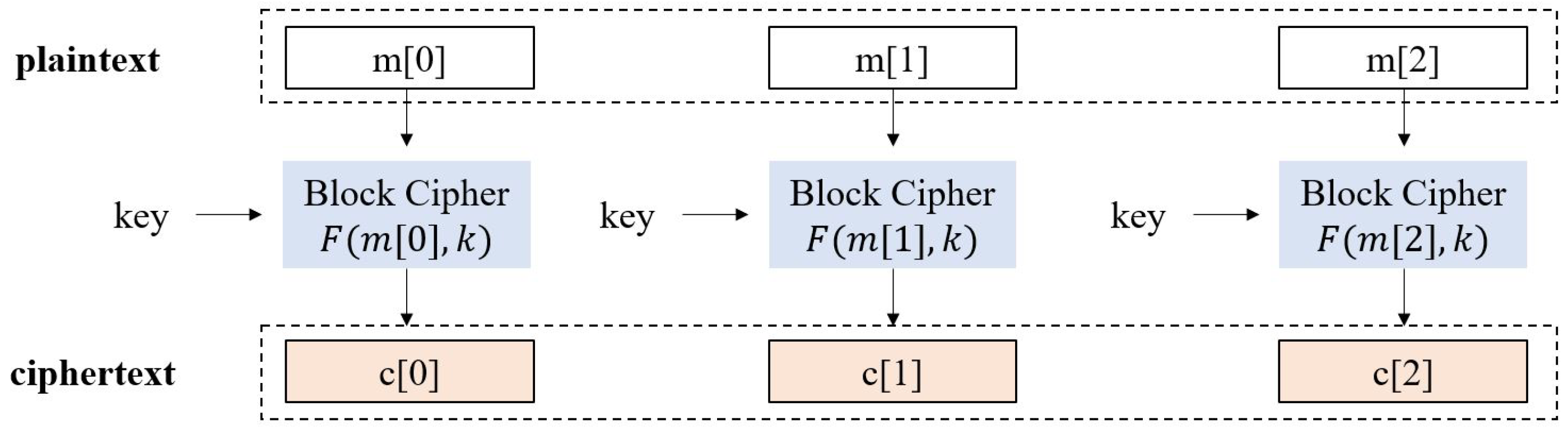
Block cipher in ECB mode is a simple way of encrypting blocks in a message. As shown in
Figure 1, the message is divided into blocks, and each block is encrypted by a cipher algorithm separately. The vulnerability in the ECB mode is that identical plaintext blocks are encrypted into identical ciphertext blocks. It indicates that the ECB mode does not guarantee IND-CPA security, i.e., the attacker can distinguish ciphertexts of the same message. However, the ECB mode satisfies IND-DCPA in which no more information is revealed except that two blocks are equivalent. Most of NVM encryption schemes such as [
5] utilize the ECB mode, since it is simple and does not require any additional memory space. In our scheme we encrypt inert data blocks with the ECB mode while maintaining a symmetric key securely in the processor area.
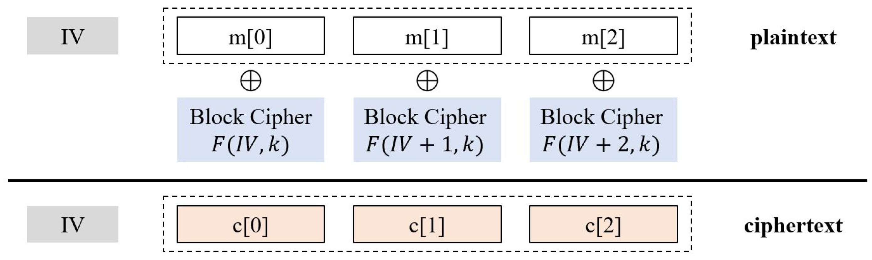
The CTR mode is a representative example for the stream cipher. In the CTR mode, pseudorandom function (PRF) is used to generate a corresponding XOR keystream to encrypt a message, as shown in
Figure 2. When encrypting, a nonce (IV) is randomly chosen and combined with a different counter value for each block. The PRF receives nonce, counter, and symmetric key as an input, then outputs a pseudorandom keystream. Then the message is encrypted by XORing the keystream. Assuming that the PRF generates a uniform string with a different input, the CTR mode guarantees semantic security. Some researches such as [
34] proposed to adopt the CTR mode with using a physical address as a counter. In our scheme we use the CTR mode when encrypting active data with an address, a nonce, and a global key.
The NVM-shelf with two modes provides at least IND-DCPA security: inert blocks with the ECB mode provides IND-DCPA security, and active blocks with the CTR mode provides IND-CPA security. Note that our main focus is on the active blocks, so any encryption can be adopted for the inert blocks. It indicates that it is also possible to gain IND-CPA security in the inert blocks if encrypted with IND-CPA secure scheme, at its own cost.
4. Proposed Hybrid Encryption
In this section, we represent the proposed NVM-shelf: secure hybrid encryption scheme with less flip (shelf) for non-volatile memory (NVM). In
Section 4.1, we first show the main idea and overall construction of our proposed NVM-shelf.
Section 4.2 elaborates on how to decide and classify active blocks.
Section 4.3 defines the modified CTR mode encryption, which we apply to the active blocks.
4.1. Construction
The proposed NVM-shelf is a hybrid encryption scheme, which focuses on reducing the flip penalty of active blocks. The beginning of main idea is that applying the CTR mode with reusing the keystream can avoid the avalanche effect of encryption, due to the property of stream cipher (i.e., XOR operation); when assuming physical attacks, it is secure to reuse the keystream if it can be updated before the next physical snapshot. However, the CTR mode requires a nonce to be stored for each block address, which leads to an additional storage cost. Moreover, large storage forces the nonce to be stored in the off-chip memory, which can be vulnerable to malicious injections and security leakages. We address this problem by applying the CTR mode to the small portion of write-intensive data, which we define as active blocks. Since write-intensive data is mostly responsible for the flip penalty, focusing on the active blocks can cover most of the flip penalty. In this case, the only nonce that needs to be stored is the nonce for the active blocks; it is now possible to store the nonce in the on-chip processor.
To accomplish the idea above, we adopt two modes in the AES block cipher—ECB mode and CTR mode—and modify the CTR mode to reuse the keystream within a period. Our main focus is on the active blocks (i.e., write-intensive data); we apply the modified CTR mode to the active blocks where the keystream update period is configurable by the clock cycles N. Since the CTR mode requires an independent nonce to be stored for each block address, we utilize a flag-table to keep track of active blocks and a timestamp-table to store the memory-write timestamps of active blocks for nonce generation. For the inert blocks, we simply apply the original ECB mode, which does not require any additional nonce storage; but any encryption scheme can be applied instead, at its own cost.
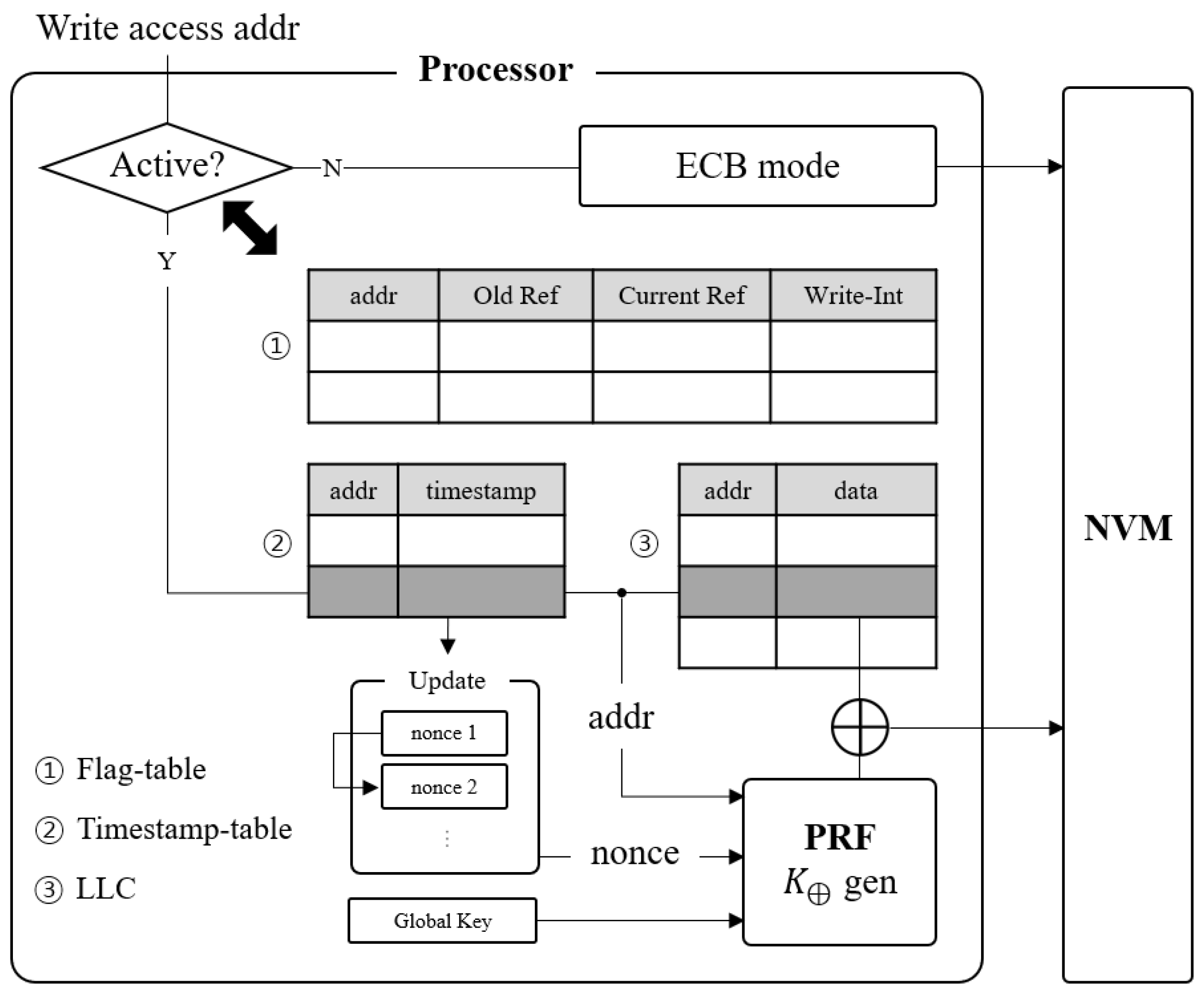
Figure 3 shows the overall outline of the NVM-shelf for a memory-write. When the NVM write is requested, we identify whether the corresponding block is active by utilizing the flag-table. If the block is inert, it is encrypted with the ECB mode. If the block is active we use the modified CTR mode where the keystream is generated by a pseudorandom function (PRF) with address, nonce, and global key as inputs. We utilize the timestamp of memory-write as a nonce: The timestamp-table holds the timestamp of write, which will be updated when data is flushed to the memory. In case of the memory-read, the decryption is operated opposite to the encryption procedure: inert blocks are decrypted by the ECB mode, and active blocks are decrypted by fetching nonce from the timestamp-table and re-generating the keystream.
4.2. Active Blocks
The write-intensive data indicates data that are engaged in frequent memory-writes. In the NVM-shelf, we define write-intensive data as active, and define the active cache lines in the last-level cache as active blocks.
To classify active blocks, we add a flag-table that stores the access information of the data blocks within a period, and devise a table-driven algorithm that can classify active blocks within the update period. Then to hold the updatable nonce for active blocks, we add a timestamp-table that stores the timestamp (clock cycle) of memory-write for each active block address.
Flag-table: The flag-table is a structure array in a processor area that stores three flags corresponding to each block address. It consists of four rows of components as in
Figure 3; block address, Old Reference (OR) flag, Current Reference (CR) flag, and write-intensive (WI) flag. If WI flag is set, the block is determined as active; otherwise it is considered as an inert block. When memory write is requested, a processor searches an address in the flag-table to acquire the WI flag of the block. If there is no information in the table, the address of the block is added to the table and with setting the CR flag (i.e., change the bit to 1).
Initially, all blocks are assumed as inert blocks when the system is booted up. When the block is referenced for frequent write requests, it becomes an active block with setting the WI flag. In the opposite manner, if an inert block seems to have no more memory write access, it becomes an inert block with resetting the WI flag (i.e., changing the bit to 0). The sketch of a classification algorithm is to simply assume that the blocks referred more than once in a period are active, and blocks that are not referred within a period at all are inert. If an inert block is referred for memory write in a period more than once, we anticipate that it will be referred again and set as the WI flag. On the other hand, if an active block was not referred in the previous period, the block is not likely to be referred afterward, so we reset the WI flag.
To determine the write reference of blocks, we define two reference flags—current reference (CR) flag and old reference (OR) flag. Then we update the flag-table in the beginning of each update period. CR flag is set when it is referred in the current refresh period. When the period ends, CR flag is copied to OR flag. Then CR flag is reset for a new period. In this way CR flag will always contain the current period reference, and OR flag will contain the previous period reference. Algorithm 1 defines how to manage the flag-table.
| Algorithm 1: Flag-table reference. |
![Electronics 09 01304 i001]() |
When a cache block is written or flushed in a main memory, a processor first checks if the address tag for the cache block exists in the flag-table. If the address does not exist, we insert a row for the address and set the CR flag. If the address already exits, the processor checks reference flags to decide the WI flag of the corresponding block. If the CR flag is set and WI flag is not, then the block becomes active, since it is referred twice in a same period. In the case when OR flag of the active block (i.e., WI flag is set) is false, the block becomes inert since the block was not referred during the previous period. By following the algorithm, blocks are categorized into active and inert blocks. In this setting, the processor observes the WI flag to decide which encryption algorithm is applied for the memory write—PAD encryption for active blocks and AES block cipher for inert blocks.
Timestamp-table: We add another feature called timestamp-table, a structure array that lies in a processor area to store the latest clock cycle timestamp of each active block address when memory write is requested. As in
Figure 3, the timestamp-table consists of two rows; block address and timestamp. We utilize this distinct timestamp to create the periodically evolving nonce, which is used for the keystream generation.
Re-encryption: The size of flag-table and timestamp-table is limited, and the eviction due to the missed address may cause an additional re-encryption cost. Since we apply different encryption schemes for active blocks and inert blocks, the type change from active to inert block also requires the change of encryption. Namely when the active block is evicted from the timestamp-table or flag-table, we need to first decrypt the corresponding block with the CTR mode, and encrypt it again with the ECB mode.
Algorithm 2 shows the replacement procedure of the timestamp-table. When a block is evicted from the timestamp-table, the timestamp is no longer valid for the corresponding block. Hence the block cannot stay as an active block anymore, which requires the re-encryption phase. In the case of the flag-table eviction, the block may also need re-encryption if the WI flag was set (i.e., active block) for the corresponding line.
| Algorithm 2: Timestamp-table replacement. |
![Electronics 09 01304 i002]() |
4.3. Proposed CTR Mode
We design a novel version of CTR mode encryption, by modifying the CTR mode in the AES block cipher. The proposed CTR mode is applied to the active blocks, where the keystream is reused within the update period denoted as N. The original CTR mode in the block cipher utilizes the AES block cipher as a pseudorandom function (PRF) to generate the keystream, where the PRF takes a key, IV, and a counter as inputs. While IV and counter are regarded as nonce in the original CTR mode, we specifically replace this nonce with an updatable value to achieve the periodic keystream update. In this manner, we utilize three inputs for the PRF as follows:
Global key (G): A secret key in a processor area, which cannot be extracted (e.g., secret key from TPM).
Block address (P): An address of the block, to generate distinct keystream for each block (i.e., spatial exclusivity).
Temporal nonce (): It is a nonce value by dividing the timestamp of memory-write (n) by the update period (N).
With these inputs, the PRF outputs the keystream which is XORed with the plain data for encryption. Formally, for each memory-read/write access, a keystream for the corresponding block denoted as
is generated as follows:
where
G = global key,
P = block address,
n = timestamp of write,
N = update period, and
concatenates strings.
The
output size is digested equal to the original data in a block, and we use an XOR operation of data and
for both encryption and decryption. The timestamp (
n) is stored in a table when encrypting to the NVM, and fetched again when decrypting from the NVM; we can generate the same
for each encryption/decryption pair. Since
is equivalent for each pair, the encrypted ciphertext is decrypted correctly as follows.
Note that global key (G), update period (N), block address (P) are fixed values. The only evolving value is the timestamp (n) of the write request. When observing the calculated nonce (), the nonce does not change until n reaches a multiple of N. Accordingly the PRF output also does not change. Thus the PRF output remains the same within the update period (N), and is updated at the beginning of each period; we can reuse the within the update period as intended.
4.4. Cache-Based Experiments
In this section, we present the experimental results of the proposed NVM-shelf framework. We implement our NVM-shelf by modifying the cache hardware, based on the timed-QEMU simulator TQSIM [
15]. For the evaluation, we utilize some applications from Mibench [
35] with distributing random and sequential examples fairly. We also evaluate some applications from the PARSEC [
36] benchmark.
We mainly observe the flip penalty, active block detection, update period, and the consequence of table size. For the default configuration, we leverage a unified, eight way set-associative cache, with LRU policy and size of 8192 lines (64B for each line). As described in
Section 4.1, we encrypt all blocks where the blocks are categorized as two types: inert blocks and active blocks. For the inert block encryption, we use the AES block cipher in ECB mode (AES-128-ecb) from openSSL, and for the PRF we also use the same AES function as in the CTR mode. Since AES is a keyed function unlike the PRF, we let the global key
G work as a secret key of the AES encryption. Specifically, we set the keystream
as
, instead of
. The default update period is 1
s, and the timestamp cache is a single line of 14B. Flag-table contains four lines, 4B for each line. Note that we compare the NVM-shelf to the whole encryption which encrypts the entire blocks with an AES block cipher.
4.4.1. Flip Penalty
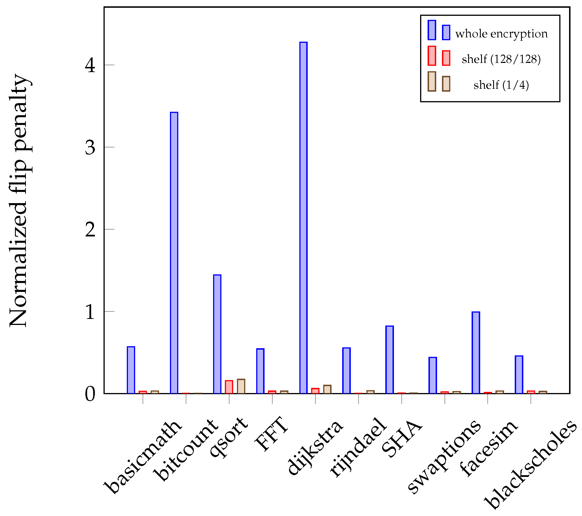
Figure 4 compares the number of flipped bits in the whole encryption approach with our NVM-shelf for each application. The
y axis represents the additional number of flipped bits normalized by the original flips with no encryption. In the figure, shelf (1/4) denotes that the timestamp cache has a single line, and the flag-table has four lines. Similarly in shelf (128/128), there are 128 lines in the timestamp cache and the flag-table, respectively.
In the whole encryption, the flip penalty is completely unpredictable, since the data is entirely randomized. Therefore, the flip penalties of whole encryption are entirely unrelated to the application. On the other hand, the NVM-shelf tends to show better performance in sequential applications (many sequential memory accesses) such as bitcount, since reusing the keystream can be much more beneficial in the applications with spatial or temporal locality. Even for the random applications (many random memory accesses) such as swaptions, the NVM-shelf still shows much better performance compared with the whole encryption.
On average, the NVM-shelf with 128 cache lines, 128 flag-table lines, and update period of 1 s only has 3% of flip penalty, i.e., only 3% of bit flips are increased compared with the no encryption approach. On the other hand, the whole encryption approach has 135% of flip penalty on average, compared with the no encryption.
4.4.2. Active Blocks
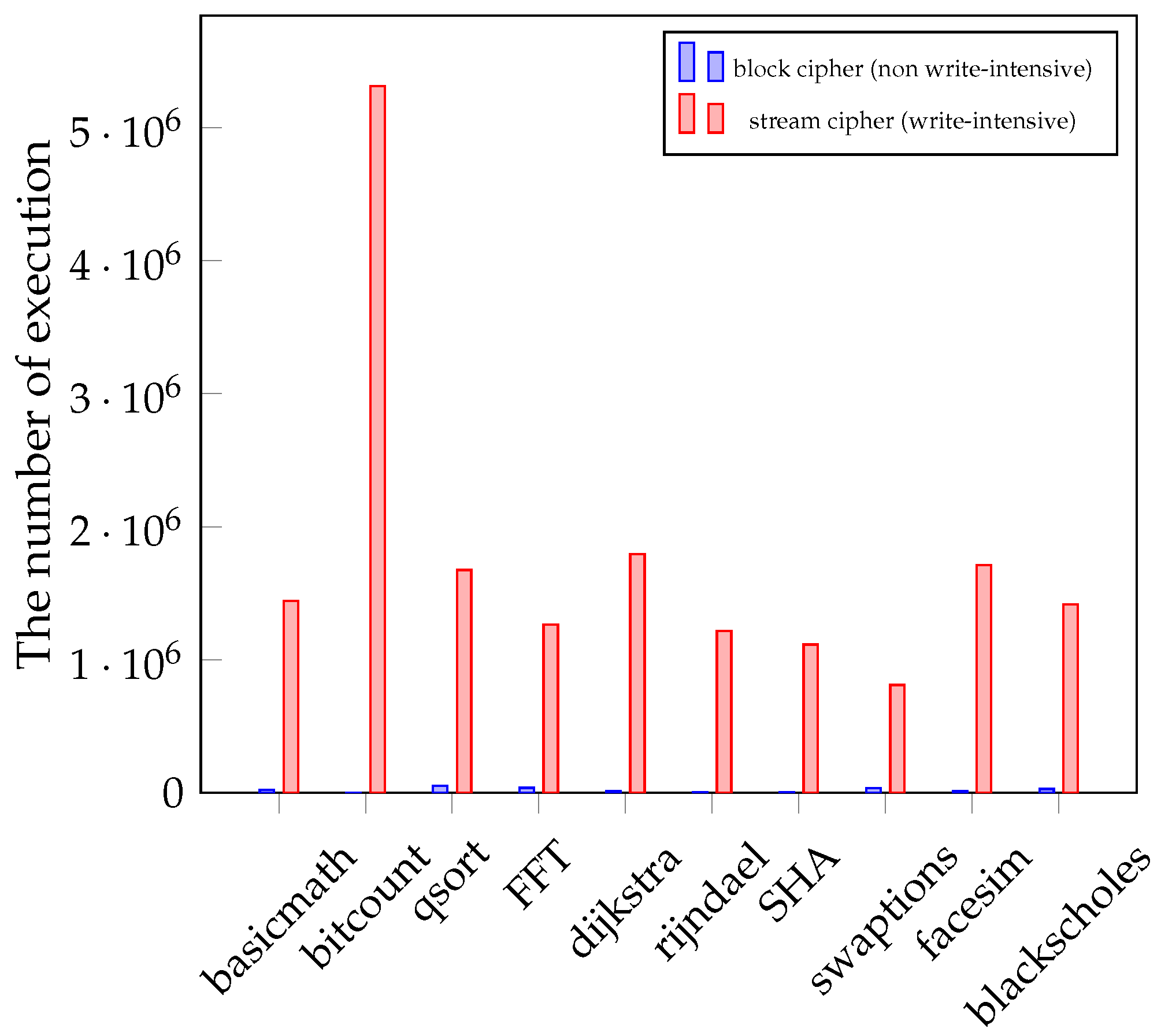
We measure how many times the PAD encryption and AES encryption are performed, to observe the occupation of active blocks.
Figure 5 shows how many times the AES encryption and the PAD encryption are performed in each application. As shown in the figure, the PAD encryption is called much more frequently than the block cipher in the proposed NVM-shelf. It means that active blocks have temporal/spatial locality and are classified as an active block even with small sized timestamp cache and flag-table.
4.4.3. Update Period
Figure 6 shows the number of flipped bits in the hybrid scheme by varying update period
N with 1
s, 1 ms, and 1 s. In simulation, since we assume that a processor cycle is 1 GHz, the update period cycle is
,
, and
, respectively. Therefore, shelf (
), shelf (
), and shelf (
) indicate that the key is updated every 1
s, 1 ms, and 1 s, respectively.
As in the figure, when the update period N is set as 1 s, the flip penalty is relatively high; the period is too short to gain the benefit of the temporal locality of the application process. When the update period N is set as 1 ms, it shows almost similar flip penalties compared with 1 s in all applications, which indicates that 1 ms is enough to reflect the benefit of the hybrid encryption in general.
4.4.4. Timestamp Cache and Flag-Table Size
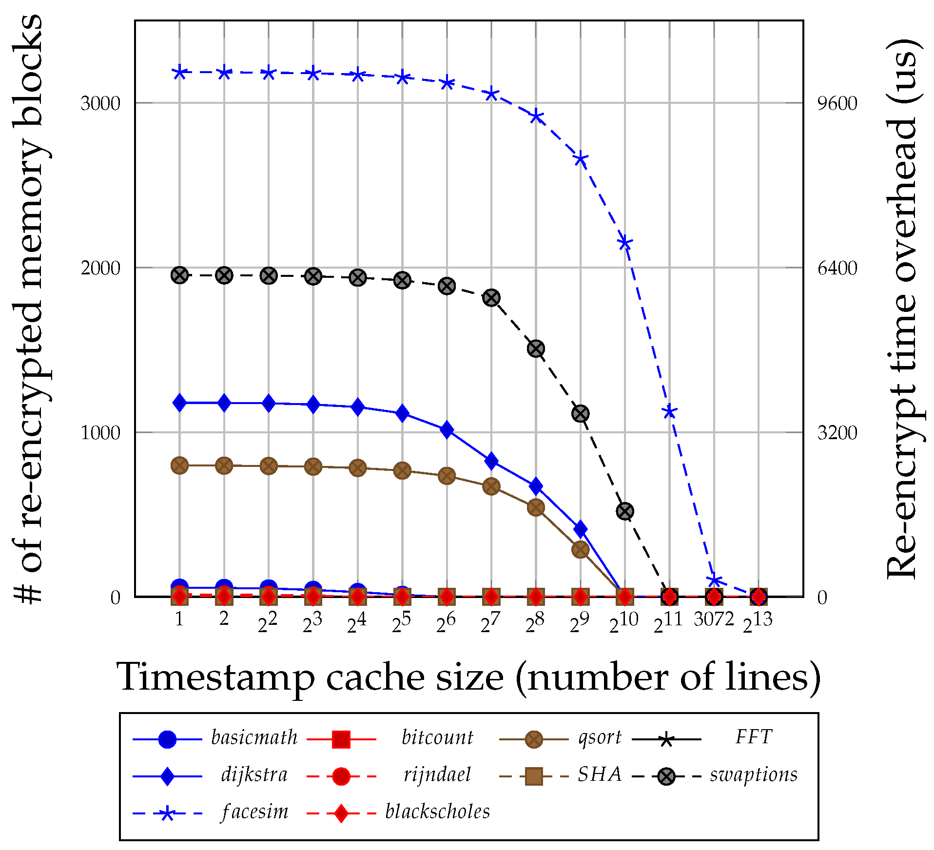
Figure 7 shows the number of recrypted blocks by varying the timestamp cache size. The
x axis represents the number of lines in the timestamp cache, and the
y axis denotes the number of recrypted NVM blocks. The applications without random write operations require a small number of recrypt operations while applications with many random write operations such as facesim, swaptions, dijkstra, and qsort require recrypt operations frequently. As the timestamp cache size increases, the number of timestamp cache replacements and the number of recrypted blocks decrease. In each recrypt process, the system reads the block from memory, decrypts it with PAD, encrypts it with a block cipher, and writes the block into memory. The graph shows the performance overhead caused by the recrypt with assuming that the recrypt process takes 3.2
s (3200 cycles), on a 1 GHz machine approximately.
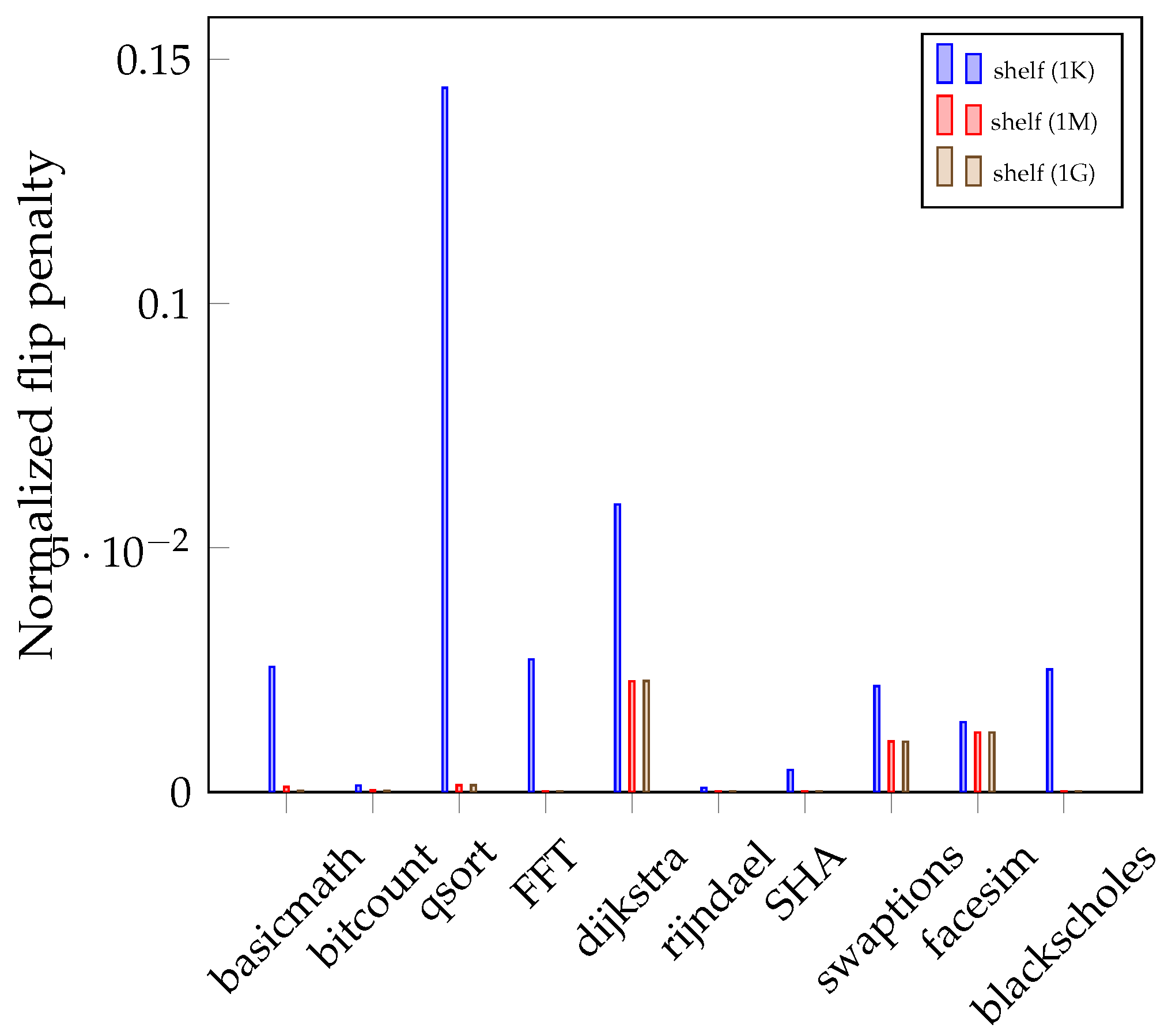
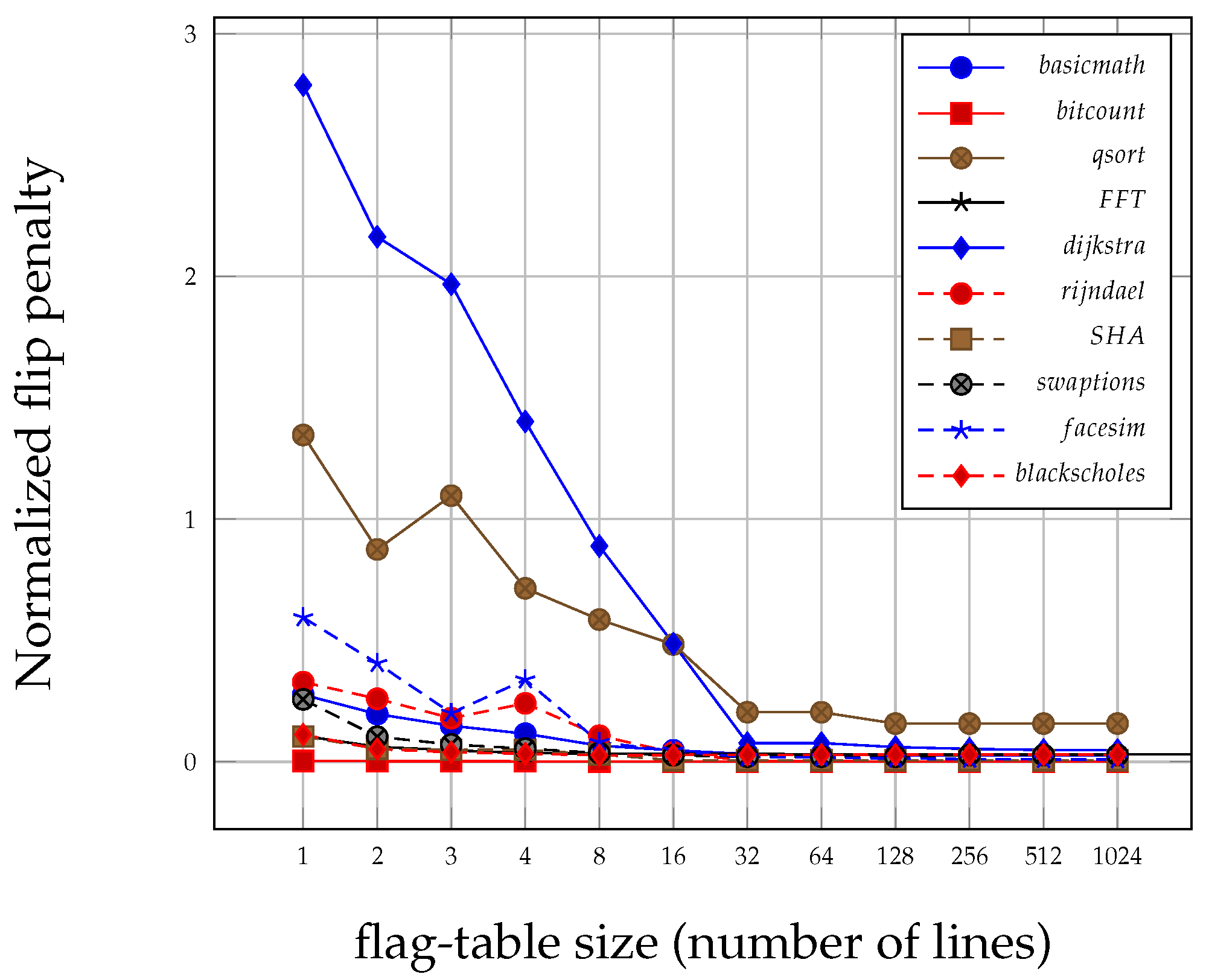
Figure 8 shows the flip penalty by varying the flag-table size. Similarly, the
x axis denotes the number of lines in the flag-table, and the
y axis presents the flip penalty normalized by no encryption approach. As the flag-table size increases, more data blocks are classified as active so the number of flipped bits decreases. Actually, if there are 32 lines in the flag-table then the number of flipped bits is saturated. Consequently, a timestamp cache with a single line and a flag-table with 32 lines can reduce the number of flipped bits dramatically in many applications.
5. SA-SPM Compiler
To implement the NVM-shelf framework, it is required to modify the hardware cache to support the algorithm. When assuming SPM-based systems instead of cache-based systems, it is possible to apply NVM-shelf without modifying any hardware structures since SPM itself is managed by the software. However, to achieve the NVM-shelf in the SPM-based system, the first requirement is to let the SPM support at least AES block cipher encryption of the main memory. It is non-trivial to encrypt all memory segments located in the global memory in the SPM-based architecture, since the SPM management itself has its own fixed logistics. Some existing approaches [
37] try to integrate the SPM management with encryption but have not succeeded in providing holistic encryption of data in global memory, leaving parts of the memory content in plaintext. Therefore, before implementing the NVM-shelf framework, it is important to devise an SPM-aware compiler which can support encryption for the entire memory region.
We introduce our novel SPM compiler referred to in this paper as Security-Aware Scratch-Pad Memory (SA-SPM). It primarily integrates the encryption/decryption phase into the SPM management scheme. Furthermore, the proposed compiler ensures the holistic protection of global memory data segments (including stack, heap, code, and static variables). The constituents of this SA-SPM compiler framework include: (i) a cluster of code optimization and transformation passes, (ii) a run-time management kernel, and (iii) an augmentation tool for SPM-aware executable code.
Code optimization and transformation pass leverage the well-known LLVM [
38] source code compilation tool-chain. Using this tool-chain, we initially compile the subject/user application source code to the LLVM intermediate representation bytecode (LLVM-IR). Henceforth, our proposed SA-SPM code optimization and transformation pass run a set of analysis and augmentation processes on the LLVM-IR and ultimately transforms the SPM oblivious user application to an SPM-aware code with the proper insertion of run-time management kernel functions.
Run-time management kernel implements the core SPM management mechanism. It transparently manages all memory segments (including the heap, stack, and code) with the proper procedures to fetch and evict data between the SPM and the global memory. These procedures integrate the necessary encryption/decryption phases to support the proposed hybrid encryption scheme.
Executable file/code augmentation tool protects with prior encryption any sensitive contents such as the read-only application code and pre-allocated static variables.
Combining these components, our proposed SA-SPM compiler takes an arbitrary user source code and transforms it into an SPM aware executable code with or without global memory encryption.
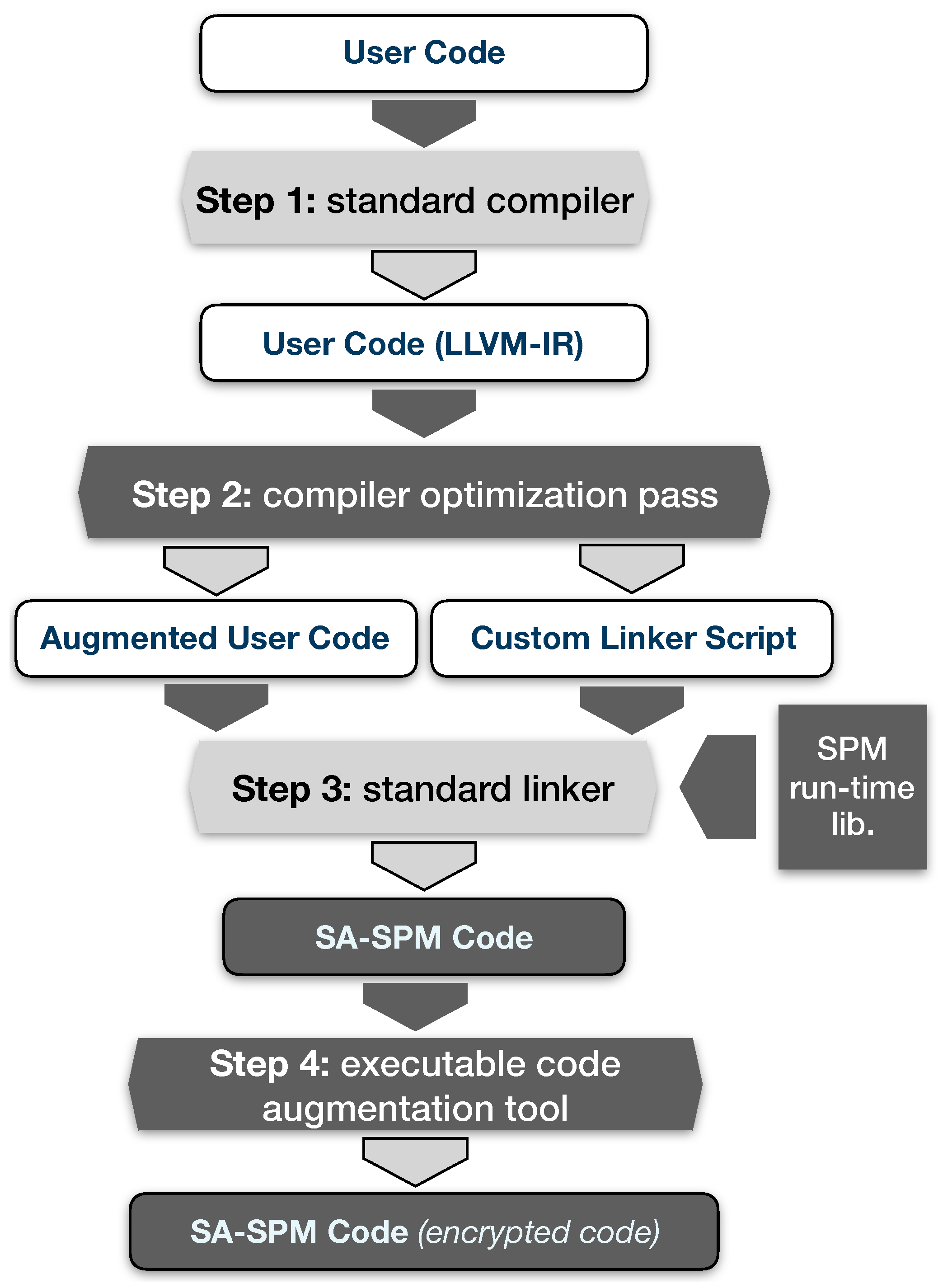
5.1. SA-SPM Code Generation Flow
Figure 9 illustrates a summary of the code transformation procedures for generating an SPM-aware application. The following elaborates further on each of these procedures.
Step 1: We utilize the source code (e.g.,
C source code) compiler program shipped with LLVM [
38] tool-chain to generate the corresponding LLVM-IR bytecode from the original subject/user application.
Step 2: We engage the code optimization and transformation pass in this step to analyze, modify, insert SPM management kernel functions into the original LLVM-IR, and generate a linker-script. The custom-generated linker-script guides the shipped binary object code linker program to properly place the various memory segments into the limited SPM size.
Step 3: We utilize the standard linker program to produce an SA-SPM code. The inputs at this step are the augmented user code, the generated linker-script and the SPM run-time management library.
Step 4: The SA-SPM code package is secured with the executable code augmentation tool by encrypting only the sections where predefined user variables and instructions are located.
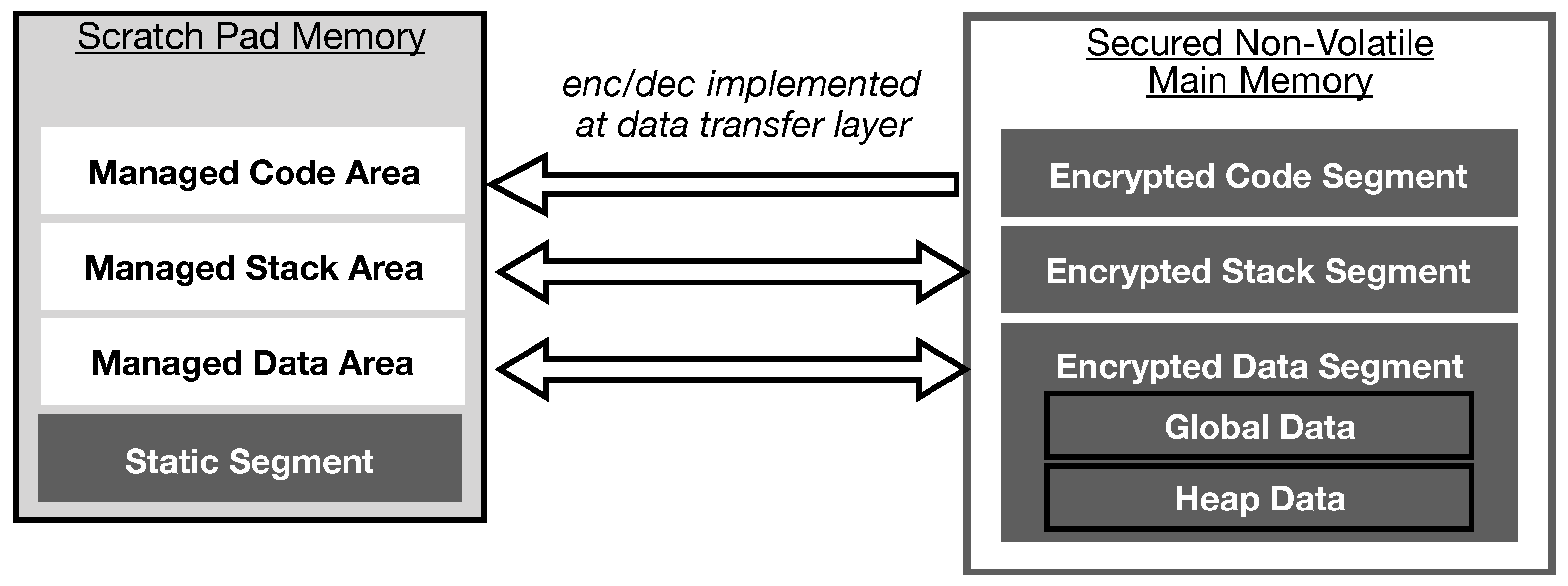
As mentioned above, the run-time management kernel integrates the proposed hybrid encryption/decryption implementation. This implementation ensures data from the stack and heap are encrypted prior to eviction to global memory and decrypted when fetched back to SPM. In the case of application code/text which is read-only data, we encrypt this data segment only once in step 4 of the application generation steps enumerated above. Therefore, during execution, no eviction and encryption are necessary for code/text data.
Figure 10 illustrates the aftermath of the proposed scheme. All data located in the global memory becomes meaningless to an attacker, albeit successful and unauthorized acquisition of data. The following sections elaborate further on the SPM management mechanism adopted for each memory segment.
5.2. Heap Data Management
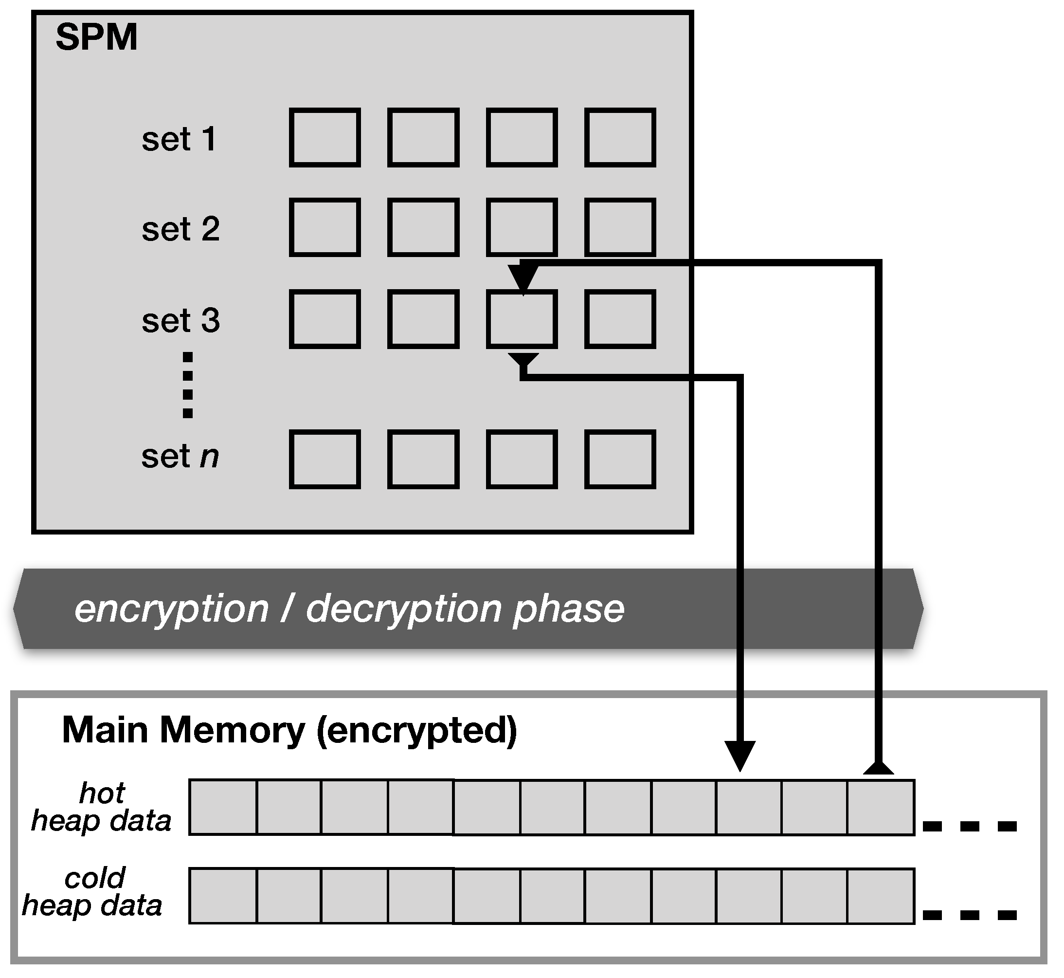
In this paper, we employ a dynamic management scheme with fixed data blocks for managing heap memory segment. This scheme depicts the hardware cache management scheme where a data block is fetched or evicted at run-time. In
Figure 11, we illustrate an example structure for heap management. All sets contain an adjustable and equal number of data blocks. This is referred to as the
n-way set-associativity. The structure is then populated with the maximum number of sets that can fit in the SPM memory space allocated for heap management.
Figure 11 shows a 4-way set-associative structure. In step 2 of the flow illustrated in
Figure 9, the proposed code optimization and transformation pass inserts function call instruction before access to heap data instruction in the original user code. The inserted function call invokes a run-time management kernel function—(global_2_local). This function ensures the block containing the heap data is present is the SPM, and if necessary, evicts an existing block to free up space prior to fetching the requested block from global memory. The global_2_local function returns the SPM (local) address where the requested data have been placed. For the eviction process, this paper adopted the least recently used (LRU) or round-robin evicted policy and applied it to each set separately.
Figure 11 illustrates how the fetch/eviction process encompasses our hybrid encryption/decryption scheme implementation. Note that the global_2_local function call and address translation is applied only to variables in the heap segment to mitigate the performance penalty, and this is not required for stack and static variables.
5.3. Statically Allocated Variable (Global Data) Management
We propose a two-way approach to managing statically allocated variables. First, we classify them into most frequently and less frequently accessed variables. We achieve this by utilizing a profiling approach, which generates variable access counts. Then the frequently accessed variables are appended to the SPM static segment as long as there is enough free space. After that, we prepend any remaining variables not placed in SPM due to size limitation to the global memory heap segment. This approach implies that the heap management scheme mentioned in
Section 5.2 then becomes the manager for the remaining static variables. Placing the frequently accessed static variables in SPM aid in mitigating the management overheads since they will be fetched and decrypted once at application lunchtime.
5.4. Code/Text Data Management
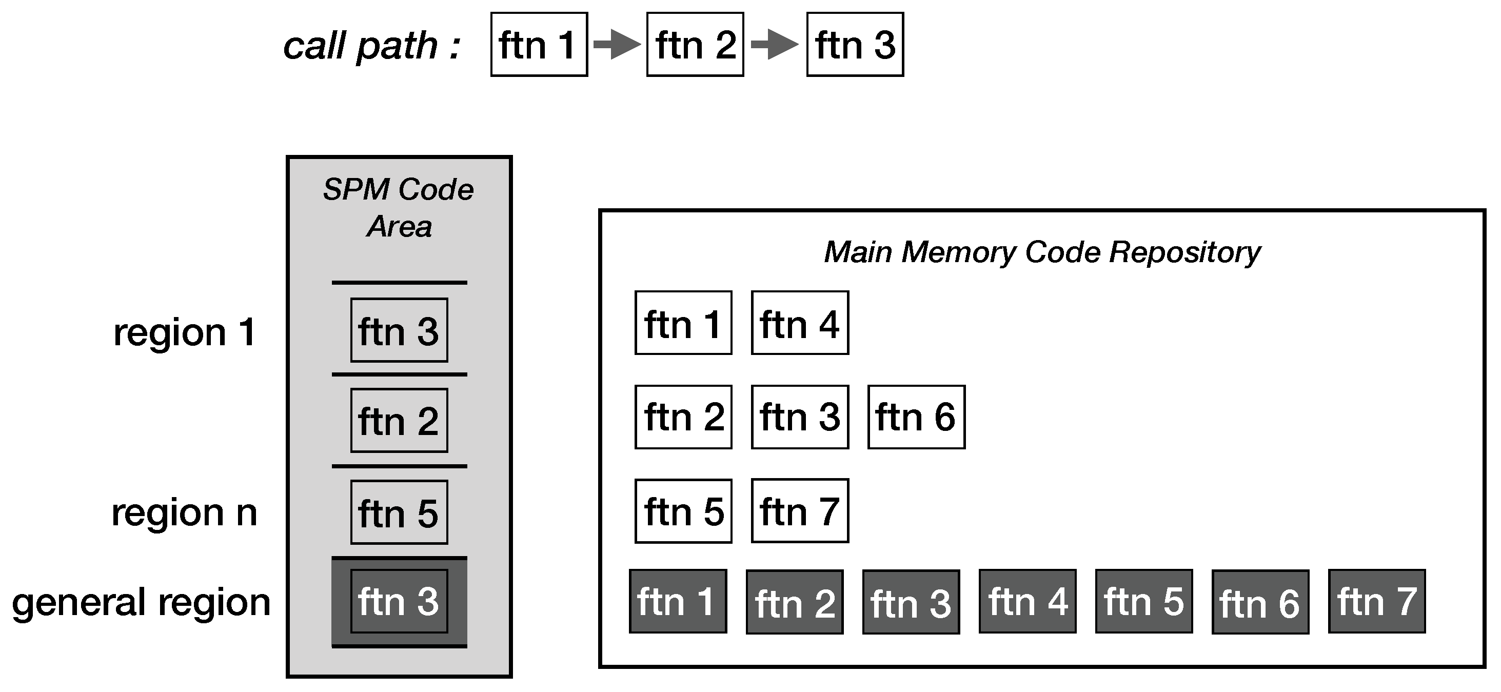
In this work, we extended the existing work proposed by Bai et al. [
37]. In their work, they divided the SPM memory range allocated for user code/text into sub-regions. Each sub-region will hold a user function selected from a designated functions group. Therefore, at any point in the execution process, only one function from a function group will be present in the sub-region. Similarly, the proposed code optimization and transformation pass attaches a function call wrapper to user function call instructions. The invoked run-time management kernel function—(fcallee_wrapper), likewise, ensures the callee function is fetched and decrypted from the function group located in global memory to the sub-region in SPM.
In their work [
37], only one user function from a particular function group will be present is SPM at any given time. This approach may result in a high-performance penalty if both the caller and callee functions belong to the same function group causing double code fetch and decryption procedures for that single function call. In this paper, we propose the general sub-region to limit this eventuality. With reference to
Figure 12, the general sub-region can hold any user function including the immediate caller function such that the callee function can return immediately without incurring an additional fetch procedure. This work can realize this situation through the use of function replication. All user functions are replicated with the second copy using the general sub-region as the function entry address. The figure shows the many-to-one global function group to SPM code sub-region organization described in [
37] as well as our proposed user function replication and the general sub-region. The code optimization and transformation pass ensures the replicated function uses the general sub-region as the start address and generates the proper linker script. All encrypted user functions can be stored in any location in the global memory as long as the CPU core is not directly loading instructions from the global memory. Only the run-time management kernel is required to be aware of the global memory addresses for all user functions to guarantee the fetch procedure accuracy.
5.5. Stack Data Management
This paper employed and extended the scheme proposed by Lu et al. [
39] to manage stack data. The scheme fundamentally ensures the current free space in the SPM stack segment is large enough to accommodate the entire stack frame for the callee function. Otherwise, stack frames belonging to previous caller function(s) and currently held in SPM are evicted and encrypted prior to entering the callee function. Conversely, before returning to the caller function, the appropriate run-time management kernel function fetches and decrypts the caller stack frame from global memory. For this [
39] scheme, the code optimization and transformation pass needs to acquire information about the user application’s call-graph, call depth, and stack frame sizes in order to determine the least number of run-time eviction function calls needed the prevent SPM stack segment overflow.
In a situation where acquiring this information is not successful, our proposed code optimization and transformation pass inserts instructions to check the available stack size and if necessary invoke the run-time management kernel function to perform eviction procedures before entering the callee function. These inserted instructions are carefully tailored to minimize the performance penalty.
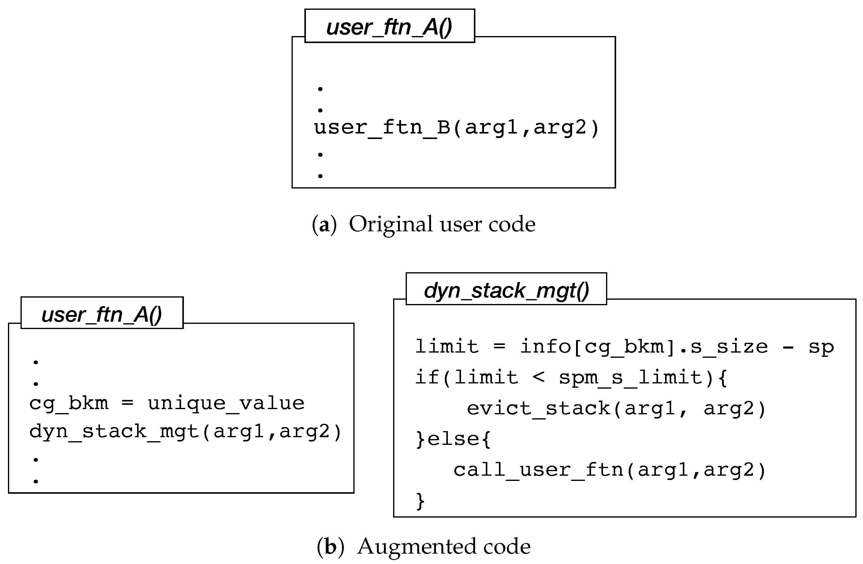
Figure 13 presents an excerpt of a sample user code and its SPM-aware transformed code.
Figure 13a shows the original user code in which the caller function user_ftn_A() calls the callee function user_ftn_B(). During SPM-aware code compilation, the code optimization and transformation pass replaces this original user code with an instruction to invoke the run-time management kernel function dyn_stack_mgt() as illustrated in
Figure 13b. This function verifies the availability of SPM stack space and decides if caller stack frame eviction is required. With respect to the inserted instruction (cg_bkm = unique_value), the dyn_stack_mgt() function can determine and directly invoke the user’s callee function. With this approach, callee function will return into the dyn_stack_mgt() function such that the caller stack frame can be restored before returning to it. In this work, we implement parts of the dyn_stack_mgt() function with assembly code to reduce the performance penalty. This enables the function to execute only nine instructions, with three of them being memory access instructions (LOAD/STORE) in the case where caller stack frame eviction is not necessary.
We discuss in the following sub-sections code sanitation procedures applied to the user code to aid in generating SPM-aware code.
Section 5.5.1 and
Section 5.5.2 introduce two problems that can hinder smooth code transformation.
Section 5.5.3 then presents a proposed solution.
5.5.1. Problem 1: Large Stack Allocation
Out-of-the-box compilers do not consider if a is cap placed on a function’s stack frame size. Therefore, existing software can allocate large objects such as arrays in the stack frame. However, in embedded systems, SPM memory is limited, making it impossible to execute such functions.
5.5.2. Problem 2: Out-of-Scope Stack Variable Referencing
Likewise, compilers do not consider the existence of a condition where a governing system swaps out parts of application memory space from the primary memory. As such, compilers make no provision to avoid access to memory areas swapped out from the primary memory. The user code can then reference objects allocated in a stack frame belonging to a caller function up in the call-graph. It is rather common practice for user code to pass the address of an object allocated in its stack frame as arguments to callee function(s). Since the proposed SPM management scheme evicts or swaps out caller stack frames, it is erroneous to access the previous stack frame object.
5.5.3. Solution: Stack to Heap Migration
We propose a viable solution to aid alleviation of the problems discussed in
Section 5.5.1 and
Section 5.5.2. The main strategy in this solution is to migrate stack objects that incur these problems to heap allocations. This puts them under the proposed heap management scheme presented in
Section 5.2. Since the heap segment is virtually unlimited, objects can be read or written to at random locations and by any function regardless of the allocating function. Our proposed code optimization and transformation pass includes the feature to identify and effectively migrate these stack objects. The necessary code transformations are as follows: (i) eliminate the stack allocation in the function, (ii) insert heap allocation (malloc) and deallocation (free) at the beginning and end of the function respectively, and (iii) update all references (including function call arguments) to the deleted stack allocation to the new heap allocation.
5.6. SPM-Based Experiments
Based on the SA-SPM compiler, it is now available to plug-in the NVM-shelf framework to the SPM-based systems. In this section, we represent the experimental results by implementing the proposed SA-SPM for the ARM 32-bit processor architecture using LLVM, and integrating the NVM-shelf algorithm from
Section 4. The whole system is simulated based on the Gem5 simulator [
19] full system mode to acquire realistic performance metrics. We devised a Gem5 SimObject that emulates the NVMM with the DCW feature. It generates the total bit flips that have occurred in the device. Another SimObject to make performance measurements. Original user programs were taken from a benchmarking application suite (MiBench). For the evaluation, we utilize the applications from Mibench similar to the cache-based experiment. The applications must go through major modifications to be compatible with the SPM environment, i.e., to be aware of the SPM memory access control. Some applications are not available to be modified at all: for example, if the application includes some mathematical libraries which are not implemented in the SPM, it cannot be modified to be compatible with the SPM environment. Therefore, the selection of applications is slightly different from the cache-based experiment. First, we will present the experimentation setup, then, we show the performance overhead, and finally discuss the bit-flip that occurred during the execution of various encryption schemes.
Table 1 presents the experiment default configurations. We configured the heap management to use a four-way set-associative organization with a block size of 128 bytes, eight sets, utilizing 4 Kilobytes of SPM area, and a round-robin eviction policy.
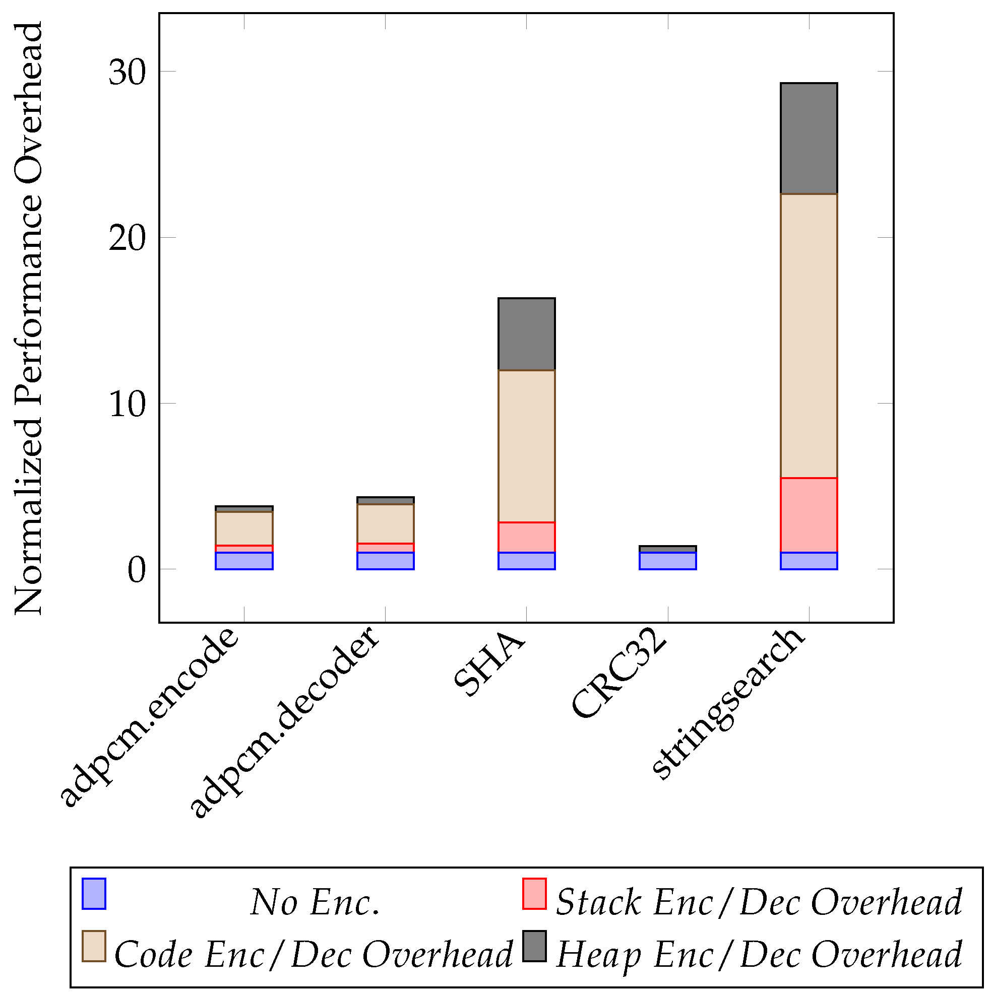
Figure 14 shows the performance penalty (normalized by the no encryption) incurred by the run-time management kernel functions for managing each of the memory segments. It can be observed that the SHA and stringsearch applications had higher performance penalty due to large numbers of function calls. This resulted in several fetch processes. The integrated decryption in the fetch process represents the largest penalty.
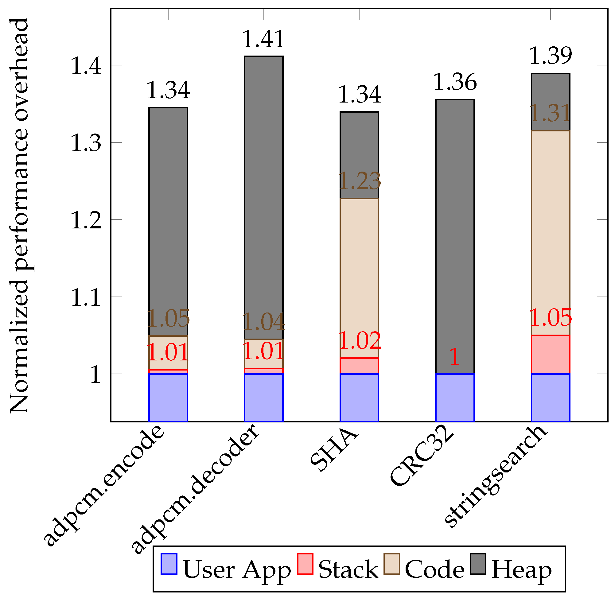
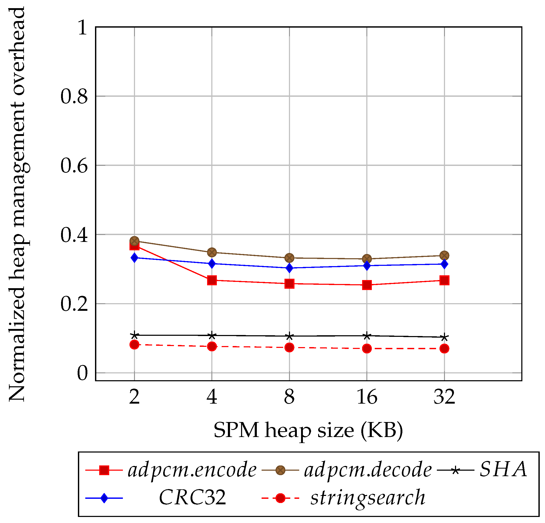
Figure 15 shows the run-time management kernel overheads without the encryption/decryption phase for each memory segment. We normalized it by the execution time of the original user code. The results show that the run-time management kernel introduces a 41% performance penalty for the worst-case scenario. Another observation is that the stack management introduces no more than 5% overheads for all benchmark applications, a fact attributed to the migration of large stack objects to the heap segment.
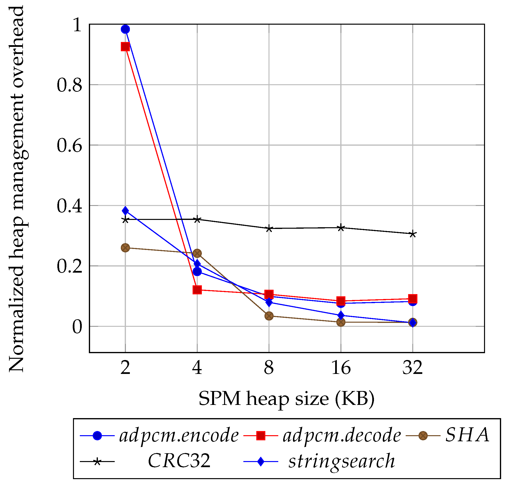
Figure 16 shows the isolated performance overheads introduced by the encryption/decryption phase integrated into the heap management. We vary the SPM heap segment size starting from 2 Kilobytes to 32 Kilobytes. Note that
Figure 14 is a special case of
Figure 16 where the SPM heap segment is 4 Kilobytes. As an example, encryption/decryption execution time for the stringsearch application requires about 20% of the overall execution time in the heap region.
Figure 17 also shows the isolated performance overheads introduced by the heap management but without the encryption/decryption phase, and normalized to the application total execution time. Similarly, we vary the heap segment size (2–32 KB).
Figure 15 is a special case of
Figure 17 where the SPM heap segment is set to 4 Kilobytes.
Table 2 list the total number of SPM heap (including large global and stack objects) block hit, misses, and evictions. Block hits indicate the situation where data accessed by the CPU is present in an SPM heap data block. Miss is the opposite of block hit, which invokes the fetch process with or without prior eviction. Eviction occurs when the content of a victim data block is newer than that of the global memory.
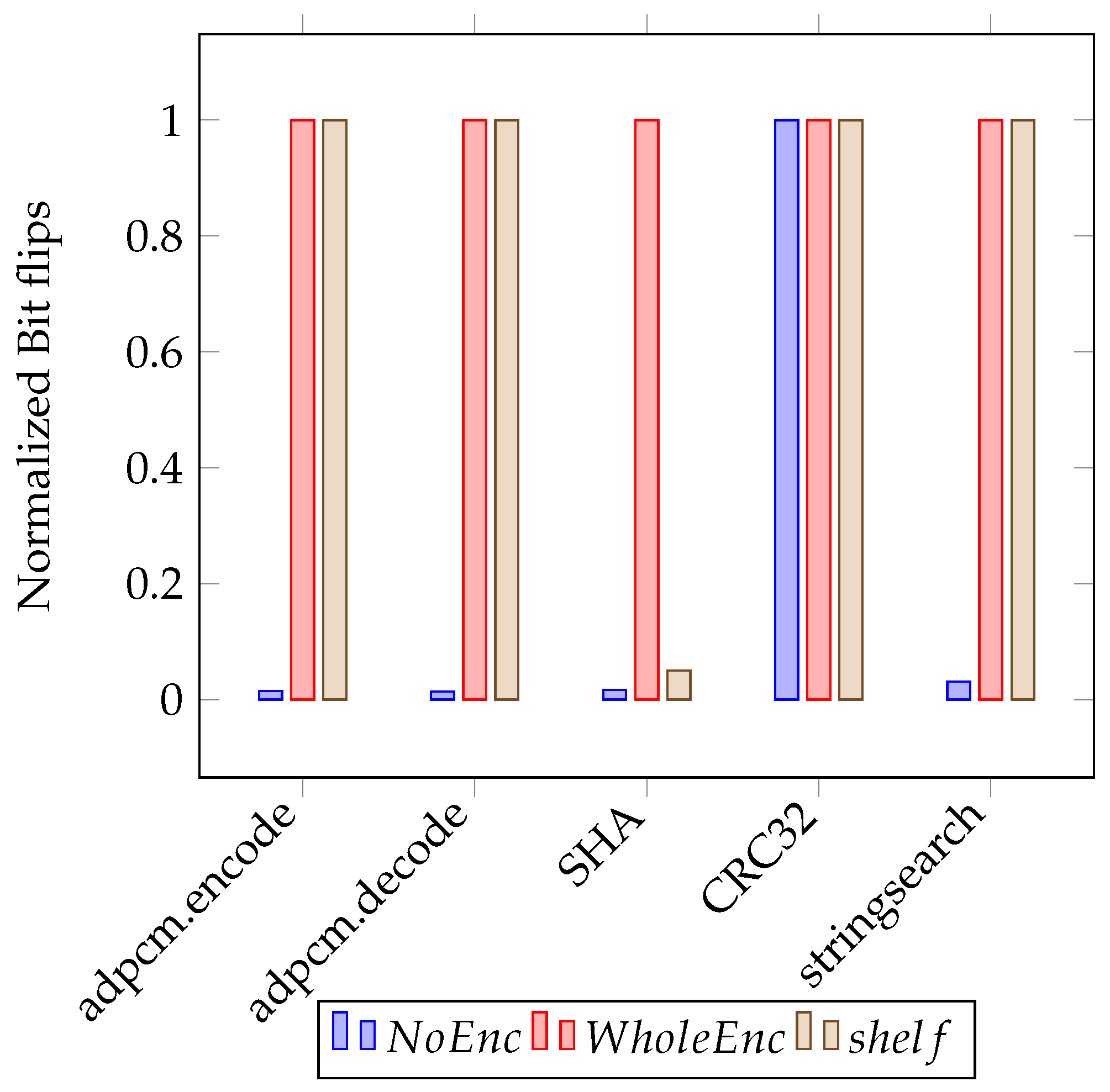
Figure 18 shows the total number of NVMM cell flips (collected by the Gem5 NVMM SimObject) normalized by no encryption mode. Observe that the NVM-shelf is useful in SHA application, which has many SPM evictions. The NVM-shelf reduces the number of bit flips by 31.8% compared with the whole encryption.


