Article

Oxide-Electrolyte Thickness Dependence Diode-Like Threshold Switching and High on/off Ratio Characteristics by Using Al2O3 Based CBRAM

1
Thin Film Nano Technology Laboratory, Department of Electronic Engineering, Chang Gung University, 259 Wen-Hwa 1st Rd., Kwei-Shan, Tao-Yuan 33302, Taiwan
2
State-Key Lab for Electronics Material & Research of Ministry of Education of China, Xi’an Jiaotong University, Xi’an 710049, Shanxi, China
3
Department of Obstetrics and Gynecology, Keelung Chang Gung Memorial Hospital (CGMH), No. 222, Maijin Rd., Anle, Keelung 204, Taiwan
*
Author to whom correspondence should be addressed.
Electronics 2020, 9(7), 1106; https://doi.org/10.3390/electronics9071106
Submission received: 27 April 2020 / Revised: 25 June 2020 / Accepted: 3 July 2020 / Published: 7 July 2020
(This article belongs to the Special Issue Challenges and Applications of Non-volatile Memory)

Abstract

:
Diode-like threshold switching and high on/off ratio characteristics by using an Al/Ag/Al2O3/TiN conductive bridge resistive random access memories (CBRAM) have been obtained. The 5 nm-thick Al2O3 device shows superior memory parameters such as low forming voltage and higher switching uniformity as compared to the 20 nm-thick switching layer, owing to higher electric field across the material. Capacitance-voltage (CV) characteristics are observed for the Ag/Al2O3/TiN devices, suggesting the unipolar/bipolar resistive switching phenomena. Negative capacitance (NC) at low frequency proves inductive behavior of the CBRAM devices due to Ag ion migration into the Al2O3 oxide-electrolyte. Thicker Al2O3 film shows diode-like threshold switching behavior with long consecutive 10,000 cycles. It has been found that a thinner Al2O3 device has a larger on/off ratio of >108 as compared to a thicker one. Program/erase (P/E) cycles, read endurance, and data retention of the thinner Al2O3 oxide-electrolyte shows superior phenomena than the thicker electrolyte. The switching mechanism is also explored.

1. Introduction

The challenges faced by conventional flash memories can be overcome by introducing alternative non-volatile memories (NVM) [1]. Lots of emerging NVM devices, such as phase changeable memory (PCM) [2], magnetic random access memory (MRAM) [3], ferroelectric RAM (FeRAM) [4], resistive random access memory (RRAM) [5], conductive bridging random access memory (CBRAM) [6], and so on, are investigated since several decades to fulfill the criteria of nanoscale memory technology. These alternative NVMs have several exciting features, such as (i) physical size reduction, (ii) good endurance characteristics, (iii) longer retention, and (iv) low power consumption [7]. CBRAM is one type of promising candidate in which the operation mechanism also relies on the resistance switching effect. Cu, Ag or Co are used as active electrode material for the ion migration, while Pt, W, or TiN could be used as inert electrode [8,9]. Under an external bias on active electrode, metallic filament can be formed or dissolute inside solid-electrolyte films through redox reaction [7,8].
Research from the past few years reveal that this metallic filamentary switching can take place in chalcogenide or oxide-electrolyte switching materials [6]. Recently, the AlOx material in the CBRAM devices using the Ag (or Cu)/Al2O3/bottom electrode (BE) structures [9,10,11] has attracted great interest due to its high compatibility with the fabrication of conventional CMOS devices. Woo et al. [10] have reported the CBRAM devices using a Cu-Se/Al2O3/Pt structure. A thin layer (~3 nm) of Al2O3 film as the switching material or lanthanide metals as the interfacial layer to improve the device performance has been reported. However, the device size was large (30 × 30 µm2). On the other hand, Kim et al. have studied the effect of two dimensional electron gas (2DEG) formation on the device performance at the interface of Al2O3/TiO2 bilayer hetero-structure [11]. Sleiman et al. have investigated the Cu/AlOx/W CBRAM devices where the thickness of AlOx layer is 20 nm and a device size is very large (1 × 1 mm2) [12]. Belmonte et al. have described the restive switching characteristics using bilayer Al2O3 as switching material on Cu/TiN/Al2O3/W structure [13]. In addition, sneak path leakage is one of the major concerns in the high-density memory array. Recently, threshold switching memristor devices attracts great attention to overcome this serious issue [14,15,16,17].
In this work, a thickness dependent CBRAM characteristics of a single Al2O3 layer using the Ag/Al2O3/TiN structure has been reported. Thinner Al2O3 oxide-electrolyte shows superior resistive switching characteristics as compares to the thicker one. This is mainly due to the higher electric field-controlled Ag filament formation/dissolution process. Thicker Al2O3 film shows diode-like threshold switching behavior with long consecutive 10,000 cycles under operation current of 100 nA. Frequency dependent C-V characteristics of the devices are obtained and bipolar/unipolar switching has been explained. The Ag filament formation/dissolution under different operation currents have been explained schematically. From C-V measurement, it reveals that this CBRAM device can be used as a nano-battery, non-volatile memory, or logic gates under different operation currents.

2. Materials and Methods

2.1. Device Fabrication Process

A TiN as a bottom electrode (BE) was deposited and a patterned wafer with various via-hole sizes was fabricated. First of all, a high-κ Al2O3 thin film with two different thicknesses of 20 nm and 5 nm were deposited by RF sputtering. The Al2O3 target with a purity of 99.9% was used. During the Al2O3 film deposition, the chamber pressure, Ar flow rate, RF power, and deposition pressure were 1.2 × 10⁻⁵ torr, 25 sccm, 80 watt, and 20 mTorr, respectively. Then, silver (Ag) as an active electrode and aluminum as a capping layer were deposited in subsequent steps by thermal evaporation. The thicknesses of Ag and Al were 40 nm and 160 nm, respectively. Here, TiN was acting as a bottom electrode and Ag was acting as a top electrode (TE). It is true that Al is exposed to air and the surface will have 2–3 nm Al2O3. During probe by W on Al2O3/Al, the thin Al2O3 will be removed easily. Then, the W contact will be the underlying Al. In this study, we have investigated two types of devices of similar structure with different thicknesses of the Al2O3 layers as 20 nm (S1) and 5 nm (S2). Lift-off process was performed to obtain final device. Figure 1 shows the cross-sectional high-resolution transmission electron microscopy (HRTEM) image of the S1 device. The presence of individual layers is exhibited clearly in the image. The measured thickness of the amorphous Al2O3 switching material (SM) is approximately 18.1 nm.

2.2. Measurement Procedure

Current-voltage (I-V) and program/erase (P/E) endurance characteristics were measured by using Agilent 4156C and a B1500 semiconductor parameter analyzer. Using this I-V system, a long current range from 1 fA to 100 mA could be measured. However, our probing station has minimal limited current is 100 fA. Capacitance-voltage (C-V) characteristics have been measured by using HP4284A LCR meter with frequency ranges from 20 Hz to 1 MHz. During measurement, the TiN BE was grounded and the sweeping bias was applied on Ag/Al electrode.

3. Results

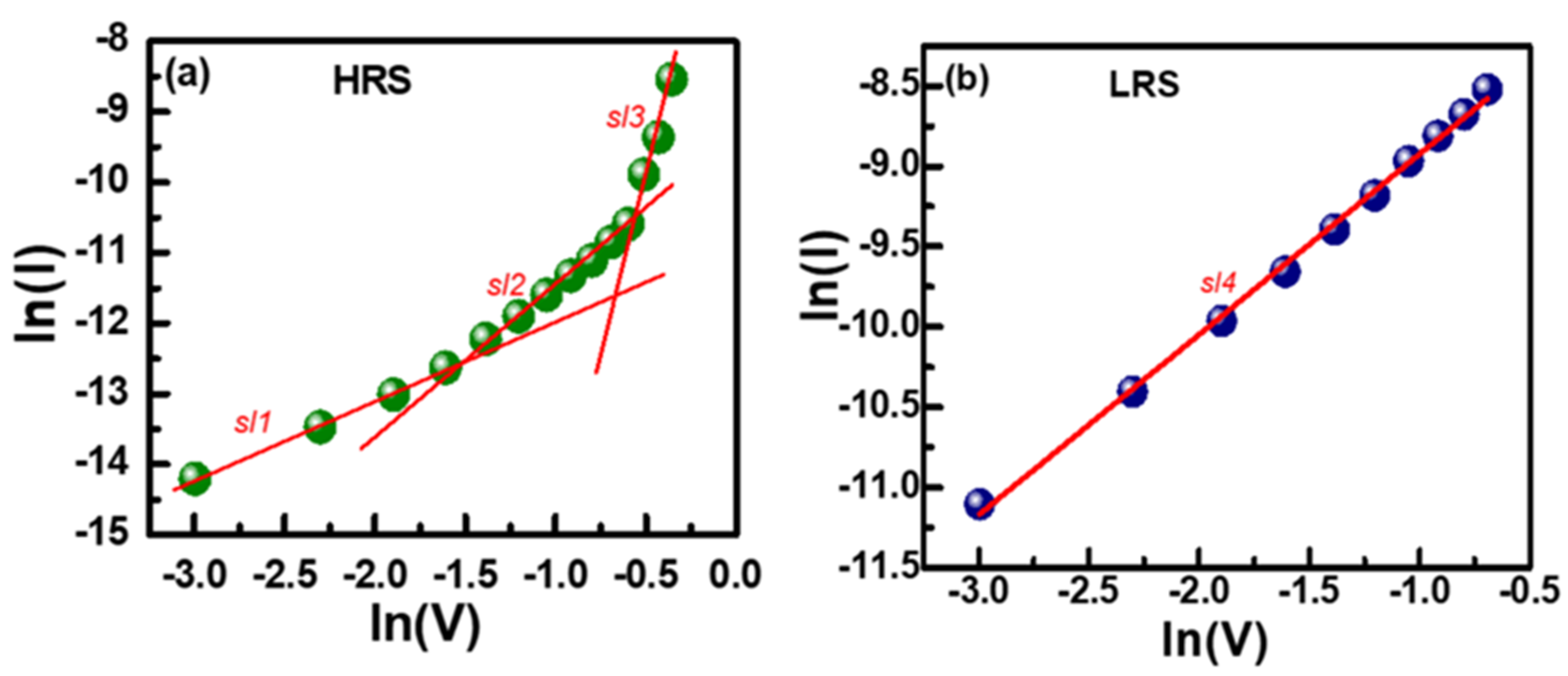
3.1. Diode-Like Threshold Switching Characteristics

The Al/Ag/Al2O3/TiN based S1 device has shown diode-like threshold switching characteristics, as shown in Figure 2. Figure 2a shows consecutive 1000 DC cycles for the via-hole pristine device with a typical area of 4 µm × 4 µm at the low current compliance (CC) of 100 nA following the voltage sweeping path 1→4. Although there is a slight fluctuation of current for 1000 cycles, still an on/off ratio of 10 is being maintained in between path 1 and path 2, as shown in Figure 2b. The device shows high rectifying ratio (RR = IF/IR) (IF = forward bias current = 22.35 nA at Vread = 1.5 V in path 1; IR = reverse bias current = 0.88 pA at Vread = −1 V in path 4) of >2.5 × 10⁴. To evaluate the current conduction mechanism, a typical I-V in Figure 2a has been replotted in log-log scale and fitted linearly. It is observed that the conduction mechanism at low field under both forward (path 1) and reverse (path 4) biases has been dominated by Schottky conduction. This is confirmed from the E1/2 vs. ln (J/T2) plot, as shown in the Figure 2c. The Schottky barrier height (φB) has been calculated using the Equation (1) below [18],
φ B = k T q [ ln ( A ) I ]
where k is the Boltzmann’s constant (1.38 × 10⁻²³ J/K), T is the absolute temperature (300 K), q is the electronic charge (1.6 × 10⁻¹⁹ C), A* is the Richardson’s constant (120 A/cm2-K2), and I is intercept. Schottky emission dominates at electric field range of 50 kV cm−1 to 450 kV cm−1. The obtained intercepts for the forward and reverse biases are −16.02 and −30.09, respectively. The barrier heights from the Equation (1) by using the intercept values are 0.7 eV and 1.11 eV for forward and reverse biases, respectively. However, obtained φB value is lower than the theoretical value of approximately 1.67 eV.
Bai et al. obtained the ΦSB value of 0.58 eV at the Pt/AlOδ interface using Pt/AlOδ/Ta2O5−x/TaOy/Pt structure [19], which is lower than the theoretical φB value of 2.49 eV. Yoon et al. have reported a similar φB value discrepancy at the Pt/Ta2O5 interface (0.7 vs. 2.3 eV) using Pt/Ta2O5/HfO2/TiN structure [20]. They have mentioned that the barrier height lowering is due to the Fermi level pinning near the conduction band edge. According to our previous report [5], the lower φB value of 0.81 eV at the Pt/Al2O3 interface than the theoretical value of 2.57 eV using Pt/Al2O3/MoS2/TaOx/TiN structure is also obtained. This discrepancy is acceptable because of not considering the Fermi level pinning and image charge effects. The switching cycles can be maintained also up to 10,000 cycles, as shown in Figure 2d. However, it can be observed that electrical fatigue during 10,000 cycles led to creation of a non-filamentary path. This in turn has resulted in narrower window as the device is switched to long repeatable cycles. A few Ag+ ions were migrated during switching cycles and some of the Ag atoms were being accumulated inside the Al2O3 SM. Those accumulated Ag atoms were narrowing the switching window. It is expected that this switching could be improved by increasing the negative bias with number of cycles. However, further study is needed in the future. Due to this Ag+ ions migration, the threshold switching is observed, which is explained later.

3.2. Switching Characteristics, Uniformity and Current Conduction

The resistive switching characteristics of the S1 and S2 devices with a typical size of 0.4 µm × 0.4 µm have been investigated. Figure 3a represents the typical forming cycle of pristine S1 and S2 devices. The S1 device required larger forming voltage in comparison to the S2 device due to the presence of thicker Al2O3. (Vform: 3.6 V vs. 1.75 V). After forming step, the devices exhibited bipolar resistive switching characteristics owing to a large amount of Ag+ atoms migrating into the switching layer for a transition to non-volatile memory from diode-like threshold switching. Figure 3b shows the bipolar resistive switching characteristics of the S1 and S2 devices following the voltage sweeping path 1→4. The SET voltages (Vset) of the S1 and S2 devices are found to be 1.5 V and 0.8 V, respectively. The RESET voltages (Vreset) are the same −0.4 V for both the S1 and S2 devices. It is interesting to note that the memory window (ratio of low resistance state (LRS) to high resistance state (HRS)) of the S1 and S2 devices at a read voltage of 0.2 V are approximately 10 and 108, respectively. This is owing to high electric field in S2 devices and remaining Ag in the S1 devices, which is explained below.
Figure 3c shows the Weibull distribution plot of forming voltage for the S1 and S2 devices. We measured 20 randomly chosen devices for every structure with a yield of >85%. In comparison to the S2 devices, the S1 devices require higher forming voltage owing to thicker switching material layer (20 nm vs. 5 nm). Due to the higher thickness of S1 devices, it requires larger electric field to form the initial filament. In the case of S2 devices, increment of electric field across the decreasing thickness is responsible for lower forming voltage, which may also owe to have higher leakage current in the S2 devices. The S1 devices show size dependence forming voltage, while the S2 devices do not show the size dependence forming voltage, which is also due to higher leakage as well as Ag ions are easily migrated through thinner oxide-electrolyte. Here an interesting point to be noted that the S1 device shows better uniformity of forming voltage with compare to the S2 devices. According to our previous report [21], the reason behind this betterment can be attributed to the presence of higher defect density inside the thicker switching layer. The obtained slope values from fitting curve of the Weibull distribution plot following the Equations (2) and (3) support the result [22],
F ( Q ) = 1 e ( Q α 63 % ) β
W ( Q ) = ln [ ln ( 1 F ) ]
where F(Q) is the cumulative distribution function of the failure, Q is the values of measured data, α is the scale factor value from distribution plot at approximately F = 63%, and β is the slope value or shape factor of the fitted curve in Weibull distribution plot. Higher slope values indicate the better uniformity. The obtained slope values are 4.20, 1.73, and 1.60 for the S1, S2 (0.6 µm × 0.6 µm) and S2 (4 µm × 4 µm), respectively. Weibull distribution of the SET voltages for all devices are shown in Figure 3d. In case of larger and smaller sizes, both the S2 devices show good VSet uniformity as compared to the S1 devices. It may possible that the filament length of the S1 devices is longer and filament dissolution length is unstable. However, larger size S2 devices exhibit significantly lower VSet values with compare to smaller size S2 devices due to more number of defects, which might help in easier filament formation/dissolution. From the fitting curve of the distribution plot, the obtained slope values are 1.25, 2.17 and 6.34 for the S1, S2 (0.6 µm × 0.6 µm) and S2 (4 µm × 4 µm) devices. Though the SET voltage uniformity of the smaller size S2 devices has been improved, but still we are lagging from our previously reported result [22]. This uniformity can be further improved by controlling the defects through the annealing process and controlling the Ag+ ion migration by interfacial engineering.
Further, we have explored the current conduction mechanism for the S2 devices. The current transport at HRS is dominating by trap-controlled space-charge-limited-current conduction (TC-SCLC) whereas the current transport at LRS shows Ohmic, as shown in Figure 4. The slope values for current transport fitting curve (ln (I) vs. ln (V)) for HRS are found as sl1 ~ 1.12 (IαV1.1), sl2 ~ 2.04 (IαV2), and sl3 ~ 8.3 (IαV8) from low to high voltage regions, as shown in Figure 4a. Previously, the slope values for HRS are reported as 1.1, 1.3, and 8.5 by Rubi et al. [23] and 1, 2, 4, and 6 by Shang et al. [24]. In case of path 1 (Figure 2a), the slope values are 0.58 and 13.15 at voltage range of 0 to 0.8 V and 1 V to 1.2 V, respectively. This is not the SCLC mechanism. On the other hand, the slope value for ln (I) vs. ln (V) plot for LRS is sl4~1.12 (Figure 4b), which refers to Ohmic behavior. Slightly higher slope value of 1.12 with respect to 1 is attributed to the presence of some defects into the Ag conducting filaments. The switching mechanism is explained later.

3.3. C-V Characteristics and Understanding of Switching

In accordance with the resistive switching, capacitance-voltage (C-V) characteristics of the S2 devices have also been studied, as shown in Figure 5. Typically, 25 mV AC was superimposed on applied DC bias during measurement. Figure 5a–c concurrently exposes the bipolar as well as unipolar capacitive switching nature of the 4 × 4 µm2 size devices. Under the positive bias sweep at a frequency of 1MHz, the concern device switches (in anticlockwise direction following the sweeping path 1→3) from low capacitance state (LCS) to high capacitance state (HCS) at Vset of 4.2 V, as shown in Figure 5a, which is owing to Ag ions migration into the Al2O3 oxide-electrolyte. Next, we have applied the large negative bias from 0 V→−6 V following the sweeping path 4→7 under a frequency of 900 Hz, as shown in Figure 5b. For RESET observation, slightly lower frequency is applied owing to larger stress time. The device first shows a RESET at Vreset of −2.85 V. It is known that there is no option to limit capacitance or compliance current (CC) by using HP4284A LCR meter. Therefore, huge amount of Ag ions are migrated through Al2O3 oxide-electrolyte under positive sweep. It is also not easy to dissolute the Ag filament. In this way, we have observed a faint RESET phenomena at −2.85 V as well as the bipolar switching is observed. By applying more negative bias, it switches to LCS at Vset of −5.05 V, which is owing to regrowth of Ag filament. It is interesting to note that the C-V characteristic observed during −6 V→0 V bias is quite similar to the p-type metal-oxide-semiconductor (MOS) capacitor. Similarly, charge depletion for p-type MOS capacitor also occurs here when we reduce the negative bias. Consequently, as a result of oxide capacitance and depletion layer capacitance being connected in series, measured capacitance decreases with reducing negative bias.
On the other hand, a device swept back to LCS from HCS at the Vreset of 3.1 V and manifests unipolar switch, as shown in Figure 5c, indicated by arrows 4→6. The applied frequency is 900 kHz. By applying negative sweep, the device will be bipolar otherwise it will be unipolar if positive sweep is applied. The Ag ions will be dissolved from the Al2O3 film to Ag electrode. Here, significance of LCS and HCS are corresponding to HRS and LRS of the resistive switching, respectively. In Figure 5a, measured capacitance values for LCS and HCS are found to be 2.6 pF and 1.6 nF, respectively at a Vread of 4 V. Thus, HCS/LCS ratio is high (approximately 600). These results strongly demand that there is a possibility of Ag ion diffusion/trapping through the defects into the Al2O3 oxide-electrolyte. So that diffusion capacitance increases with applied positive bias after the collapse of depletion region. Kamel et al. have reported that metal atoms diffused along oxygen vacancy path in Ag/HfO2/Pt stack and as a result C-V switching occurred [25]. In our previous report, the Cuz+ (z = 1, 2) diffusion in the defects of TaOx film in a Cu/Ti/TaOx/W CBRAM device [26]. If we calculate the geometrical capacitance (C1) of this S2 devices as a parallel plate capacitor according to the following formula:
C 1 = ε 0 k A d
where εo (= 8.854 × 10⁻¹²) is free-space permittivity, k (= 9.1) is dielectric constant of Al2O3 film, ‘A’ is the device area (= 16 µm2), and d (= 5 nm) is the thickness of Al2O3 layer, then the capacitance value of via-hole region is 2.6 × 10⁴ nF. The overlapping area between top and bottom electrode is 36 × 36 µm2. Owing to SiO2 with a thickness of approximately 150 nm, the capacitance is approximately 3 × 10⁴ nF. Total capacitance (C1) including overlapping and via-hole regions is 5.6 × 10⁴ nF. But our measured HCS value (1.6 nF) is approximately 2.9 × 10³ times the geometrical calculated value, C1. This may be Ag ions near Ag electrode or Ag doped Al2O3 oxide-electrolyte, which help to higher k value of Al2O3. In Figure 2a at path 4, the left shift of minimal current is observed. The current of 400–500 fA is obtained at zero bias, which is higher than 100 fA at approximately −0.7 V. This non-zero current at zero bias indicates that this stack has capacity to hold the charges, which may be useful for future nano-battery applications [27].
Figure 5d describes the variation of HCS or ON-state capacitance with different frequencies (f) having ranges from 1 kHz to 1 MHz for both 0.4 × 0.4 and 4 × 4 µm2 sizes of the S1 and S2 devices. Most interesting thing is that irrespective of variation HCS values of all devices are negative in the frequency zone from 1 kHz to 400 kHz. At 400 kHz, the HCS value (−0.67 nF) is almost the same. After that those stacks gain +Ve value of 0.2 nF at 500 kHz and eventually reach to 1.6 nF at 1 MHz with slow expansion. Negative (−Ve) capacitance has been reported by several groups for different structures [25,28,29]. Here, negative capacitance (NC) signifies the inductive nature of the devices. Kamel et al. have also mentioned the inductive nature of Ag/HfO2/Pt device [25]. Misawa et al. have reported also negative capacitance for different structures [30]. Comparatively diffusion of charges is slow process through Al2O3 and corresponding current can’t follow the change of voltages spontaneously. That is why current starts to lag behind the voltage. As a result, phase shift of current with respect to voltage takes place. In lower frequency region (1 kHz to 400 kHz), this phase shift becomes too large and capacitance falls down to negative value. Significantly conductivity increases by leaps and bounds. Thus, the device acts like an inductor in this lower frequency zone. In a true sense, negative capacitance is not like so called static/geometrical capacitance that can store charge. This is only due to phase shift of current in confined low frequency range. This negative capacitance mode can be used to amplify voltage for low power nanoscale devices. Still, it is not totally clear, and further study is needed. In conclusion, this Ag/Al2O3/TiN structure shows very promising for future charge storage applications.

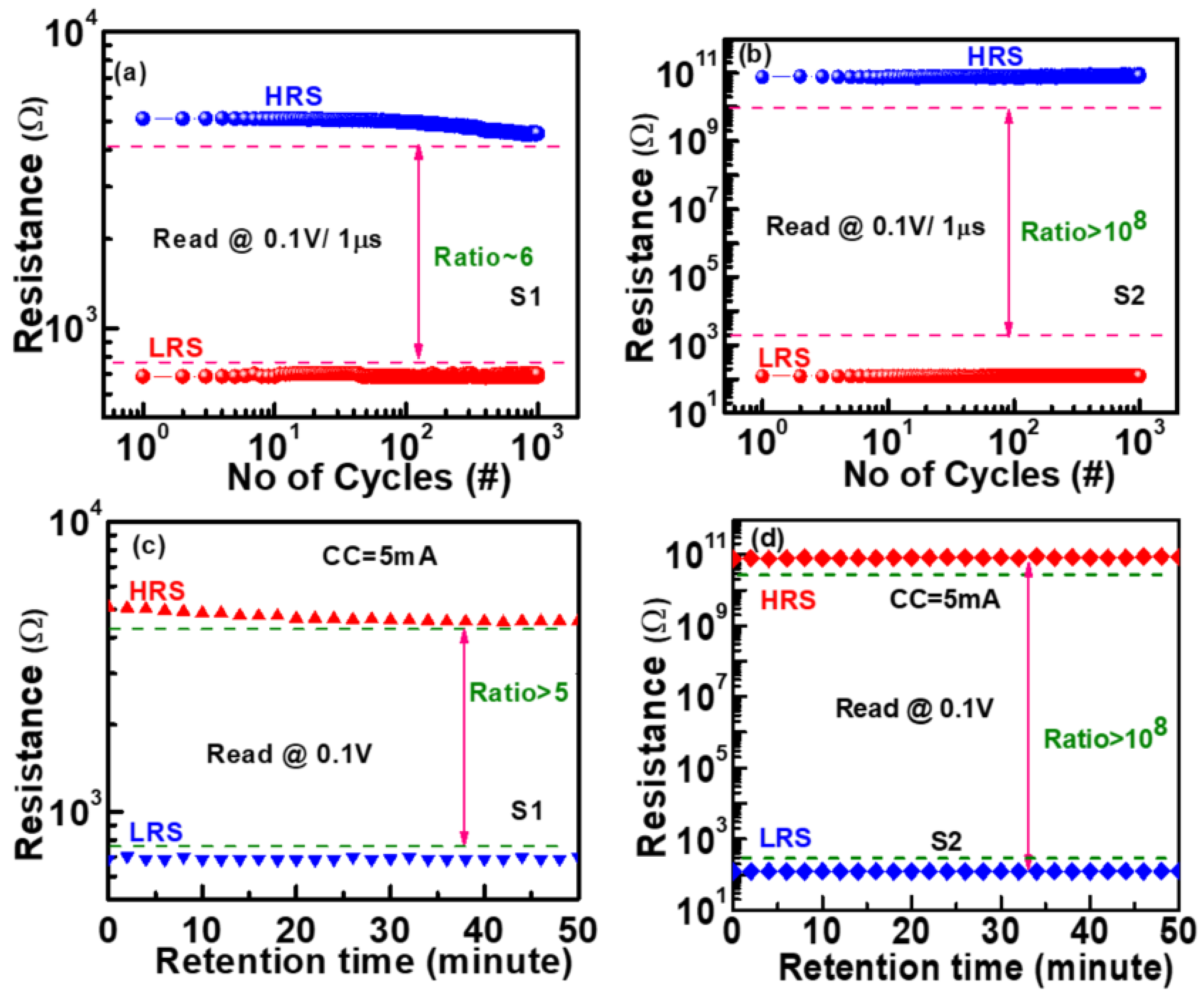
3.4. Read Endurance and Data Retention Characteristics

Read endurance characteristics of the S1 and S2 devices are shown in Figure 6a,b, respectively. After forming, the HRS value of the S1 devices is lower than the pristine one (5 × 10³ Ω vs. 5 × 10¹¹ Ω) owing to remaining Ag into the Al2O3 oxide-electrolyte. It was found that the on/off ratio of the S1 device is only ~6 which is much lower than the S2 devices (>108) at read voltage of 0.1 V using 1μs pulses for 1000 cycles. LRS state of S1 is constant throughout 1000 cycles while HRS state is slightly decreased. This is because as the complete filament is not ruptured, the effective filament height in consecutive cycles for a longer period is slightly decreased, causing lowering of the HRS value after a long period of cycles. However, in the S2 device, both HRS and LRS are the same throughout the measurement. This indicates that the occurrence of complete filament rupture is in the S2 devices.
Typical data retention characteristics of the resistive memory device S1 and S2 at room temperature are shown in Figure 6c,d, respectively at CC of 5 mA where read voltage is 0.1 V. Both S1 and S2 devices show a 50-min data retention. It is clear that the S2 devices possess higher on/off ratio (>108) than S1 (>5) similar as read endurance. This indicates that the S2 devices can retain more data than S1 for a particular period of time and favorable for multilevel switching, which can be studied in future. It is also observed that HRS state for the S1 devices is not uniform and it has a tendency to decrease but the S2 device has uniform LRS and HRS.

3.5. P/E Endurance Characteristics

Figure 7 shows P/E endurance characteristics for the S2 devices under different P/E endurance conditions. P/E endurance is useful as it describes the device reliability under AC pulse, which is also useful for practical implication. The S2 device could undergo few P/E endurance cycles with a huge on/off ratio of >106 with the P/E current of 1 mA/5 mA and 500 µs pulse width as shown in Figure 7a. The extremely high on/off ratio is promising for multilevel switching [31,32] and future neuromorphic computing to ensure the enhance conduction states. Though the device is unable to go for long P/E endurance keeping such a high order on/off ratio, still this result is comparable with recently published works as listed in Table 1 [10,11,33,34,35,36,37,38]. By reducing pulse width from 500 µs to 1 µs, P/E cycles are improved to 100 P/E cycles, as shown in Figure 7b. However, the P/E endurance cycles number has been increased with decreasing of pulse width, but the on/off ratio has been compromised. This is due to the lowering of stress effect by reducing the pulse width.

3.6. CBRAM Mechanism

We have proposed a switching mechanism of Ag/Al2O3/TiN device, as shown in Figure 8. In previous reports using different structures [39,40,41], the metal ions are migrated under external bias and metallic filament is formed. At a CC of >1 mA, the Ag filament formation dissolution has been described. When a positive bias is applied on Ag TE, Ag atoms at Ag/Al2O3 oxidize into Ag ions (Ago→Ag+ + e). Large number of Ag ions start to diffuse into Al2O3 layer. Due to high electric field at TiN BE, these mobile Ag ions migrate towards TiN BE. These Ag ions at TiN BE are deoxidize back to Ag atoms, which results in a formation of conical shaped Ag conducting filament (CF) in between Ag TE and TiN BE. Due to this CF, the device goes to LRS state (Figure 8a). When a negative voltage is applied on Ag TE, the CF start to dissolve at narrow region near TE owing to higher electric field and memory device shifts to HRS (Figure 8b). A neck of a filament can be observed near to the TE. After formation of the pristine devices, a reduction and oxidation at the neck region will be responsible for LRS and HRS of the devices. For the S2 devices, the high electric filed controls across the Al2O3 oxide-electrolyte and high on/off ratio is obtained owing to no remaining Ag atoms into the electrolyte. The process continues for each cycle of applied positive and negative voltage biases. At a low CC of 100 nA for the S1 devices, an Ag nanocrystal-type filament is formed under positive bias on the TE (Figure 8c). By applying negative bias on the TE, almost all Ag atoms will be returned towards the TE and the device will be treated as a pristine one (Figure 8d). This phenomena are similar to the threshold switching because of Ag ions migration through Al2O3 electrolyte with the same polarity [14,15,16,17]. It is possibility that Ag ions could be gathered at the Ag/Al2O3 interface. Therefore, a non-zero current of 400–500 fA is obtained at zero bias in path 4 (Figure 2a). Due to this small amount of Ag atoms, the filament can’t be retained for longer time.

4. Conclusions

In conclusion, diode-like threshold and resistive switching characteristics with current conduction mechanism have been explored using an Al/Ag/Al2O3/TiN structure. Before forming, the thicker Al2O3 layer-based device exhibits diode-like highly uniform threshold switching of >104 cycles with high rectifying ratio of >104, at a low CC of 100 nA. After forming, the 5 nm-thick Al2O3 device shows better uniformity and P/E cycle endurance with high on/off ratio. Negative capacitance at low frequency proves inductive nature and supports unipolar/bipolar resistive switching. Owing to high on/off ratio, the device is capable of multilevel resistive switching and can be potentially used for high-density data storage in near future.

Author Contributions

A.S. wrote the first manuscript and explained data under instruction of S.M. S.R. helped to measure endurance data and modified the manuscript. Y.-F.L. measured resistive switching data under instruction of M.D. and S.M. M.D. measured also the resistive switching characteristics and analyzed data under instruction of S.M. All authors have read and agreed to the published version of the manuscript.

Funding

This work was supported by Ministry of Science and Technology (MOST), Taiwan under contract number: MOST-108-2221-E-182-026.

Acknowledgments

We are thankful to Ministry of Science and Technology (MOST), Taiwan for their financial support under contract number: MOST-108-2221-E-182-026. The authors are grateful to Industrial Technology Research Institute (ITRI), Hsinchu for their support to pattern via-holes.

Conflicts of Interest

The authors hereby declare that they don’t have any interest of competition.

References

  1. Slesazeck, S.; Mikolajick, T. Nanoscale resistive switching memory devices: A review. Nanotechnology 2019, 30, 352003. [Google Scholar] [CrossRef] [PubMed]
  2. Saxena, N.; Persch, C.; Wuttig, M.; Manivannan, A. Exploring ultrafast threshold switching in In3SbTe2 phase change memory devices. Sci. Rep. 2019, 9, 19251. [Google Scholar] [CrossRef] [Green Version]
  3. Baek, E.; Purnama, I.; You, C.Y. Limited stochastic current for energy-optimized switching of spin-Transfer-torque magnetic random-access memory. Phys. Rev. Appl. 2019, 12, 064004. [Google Scholar] [CrossRef]
  4. Lee, T.Y.; Lee, K.; Lim, H.H.; Song, M.S.; Yang, S.M.; Yoo, H.K.; Suh, D.I.; Zhu, Z.W.; Yoon, A.; MacDonald, M.R.; et al. Ferroelectric polarization-switching dynamics and wake-up effect in Si-doped HfO2. ACS Appl. Mater. Interfaces 2019, 11, 3142–3149. [Google Scholar] [CrossRef] [PubMed]
  5. Qiu, J.T.; Samanta, S.; Dutta, M.; Ginnaram, S.; Maikap, S. Controlling resistive switching by using an optimized MoS2 interfacial layer and the role of top electrodes on ascorbic acid sensing in TaOx-based RRAM. Langmuir 2019, 35, 3897–3906. [Google Scholar] [CrossRef] [PubMed]
  6. Dutta, M.; Maikap, S.; Qiu, J.T. Controlling conductive filament and tributyrin sensing using an optimized porous iridium interfacial layer in Cu/Ir/TiNxOy/TiN. Adv. Electron. Mater. 2019, 5, 1800288. [Google Scholar]
  7. Lanza, M.; Wong, H.S.P.; Pop, E.; Ielmini, D.; Strukov, D.; Regan, B.C.; Larcher, L.; Villena, M.A.; Yang, J.J.; Goux, L.; et al. Recommended methods to study resistive switching devices. Adv. Electron. Mater. 2018, 4, 1800143. [Google Scholar] [CrossRef] [Green Version]
  8. Jana, D.; Roy, S.; Panja, R.; Dutta, M.; Rahaman, S.Z.; Mahapatra, R.; Maikap, S. Conductive-bridging random access memory: Challenges and opportunity for 3D architecture. Nanoscale Res. Lett. 2015, 10, 188. [Google Scholar] [CrossRef] [Green Version]
  9. Belmonte, A.; Radhakrishnan, J.; Goux, L.; Donadio, G.L.; Kumbhare, P.; Redolfi, A.; Delhougne, R.; Nyns, L.; Devulder, W.; Witters, T.; et al. Co active electrode enhance CBRAM and scaling potential. In Proceedings of the IEEE International Electron Devices Meeting 2019, San Francisco, CA, USA, 7–11 December 2019. [Google Scholar]
  10. Woo, H.; Vishwanath, S.K.; Jeon, S. Excellent resistive switching performance of Cu−Se-based atomic switch using lanthanide metal nanolayer at the Cu−Se/Al2O3 interface. ACS Appl. Mater. Interfaces 2018, 10, 8124–8131. [Google Scholar] [CrossRef]
  11. Kim, S.M.; Kim, H.J.; Jung, H.J.; Kim, S.H.; Park, J.Y.; Seok, T.J.; Park, T.J.; Lee, S.W. Highly uniform resistive switching performances using two-dimensional electron gas at a thin-film heterostructure for conductive bridge random access memory. ACS Appl. Mater. Interfaces 2019, 11, 30028–30036. [Google Scholar]
  12. Sleiman, A.; Sayers, P.W.; Mabrook, M.F. Mechanism of resistive switching in Cu/AlOx/W nonvolatile memory structures. J. Appl. Phys. 2013, 113, 164506. [Google Scholar] [CrossRef]
  13. Belmonte, A.; Kim, W.; Chan, B.T.; Heylen, N.; Fantini, A.; Houssa, M.; Jurczak, M.; Goux, L. 90 nm W\Al2O3\TiW\Cu 1T1R CBRAM cell showing low-power, fast and disturb-free operation. In Proceedings of the 5th IEEE International Memory Workshop, Monterey, CA, USA, 26–29 May 2013. [Google Scholar]
  14. Wang, Z.; Rao, M.; Midya, R.; Joshi, S.; Jiang, H.; Lin, P.; Song, W.; Asapu, S.; Zhuo, Y.; Li, C.; et al. Threshold switching of Ag or Cu in dielectrics: Materials, mechanism, and applications. Adv. Funct. Mater. 2018, 28, 1704862. [Google Scholar] [CrossRef]
  15. Wang, Z.; Joshi, S.; Savel’ev, S.E.; Jiang, H.; Midya, R.; Lin, P.; Hu, M.; Ge, N.; Strachan, J.P.; Li, Z.; et al. Memristors with diffusive dynamics as synaptic emulators for neuromorphic computing. Nat. Mater. 2017, 16, 101–108. [Google Scholar] [CrossRef] [Green Version]
  16. Lee, D.; Kwak, M.; Moon, K.; Choi, W.; Park, J.; Yoo, J.; Song, J.; Lim, S.; Sung, C.; Banerjee, W.; et al. Various threshold switching devices for integrate and fire neuron applications. Adv. Electron. Mater. 2019, 5, 1800866. [Google Scholar] [CrossRef]
  17. Samanta, S.; Han, K.; Das, S.; Gong, X. Improvement in threshold switching performance using Al₂O₃ interfacial layer in Ag/Al₂O₃/SiOx/W cross-point platform. IEEE Electron Device Lett. 2020, 41, 924–927. [Google Scholar] [CrossRef]
  18. Roy, A.; Maikap, S.; Tzeng, P.-J.; Qiu, J.T. Sensing characteristics of dopamine using Pt/n-Si structure. Vacuum 2020, 172, 109050. [Google Scholar] [CrossRef]
  19. Bai, Y.; Wu, H.; Wu, R.; Zhang, Y.; Deng, N.; Yu, Z.; Qian, H. Study of multi-level characteristics for 3D vertical resistive switching memory. Sci. Rep. 2014, 4, 5780. [Google Scholar] [CrossRef] [PubMed] [Green Version]
  20. Yoon, J.H.; Song, S.J.; Yoo, I.H.; Seok, J.Y.; Yoon, K.J.; Kwon, D.E.; Park, T.H.; Hwang, C.S. Highly uniform, electroforming free, and self-rectifying resistive memory in the Pt/Ta2O5/HfO2/TiN structure. Adv. Funct. Mater. 2014, 24, 5086–5095. [Google Scholar] [CrossRef]
  21. Panja, R.; Roy, S.; Jana, D.; Maikap, S. Impact of device size and thickness of Al2O3 film on the Cu pillar and resistive switching characteristics for 3D cross-point memory application. Nanoscale Res. Lett. 2014, 9, 692. [Google Scholar] [CrossRef] [Green Version]
  22. Jana, D.; Samanta, S.; Roy, S.; Lin, Y.F.; Maikap, S. Observation of resistive switching memory by reducing device size in a new Cr/CrOx/TiOx/TiN structure. Nano–Micro Lett. 2015, 7, 392–399. [Google Scholar] [CrossRef] [Green Version]
  23. Rubi, D.; Tesler, F.; Alposta, I.; Kalstein, A.; Ghenzi, N.; Marlasca, F.G.; Rozenberg, M.; Levy, P. Two resistive switching regimes in thin film manganite memory devices on silicon. Appl. Phys. Lett. 2013, 103, 163506. [Google Scholar] [CrossRef] [Green Version]
  24. Sheng, S.D.; Wang, Q.; Chen, D.L.; Dong, R.; Li, X.M.; Zhang, W.Q. Effect of carrier trapping on the hysteretic current-voltage characteristics in Ag/La0.7Ca0.3MnO3/Pt heterostructures. Phys. Rev. B 2006, 73, 245427. [Google Scholar] [CrossRef]
  25. Kamel, F.E.; Gonon, P.; Jomni, F.; Yangui, B. Observation of negative capacitances in metal-insulator-metal devices based on a-BaTiO3: H. Appl. Phys. Lett. 2008, 93, 042904. [Google Scholar] [CrossRef]
  26. Rahaman, S.Z.; Maikap, S.; Tien, T.C.; Lee, H.Y.; Chen, W.S.; Chen, F.T.; Kao, M.J.; Tsai, M.J. Excellent resistive memory characteristics and switching mechanism using a Ti Nanolayer at the Cu/TaOx interface. Nanoscale Res. Lett. 2012, 7, 345. [Google Scholar] [CrossRef] [PubMed] [Green Version]
  27. Valov, I.; Linn, E.; Tappertzhofen, S.; Schmelzer, S.; Hurk, J.V.D.; Lentz, F.; Walser, R. Nanobatteries in redox-based resistive switches require extension of memristor theory. Nat. Commun. 2013, 4, 1771. [Google Scholar] [CrossRef] [PubMed] [Green Version]
  28. Ershov, E.; Liu, H.C.; Li, L.; Buchanan, M.; Wasilewski, Z.R.; Jonscher, A.K. Negative capacitance effect in semiconductor devices. IEEE Trans. Electron Devices 1998, 45, 2196–2206. [Google Scholar] [CrossRef] [Green Version]
  29. Khan, A.I.; Chatterjee, K.; Wang, B.; Drapcho, S.; You, L.; Serrao, C.; Bakaul, S.R.; Ramesh, R.; Salahuddin, S. Negative capacitance in a ferroelectric capacitor. Nat. Mater. 2015, 14, 182–186. [Google Scholar] [CrossRef] [PubMed]
  30. Misawa, T. Impedance of bulk semiconductor in junction diode. J. Phys. Soc. Jpn. 1957, 12, 882–890. [Google Scholar] [CrossRef]
  31. Gogurla, N.; Mondal, S.P.; Sinha, A.K.; Katiyar, A.K.; Banerjee, W.; Kundu, S.C.; Ray, S.K. Transparent and flexible resistive switching memory devices with a very high on/off ratio using gold nanoparticles embedded in a silk protein matrix. Nanotechnology 2013, 24, 345202. [Google Scholar] [CrossRef]
  32. Attarimashalkoubeh, B.; Prakash, A.; Lee, S.; Song, J.; Woo, J.; Misha, S.H.; Tamanna, N.; Hwang, H. Effects of Ti buffer layer on retention and electrical characteristics of Cu-based conductive-bridge random access memory (CBRAM). ECS Solid State Lett. 2014, 3, 120–122. [Google Scholar] [CrossRef] [Green Version]
  33. Ju, J.H.; Jang, S.K.; Son, H.; Park, J.H.; Lee, S. High performance bi-layer atomic switching devices. Nanoscale 2017, 9, 8373–8379. [Google Scholar] [CrossRef]
  34. Wang, Y.; Liu, Q.; Long, S.; Wang, W.; Wang, Q.; Zhang, M.; Zhang, S.; Li, Y.; Zuo, Q.; Yang, J.; et al. Investigation of resistive switching in Cu-doped HfO2 thin film for multilevel non-volatile memory applications. Nanotechnology 2010, 21, 045202. [Google Scholar] [CrossRef] [PubMed]
  35. Cao, X.; Han, Y.; Zhou, J.; Zuo, W.; Gao, X.; Han, L.; Pang, X.; Zhang, L.; Liu, Y.; Cao, S. Enhanced switching ratio and long-term stability of flexible RRAM by anchoring polyvinyl ammonium on perovskite grains. ACS Appl. Mater. Interfaces 2019, 11, 35914–35923. [Google Scholar] [CrossRef]
  36. Kang, D.H.; Choi, W.Y.; Woo, H.; Jang, S.; Park, H.Y.; Shim, J.; Choi, J.W.; Kim, S.; Jeon, S.; Lee, S.; et al. Poly-4-vinylphenol (PVP) and Poly(melamine-co-formaldehyde) (PMF)-based atomic switching device and its application to logic gate circuits with low operating voltage. ACS Appl. Mater. Interfaces 2017, 9, 27073–27082. [Google Scholar] [CrossRef] [PubMed]
  37. Park, J.H.; Kim, S.H.; Kim, S.G.; Heo, K.; Yu, H.Y. Nitrogen-induced filament confinement technique for a highly reliable hafnium-based electrochemical metallization threshold switch and its application to flexible logic circuits. ACS Appl. Mater. Interfaces 2019, 11, 9182–9189. [Google Scholar] [CrossRef] [PubMed]
  38. Zhao, X.; Liu, S.; Niu, J.; Liao, L.; Liu, Q.; Xiao, X.; Lv, H.; Long, S.; Banerjee, W.; Li, W.; et al. Confining cation injection to enhance CBRAM performance by nanopore graphene layer. Small 2017, 13, 1603948. [Google Scholar] [CrossRef]
  39. Roy, S.; Maikap, S.; Sreekanth, G.; Dutta, M.; Jana, D.; Chen, Y.Y.; Yang, J.R. Improved resistive switching phenomena and mechanism using Cu-Al alloy in a new Cu:AlOx/TaOx/TiN structure. J. Alloy. Compd. 2015, 637, 517–523. [Google Scholar] [CrossRef]
  40. Chang, T.-C.; Chang, K.-C.; Tsai, T.-M.; Chu, T.-J.; Sze, S.M. Resistance random access memory. Mater. Today 2016, 19, 254–264. [Google Scholar] [CrossRef]
  41. Ginnaram, S.; Qiu, J.T.; Maikap, S. Role of the Hf/Si interfacial layer on the high performance of MoS2-based conductive bridge RAM for artificial synapse application. IEEE Electron Device Lett. 2020, 41, 709–712. [Google Scholar] [CrossRef]
Figure 1. HRTEM (high-resolution transmission electron microscopy) image of the TE/Al2O3/BE structure.
Electronics 09 01106 g001
Figure 2. (a) Consecutive 1000 switching cycles of the S1 devices at low CC of 100 nA. (b) Current vs. no. of cycles plot of path 1 and path 2 at Vread of 0.6 V. (c) Schottky fitting for path 1 and path 4 at low field region in the forward and reverse biases. (d) RepeaTable 10,000 I-V cycles of the S1 device.
Electronics 09 01106 g002
Figure 3. (a) Typical forming cycle of the pristine S1 and S2 devices and (b) I-V switching characteristics of the S1 and S2 devices under CC of 5 mA. Weibull distribution plots of the S1 and S2 devices to study the (c) device-to-device forming voltage and (d) SET voltage variations by using linear fitting.
Electronics 09 01106 g003
Figure 4. I-V fitting characteristics (a) on HRS current are shown. This shows SCLC (space-charge-limited-current) conduction through the dissolution gap of the filaments. (b) Ohmic nature obtained from the fitting of current-voltage characteristics at LRS current.
Electronics 09 01106 g004
Figure 5. C-V characteristics by applying (a) positive sweep voltage of 4 V and (b) negative sweep voltage of −6 V for the S2 devices. The device size is 4 × 4 µm2. (c) Interpretation of unipolar switching by C-V characteristics. (d) Frequency dependent C-V response of the S1 (20 nm) and S2 (5 nm) devices with sizes of 0.4 × 0.4 µm2 and 4 × 4 µm2.
Electronics 09 01106 g005
Figure 6. Read endurance characteristic of the (a) S1 and (b) S2 devices at read voltage of 0.1 V using 1 µs pulse width. Data retention characteristics of the (c) S1 and (d) S2 at CC of 5 mA using read voltage of 0.1 V.
Electronics 09 01106 g006
Figure 7. Typical P/E endurance characteristic of the S2 devices using (a) 500 µs and (b) 1 µs pulse width.
Electronics 09 01106 g007
Figure 8. Schematic views of conducting filament growth and dissolution mechanism at different current compliances: (a) set at a CC of 1 mA, (b) reset after set at 1 mA, (c) set at a CC of 100 nA, and (d) reset after set at 100 nA.
Electronics 09 01106 g008
Table 1. Device performance comparison based on high on/off ratio with recently published results in literature.
Device StructureP/E Voltage (V)P/E Current (mA)P/E Pulse Width (µs)Cycle No.On/Off RatioRetention (s)
Al/Ag/Al2O3/TiN (This work) 1.5/−1.21/5500/50010>1063 × 103
Cu-Se/Nd/Al2O3/Pt [10]1.5/−20.1/0.1500/50010,000105104 at 85 °C
Cu/Ti/Al2O3/TiO2 [11] 7/−90.1/105/5107105106
Cu/TaOx/Ta2O5-x/Pt [33]-/-0.1/0.1-3000~105>104 at 85 °C
Cu/HfO2:Cu/Pt [34] -/-1/10.01/100>100107105
Al/CH3NH3Pbl3:PVAm.Hl/ITO/Glass [35] 3/−1100/100104/104500>105104
Cu/Ti/PVP-PMF/Pt [36]1/−0.51/5104/104>103>103>103at 85 °C
Ag/HfOx:N/Pt [37] 2/-0.1/-50/501065 × 108-
Cu/NG/HfO2 [38] 4/−40.5/0.50.5/0.5107>1062 × 105 at 125 °C

