Article

A Design of Low-Power 10-bit 1-MS/s Asynchronous SAR ADC for DSRC Application

College of Information and Communication Engineering, Sungkyunkwan University, Seoul 16419, Korea
*
Author to whom correspondence should be addressed.
Electronics 2020, 9(7), 1100; https://doi.org/10.3390/electronics9071100
Submission received: 17 June 2020 / Revised: 30 June 2020 / Accepted: 1 July 2020 / Published: 6 July 2020
(This article belongs to the Special Issue Analog/Digital Mixed Circuit and RF Transceiver Design)

Abstract

:
A design of low-power 10-bit 1 MS/s asynchronous successive approximation register analog-to-digital converter (SAR ADC) is presented in this paper. To improve the linearity of the digital-to-analog converter (DAC) and energy efficiency, a common mode-based monotonic charge recovery (CMMC) switching technique is proposed. The proposed switching technique consumes only 63.75 CVREF2 switching energy, which is far less as compared to the conventional switching technique without dividing or adding additional switches. In addition, bootstrap switching is implemented to ensure enhanced linearity. To reduce the power consumption from the comparator, a dynamic latch comparator with a self-comparator clock generation circuit is implemented. The proposed prototype of the SAR ADC is implemented in a 55 nm CMOS (complementary metal-oxide-semiconductor) process. The proposed architecture achieves a figure of merit (FOM) of 17.4 fJ/conversion, signal-to-noise distortion ratio (SNDR) of 60.39 dB, and an effective number of bits (ENOB) of 9.74 bits with a sampling rate of 1 MS/s at measurement levels. The implemented SAR ADC consumes 14.8 µW power at 1 V power supply.

1. Introduction

Dedicated Short Range Communication (DSRC) is one of the widely used wireless communication technologies for communication systems in automotive vehicles. The communication systems, like vehicle systems, intelligent transportation systems (ITS), and electronic toll collection systems (ETCS), make use of DSRC channels to carry out short-range exchange of information among the devices, such as on-board units (OBUs), road-side units (RSUs), or handheld devices carried by pedestrians [1,2]. It has the ability to provide a reliable and efficient vehicle-to-vehicle (V2V), vehicle-to-infrastructure (V2I), and vehicle-to-device (V2X) communications to support safety, mobility, and environmental applications. An OBU generally requires low power, good reliability, long battery life, and low cost. To meet these requirements, a fully-integrated on-chip design of a transceiver and a baseband is the best option.
Figure 1 depicts the top block diagram of the DSRC receiver system, which consists of a low-noise amplifier (LNA), a mixer (MIXER), a band-pass filter (BPF), a received signal strength indicator (RSSI) circuit with a 10-bit ADC, and a programmable gain amplifier (PGA). The BPF is inserted between the PGA and MIXER so that the spur and out-of-band noise, such as the DC offset at low frequency and flicker noise before the in-band is passed into the PGA, and the adjacent-channel signals at high frequency can be removed [3,4,5]. According to the detected signal strength, it is important to maintain the gain of each block in the receiver to maintain an appropriate signal level into the ADC. In the proposed architecture, an RSSI with a low power 10-bit ADC block is embedded in the receiver. The RSSI assessed the received input signal strength from the antenna and then the 10-bit ADC digitized it. The digitized data of the ADC goes to the baseband. An on-chip low power ADC is required along with the RSSI for a wider input range and low power consumption with faster settling.
Successive approximation register (SAR) ADC architecture has been a very popular architecture for many applications, as it features the CMOS downscale size [6,7,8]. SAR ADC does not require any amplifier, as it requires high power consumption to achieve the required performance as compared to the other ADC structures, such as sigma-delta (SD ADC). The unique low power and medium resolution characteristics of the SAR ADC also makes it an attractive option. For medium-resolution ADCs, the SAR ADC approach provides better power efficiency [9]. An ADC with on-chip input single-independent calibration is presented in [10,11]. In [10] the drawback of conventional split-capacitor calibration can be overcome with the proposed calibration by maintaining fast convergence. In [11], to reduce the switching energy a split-capacitor array with a dual thermometer decoder is presented for multi-channel neural recording.
A SAR ADC can be implemented in either fully differential [12] or in a single-ended [13] topology. Although the fully-differential topology has its advantages, namely, better common-mode noise rejection, better distortion performance, and increased output voltage swing, it is not always favored in terms of area and power constraints. Firstly, the fully-differential ADCs require extra design efforts and power, e.g., for the common-mode feedback and dedicated circuit to generate the explicit voltage. Secondly, the fully-differential SAR ADC usually consumes a larger area for the capacitor array. Although the calculated size of the unit capacitor in fully-differential designs could be almost halved, the layout size of the dual capacitor array is usually larger, mainly because the dummy structures inside do not scale well with the size of the unit capacitor. Several methods have been proposed to reduce the size of conventional fully-differential capacitor array [14,15] without applying digital calibration techniques; however, there are drawbacks. In [14], the size of capacitor array is halved by using top-plate sampling technique. This results in input dependent common-mode for the comparator and potential non-linearity error. In [15], the bottom-plate sampling technique is preserved while reducing the capacitor array size to its half. The adopted technique could potentially forward bias junction diodes and cause nonlinearity errors. Although recent publications for different applications mainly focus on the fully differential topology, we chose to design a single-ended SAR ADC due to the power and area constraints for the RSSI application. The degraded common-mode noise rejection ratio can be compensated at the system level together with a single-ended analog front-end with high common mode rejection ratio (CMRR). To increase the power efficiency of the SAR ADC, reducing the switching energy from the CDAC is very important. Recently there have been many studies in the switching scheme for CDACs to improve the energy efficiency. Among the various tri-level switching schemes [16,17,18,19,20,21,22], the best switching efficiency achieves a 98.8% reduction in the switching energy as compared to a conventional SAR switching. A bootstrap sampling switch is implemented to improve the linearity, and a non-binary redundant algorithm and rail-to-rail comparator is presented to improve the performance of the differential ADC, but the architecture of the rail-to-rail comparator requires greater power consumption [23].
The proposed work focuses on a single-ended ADC architecture to be used along with RSSI, in which multiple techniques have been implemented to optimize the area and power efficiency as follows:
  • A common mode-based monotonic charge recovery (CMMC) technique for switching is proposed to optimize the switching energy of capacitive DAC. The proposed technique of the SAR ADC employs a common mode based monotonic charge recovery switching scheme, which has the advantage of the regular VCM based switching scheme, resulting in reduction of the switching energy.
  • A self-comparator clock generator circuit controlled by asynchronous SAR logic is implemented with a modified dynamic latch comparator to eliminate the necessity of an external clock and power optimization of the comparator.
The key idea of the proposed paper is to reduce the power consumption and optimize the SAR ADC speed. The proposed CMMC technique consumes less switching energy as compared to the conventional switching architecture.
In Section 2, we have discussed the proposed architecture of asynchronous SAR ADC and its timing diagram. Section 3 describes the sub-blocks of the ADC, including bootstrap switching, the proposed architecture of the capacitive DAC with a CMMC switching technique, and a dynamic latch comparator with self-comparator clock generation circuitry. Section 4 discusses the measurement results of the proposed ADC structure and, finally, the conclusion is presented in Section 5.

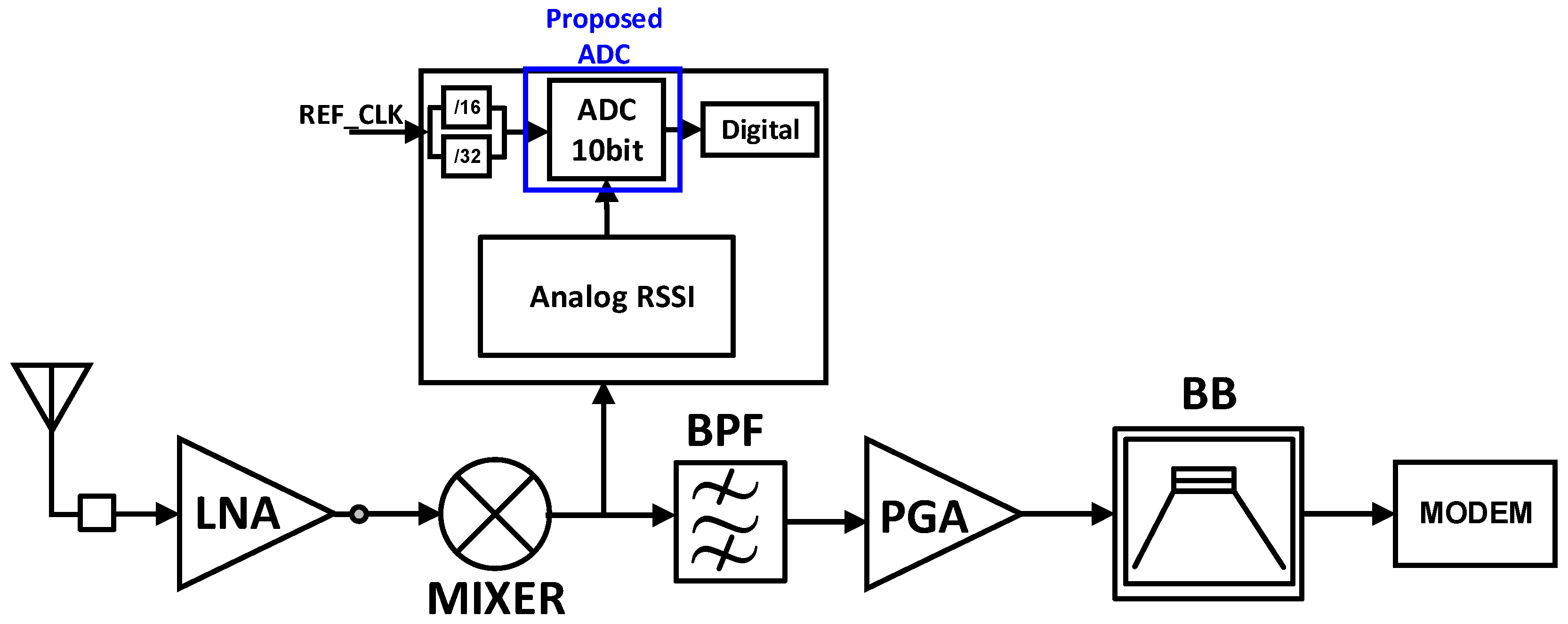
2. The Proposed ADC Architecture

The proposed architecture of 10-bit 1-MS/s SAR ADC consists of a bootstrap switch, a capacitive DAC, a dynamic latched comparator with self-comparator clock generation circuit, and asynchronous SAR logic, as shown in Figure 2. The timing diagram of the proposed architecture is illustrated in Figure 3. A conventional asynchronous SAR has a fixed time delay for each bit settling which may result in waste of time during this process.
On the other hand, this extra time can be utilized as the MSB bit with higher capacitance needs a longer settling time as compared to the LSB bit with comparatively very low capacitance. In the proposed design, the self-comparator clock generator circuit ensures the optimization of the settling time for MSB bits and LSB bits. An energy efficient common mode-based monotonic charge recovery (CMMC) switching technique is presented to decrease the switching energy from CDAC. The CMMC switching technique reduces the parasitic capacitance effect from the capacitive DAC and improves the linearity. For the 10-bit case, 63.75 CVREF2 switching energy is consumed by the proposed CMMC switching technique.

3. Circuit Implementation

3.1. Bootstrap Switching

The on-resistance of the sampling switch must be signal independent, to ensure high linearity. Overdrive voltage depends upon the VIN for NMOS switches, and constant overdrive voltage is achieved through bootstrap switching. The implemented boostrap switching schematic is shown in Figure 4. When CLKSAM is low in the hold phase, capacitor C1 is charged to VDD with M1 and M4. When CLKSAM is high in the tracking phase, the input voltage VIN is connected to the bottom plate VB through M8, and the boosted voltage VT is connected to the gate of sampling switch M9 through M3. Transistor M6 is initially used to turn on M3. Since M6 is turned off if VIN is higher than VDD—Vth,n, Transistor M7 is included to ensure that M3 stays on while VB is charged to VIN. When CLKSAM goes low, M3 is turned off with M5, and Vg is discharged through M2 and NMOS of the inverter. Transistor M2 protects the inverter MOSFETs from the boosted voltage Vg during the tracking phase.

3.2. CDAC

The proposed CMMC switching for SAR ADC is presented in Figure 5. During the sampling mode, the bottom plate of the capacitors in CDAC is connected to VCM while the top plate is connected to the input signal, VIN. After sampling, without consuming any energy from the capacitor array, the first signed bit can be immediately determined. The next bit cycle either charges the capacitor from VCM to VREFT or discharges the capacitor from VCM to VREFB, depending upon the first comparison bit value.
The proposed CMMC switching architecture requires 2n−1 capacitors for the n-bit ADC, while a conventional ADC requires 2n capacitors [24], which is half of the conventional ADCs.
CMMC switching does not require the most significant bit (MSB) capacitor. There are few differences and similarities between the proposed CMMC switching and monotonic switching. Both switching schemes require half of the total capacitance, as these switching schemes have one more bit resolution than other switching schemes. The voltage either moves by the full VREF, towards the top or bottom half of the CDAC, in the monotonic switching.
On the contrary, the proposed CMMC switching algorithm moves the voltage by VREF − VCM = (1/2)VCM on both the top and bottom half of the DAC. The energy consumption is proportional to CV2 and the energy consumption of the monotonic switching is proportional to CVREF2, hence, the energy consumption of the proposed CMMC switching is proportional to 2C(VREF/2)2 = (1/2)CVREF2. As we can conclude that, the proposed CMMC switching algorithm is more energy efficient as compared to the monotonic switching algorithm. The common-mode voltage VCM of the DAC in the proposed CMMC switching algorithm does not change as compared to the monotonic switching algorithm, this improves the static performance of the ADC and it simplifies the designing of the comparator for ADC. The switching energy of the proposed switching architecture in each stage is represented in Figure 5. The CMMC switching algorithm consumes far less energy as compared to the conventional implementation. For 10-bit case, 63.75 CVREF2 switching energy is consumed by the proposed CMMC switching technique. The fast Fourier transform (FFT) spectrum of the behavioral simulation is done in MATLAB® for the proposed switching architecture with 1% unit capacitor mismatch as shown in Figure 6. The static performance integral non-linearity (INL) and differential non-linearity (DNL) of the proposed switching with 1% unit capacitor mismatch, as shown in Figure 7.

3.3. Dynamic Latch Comparator

The comparator is a critical building block for a SAR ADC, because the noise of comparator dominates the ADC performance [25,26]. Figure 8 shows the schematic of implemented dynamic latch comparator. The schematic of self-comparator clock (CCLK) generation circuit is depicted in Figure 9. The operation of the comparator and CCLK generation is explained below.
In Figure 9, when CLK is high, NMOS M6 turns on which results in resetting the comparator clock CCLK to low. It makes both of the comparator outputs OUTP and OUTN reset to high, which turn off PMOS M9 and M11, respectively. In the meantime, node A discharges to low through NMOS M10 and node B charges to high through PMOS M16. On low CLK, the conversion process starts, which switches on the PMOS M5 and M7 and switches off the NMOS M6 and M8. As a result, on high CCLK the comparator will be activated. The PMOS M9 or M11 will be turned on and node A goes to high, when comparison decision is made. On low CCLK, M8 is turned on. The output of AND gate will be transferred to the gate of NMOS M17 through transmission switch TG1 or TG2. It will turn-on the NMOS M17 as both inputs of AND gate A and B are high. As a result node B will be discharged to low and turns on the NMOS M13, which will again push node A to low. Consequently, the next rising edge of CCLK appears when PMOS M7 is turned-on.
The asynchronous SAR logic adjusts the comparison cycle of different bits by generating the control signals for TG1 and TG2. The DAC settling time, comparison time and the logic delay constitutes one comparison cycle. As MSB has larger capacitance, so it usually requires longer time for its settling. To overcome this issue, comparatively longer comparison periods are ensured for higher four MSBs by switching on TG2 for the first four comparison cycles. The comparison time for the remaining LSB bits is set by switching on TG1. The on resistance of each LSB is tuned to ensure the same settling time for all LSB bits. On completion of all of the comparisons in one conversion process, the latch dynamic comparator is turned off by the EN signal from the asynchronous SAR logic, hence resulting in low power consumption.

4. Measurement Results

The proposed architecture is implemented and tested with 55 nm CMOS technology. A die photograph of the proposed ADC architecture is shown in Figure 10. The implemented ADC operates at under 1 V supply power. The measured FFT spectrum of the ADC with different input frequencies at a sampling rate of 1 MS/s is shown in Figure 11. The proposed architecture achieves the ENOB of 9.74 bits and SNDR of 60.39 dB at input frequency of 250.97 kHz, as shown in Figure 11a, and with an input frequency of 450.19 kHz it achieves the ENOB of 9.59 bits and SNDR of 59.49 dB at a sampling speed of 1 MS/s which is shown in Figure 11b.
Figure 12 shows the INL and DNL results to represents the linearity performance of the ADC. The measured INL and DNL values of the proposed architecture are −0.7/0.6 and −0.5/0.7, respectively. Figure 13 shows the overall power breakdown of the proposed single-ended asynchronous SAR ADC which includes the CDAC, bootstrap switch, SAR logic, comparator, and asynchronous clock generator.
Table 1 summarizes the comparison of the proposed architecture with other state-of-the art SAR ADCs and shows their measured performance. The power efficiency can be evaluated by the Figure of Merit (FOM), which can be calculated as depicted in Equation (1).
FOM = Power min { F S , 2 × ERBW } 2 ENOB
where sampling frequency is represented by FS, power consumption of the ADC is presented as power, and the effective resolution bandwidth is represented by ERBW. The proposed ADC achieves a FOM of 17.3 fJ/step. Table 1 shows the comparison with other state-of-the-art SAR ADCs and summarizes the performance of the proposed asynchronous SAR ADC.

5. Conclusions

This paper presented a low-power 10-bit asynchronous SAR ADC operating at a speed of 1-MS/s. A CMMC technique is proposed to decrease the switching energy from the CDAC. By decreasing the parasitic capacitance effect, static performance of the ADC is improved in the proposed switching technique. The common-mode voltage of proposed CMMC technique has been unchanged, which makes the designing of comparator easy. The proposed CMMC switching technique consumes 63.75 CVREF2 energy for 10-bit operation. Additionally, a dynamic latch comparator with self-comparator clock generating circuit has been implemented to carry out the power optimized operation and good resolution. Comparator clock generator circuit is controlled by asynchronous SAR logic to adjust the settling time of the MSB and LSB bits. The proposed prototype of the SAR ADC is realized in 55 nm CMOS technology. The proposed architecture achieves a FOM of 17.3 fJ/conv-step with the ENOB of 9.74 bits and SNDR of 60.39 dB at measurement level when operating at 1 MS/s with a 1 V supply.

Author Contributions

Conceptualization: D.V. and K.S.; methodology: D.V.; software: D.V., K.S., and S.J.K.; validation: D.V. and K.S.; formal analysis: D.V. and K.S.; investigation: D.V. and K.S.; resources: D.V.; data curation: D.V. and K.S.; writing—original draft preparation: D.V. and K.-Y.L.; writing—review and editing: D.V., D.K., Y.G.P., S.-S.Y., and K.-Y.L.; visualization: D.V., K.S., D.K., and K.-Y.L.; supervision: K.C.H., Y.Y., and K.-Y.L.; project administration: K.-Y.L. All authors have read and agreed to the published version of the manuscript.

Funding

This research received no external funding.

Acknowledgments

This research was supported by the MOTIE (Ministry of Trade, Industry and Energy) (10080622), KSRC (Korea Semiconductor Research Consortium), and National Research Foundation of Korea (NRF)—2018R1D1A1B07045432 support program for the development of the future semiconductor device.

Conflicts of Interest

The authors declare no conflict of interest.

References

  1. Electronic Toll Collection-Dedicated Short Range Communication-Part 1: Physical Layer, China Nat. Standard GB/T 20851.1–2007. 2007.
  2. Kwon, K.; Choi, J.; Choi, J.; Lee, K.; Ko, J. A 5.8 GHz integrated cmos dedicated short range communication transceiver for the Korea/Japan electronic toll collection system. IEEE Trans. Microw. Theory Tech. 2010, 58, 2751–2763. [Google Scholar] [CrossRef]
  3. Kim, S.J.; Kim, D.G.; Oh, S.J.; Lee, D.S.; Pu, Y.G.; Hwang, K.C.; Yang, Y.; Lee, K.Y. A Fully Integrated Bluetooth Low-Energy Transceiver with Integrated Single Pole Double Throw and Power Management Unit for IoT Sensors. Sensors 2019, 19, 2420. [Google Scholar] [CrossRef] [PubMed] [Green Version]
  4. Bai, Z.; Kim, S.-J.; Rad, R.E.; Lee, K. A 5.8 GHz Adaptive CMOS Image Rejection Mixer for DSRC Transceiver. In Proceedings of the 2020 International Conference on Electronics, Information, and Communication (ICEIC), Barcelona, Spain, 19–22 January 2020; pp. 1–3. [Google Scholar]
  5. Verma, D.; Shehzad, K.; Kim, S.J.; Lee, K. Low Power 10-BIT 8 MS/s Asynchronous SAR ADC with Wake-up and Sample Logic for BLE Application. In Proceedings of the 2020 International Conference on Electronics, Information, and Communication (ICEIC), Barcelona, Spain, 19–22 January 2020; pp. 1–3. [Google Scholar]
  6. Chen, S.-L.; Villaverde, J.F.; Lee, H.-Y.; Chung, D.W.-Y.; Lin, T.-L. A power-efficient mixed-signal smart ADC design with adaptive resolution and variable sampling rate for low-power applications. IEEE Sens. J. 2017, 58, 3461–3469. [Google Scholar] [CrossRef]
  7. Shehzad, K.; Kang, H.; Verma, D.; Park, Y.J.; Lee, K. Low-power 10-bit SAR ADC using class-AB type amplifier for IoT applications. In Proceedings of the 2017 International SoC Design Conference (ISOCC), Seoul, Korea, 5–8 November 2017; pp. 224–225. [Google Scholar]
  8. Giannini, V. An 820µW 9 b 40 MS/s Noise-Tolerant Dynamic-SAR ADC in 90 nm Digital CMOS ISSCC Dig. In Proceedings of the Technical Papers, San Francisco, CA, USA, 3–7 February 2008; pp. 238–239. [Google Scholar]
  9. Verma, D.; Kang, H.Y.; Shehzad, K.; ur Rehman, M.R.; Lee, K. Design of asynchronous SAR ADC for low power mixed signal applications. In Proceedings of the 2017 International SoC Design Conference (ISOCC), Seoul, Korea, 5–8 November 2017; pp. 222–223. [Google Scholar]
  10. Shen, J.; Shikata, A.; Liu, A.; Chen, B.; Chalifoux, F. A 12-Bit 31.1- µW 1-MS/s SAR ADC With On-Chip Input-Signal-Independent Calibration Achieving 100.4-dB SFDR Using 256-fF Sampling Capacitance. IEEE J. Solid-State Circuits 2010, 54, 937–947. [Google Scholar] [CrossRef]
  11. Tao, Y.; Lian, Y. A 0.8-V, 1-MS/s, 10-bit SAR ADC for Multi-Channel Neural Recording. IEEE Trans. Circuits Syst I Regul Pap. 2015, 62, 366–375. [Google Scholar] [CrossRef]
  12. Shen, Y.; Tang, X.; Shen, L.; Zhao, W.; Xin, X.; Liu, S.; Zhu, Z.; Sun, N.; Sathe, V.S. A 10-bit 120-MS/s SAR ADC With Reference Ripple Cancellation Technique. IEEE J. Solid-State Circuits 2020, 55, 680–692. [Google Scholar] [CrossRef]
  13. Zou, X.D.; Liew, W.S.; Yao, L.B.; Lian, Y. A 1V 22µW 32-channel implantable EEG recording IC. In Proceedings of the IEEE International Solid-State Circuits Conference, San Francisco, CA, USA, 7–11 February 2010; pp. 126–127. [Google Scholar]
  14. Liu, C.; Chang, S.; Huang, G.; Lin, Y. A 10-bit 50-MS/s SAR ADC with a monotonic capacitor switching procedure. IEEE J. Solid-State Circuits 2010, 45, 731–740. [Google Scholar] [CrossRef]
  15. Zhu, Y.; Chan, C.-H.; Chio, U.-F.; Sin, S.-W.; Martins, R.P.; Maloberti, F. A 10-bit 100-MS/s reference-free SAR ADC in 90 nm CMOS. IEEE J. Solid-State Circuits 2010, 45, 1111–1121. [Google Scholar] [CrossRef]
  16. Xin, X.; Cai, J.; Xie, R.; Wang, P. Ultra-Low Power Comparator with Dynamic Offset Cancellation for SAR ADC. Electron. Lett. 2017, 53, 1572–1574. [Google Scholar] [CrossRef]
  17. Tong, X.; Zhang, Y. 98.8% switching energy reduction in SAR ADC for bioelectronics application. Electron. Lett. 2015, 51, 1052–2054. [Google Scholar] [CrossRef]
  18. Yuan, C.; Lam, Y. Low-energy and area-efficient tri-level switching scheme for SAR ADC. Electron. Lett. 2012, 48, 482–483. [Google Scholar] [CrossRef]
  19. Zhu, Z.; Xiao, Y.; Song, X. Vcm-based monotonic capacitor switching scheme for SAR ADC. Electron. Lett. 2013, 49, 327–329. [Google Scholar] [CrossRef]
  20. Fu, Z.; Tang, X.; Li, D.; Wang, J.; Basak, D.; Pun, K. A 10-bit 2 MS/s SAR ADC using reverse VCM-based switching scheme. In Proceedings of the 2016 IEEE International Symposium on Circuits and Systems (ISCAS), Montreal, QC, Canada, 22–25 May 2016; pp. 1030–1033. [Google Scholar]
  21. Lai, W.; Huang, J.; Lin, W. 1 MS/s low power successive approximations register ADC for 67-fJ/conversion-step. In Proceedings of the 2012 IEEE Asia Pacific Conference on Circuits and Systems, Kaohsiung, Taiwan, 2–5 December 2012; pp. 260–263. [Google Scholar]
  22. Zha, Y.; Zahnd, L.; Deng, J.; Ruffieux, D.; Badami, K.; Mavrogordatos, T.; Matsuo, Y.; Emery, S. An Untrimmed PVT-Robust 12-bit 1-MS/s SAR ADC IP in 55 nm Deeply Depleted Channel CMOS Process. In Proceedings of the 2019 IEEE Asian Solid-State Circuits Conference (A-SSCC), Macau, Macao, 4–6 November 2019; pp. 13–16. [Google Scholar]
  23. Saisundar, S.; Cheong, J.H.; Je, M. A 1.8 V 1 MS/s rail-to-rail 10-bit SAR ADC in 0.18μm CMOS. In Proceedings of the 2012 IEEE International Symposium on Radio-Frequency Integration Technology (RFIT), Singapore, Singapore, 21–23 November 2012; pp. 83–85.
  24. Kuo, H.L.; Lu, C.-W.; Lin, S.-G.; Chang, D.-C. A 10-bit 10 MS/s SAR ADC with the reduced capacitance DAC. In Proceedings of the the 2016 5th International Symposium on Next-Generation Electronics (ISNE), Hsinchu, Taiwan, 4–6 May 2016; pp. 1–2. [Google Scholar] [CrossRef]
  25. Verma, D.; Shehzad, K.; Khan, D.; Ain, Q.U.; Kim, S.J.; Lee, D.; Pu, Y.; Lee, M.; Hwang, K.C.; Yang, Y.; et al. A Design of 8 fJ/Conversion-Step 10-bit 8 MS/s Low Power Asynchronous SAR ADC for IEEE 802.15.1 IoT Sensor Based Applications. IEEE Access. 2020, 8, 85869–85879. [Google Scholar] [CrossRef]
  26. Shehzad, K.; Verma, D.; Khan, D.; Ain, Q.U.; Basim, M.; Kim, S.J.; Pu, Y.; Hwang, K.C.; Yang, Y.; Lee, K.-Y. Design of a Low Power 10-b 8-MS/s Asynchronous SAR ADC with On-Chip Reference Voltage. Gener. Electron. 2020, 9, 872. [Google Scholar] [CrossRef]
Figure 1. Top block diagram of the DSRC receiver.
Electronics 09 01100 g001
Figure 2. Proposed block diagram of 10-bit single-ended asynchronous SAR ADC.
Electronics 09 01100 g002
Figure 3. Timing diagram of a 10-bit single-ended asynchronous SAR ADC.
Electronics 09 01100 g003
Figure 4. Schematic of bootstrap switching.
Electronics 09 01100 g004
Figure 5. Proposed three-bit switching procedure for SAR ADC.
Electronics 09 01100 g005
Figure 6. FFT spectrum of the behavioral simulation result of proposed switching with 1% unit capacitor mismatch.
Electronics 09 01100 g006
Figure 7. Static performance of proposed switching with 1% unit capacitor mismatch. (a) Integral non-linearity (INL). (b) Differential non-linearity (DNL).
Electronics 09 01100 g007
Figure 8. Schematic of the dynamic latch comparator.
Electronics 09 01100 g008
Figure 9. Schematic of the generation of the comparator control signal CCLK.
Electronics 09 01100 g009
Figure 10. Die photograph of the proposed asynchronous SAR ADC.
Electronics 09 01100 g010
Figure 11. Measured FFT spectrum for different input frequencies with the sampling speed of 1 MS/s (a) for an input frequency of 250.97 kHz; and (b) for an input frequency of 450.19 kHz.
Electronics 09 01100 g011
Figure 12. Measured static performance parameter (a) integral non-linearity (INL), and (b) differential non-linearity (DNL) results.
Electronics 09 01100 g012
Figure 13. Power break down of the single-ended SAR ADC.
Electronics 09 01100 g013
Table 1. Performance comparison.
Parameter[10][11][21][22][23]This Work
Process (nm)401301805518055
Resolution (bits)12 108121010
Sampling Rate (MS/s)111111
Supply Voltage (V)1.10.81.80.91.21
SNDR (dB)68.1-45.368-60.39
ENOB (bits)-8.87.23-8.79.74
DNL (LSB)-−0.33/0.560.66−0.58/0.600.4−0.5/0.7
INL (LSB)−1.8/1.0−0.61/0.550.61−0.81/0.580.46−0.7/0.6
Power Consumption (µW)31.1910.33034.614.8
FOM (fJ/conv. Step)15.0276724.58317.3

