Article

Optimization Considerations for Short Channel Poly-Si 1T-DRAM

Department of Electronic and Electrical Engineering, Ewha Womans University, Seoul 03760, Korea
*
Authors to whom correspondence should be addressed.
Electronics 2020, 9(6), 1051; https://doi.org/10.3390/electronics9061051
Submission received: 25 May 2020 / Revised: 13 June 2020 / Accepted: 23 June 2020 / Published: 25 June 2020
(This article belongs to the Special Issue New CMOS Devices and Their Applications)

Abstract

:
Capacitorless one-transistor dynamic random-access memory cells that use a polysilicon body (poly-Si 1T-DRAM) have been studied to overcome the scaling issues of conventional one-transistor one-capacitor dynamic random-access memory (1T-1C DRAM). Generally, when the gate length of a silicon-on-insulator (SOI) structure metal-oxide-silicon field-effect transistor (MOSFET) is reduced, its body thickness is reduced in order to suppress the short-channel effects (SCEs). TCAD device simulations were used to investigate the transient performance differences between thin and thick-body poly-Si DRAMs to determine whether reduced body thickness is also appropriate for those devices. Analysis of the simulation results revealed that operating bias conditions are as important as body thickness in 1T-DRAM operation. Since a thick-body device has more trapped hole charge in its grain boundary (GB) than a thin-body device in both the “0” and “1” states, the transient performance of a thick-body device is better than a thin-body device regardless of the Write”1” drain voltage. We also determined that the SCEs in the memory cells can be improved by lowering the Write”1” drain voltage. We conclude that an optimization method for the body thickness and voltage conditions that considers both the cell’s SCEs and its transient performance is necessary for its development and application.

1. Introduction

A conventional one-transistor one-capacitor dynamic random-access memory (1T-1C DRAM) cell that requires a 30 fF/cell capacitance for stable memory operation faces severe difficulties in capacitor fabrication as the transistor feature size continues to shrink [1]. Therefore, capacitorless 1T-DRAM cells, which consist of only one silicon-on-insulator (SOI) transistor without the complications of capacitor manufacturing, have attracted attention as replacements [2,3]. A silicon body 1T-DRAM cell has a small 4 F2 cell size; it distinguishes its data by using a floating body (FB) as a charge storage region [4,5,6,7,8]. However, it cannot operate in a fully depleted silicon-on-insulator (FD-SOI) device because there is no FB region to store charge.
Recently, 1T-DRAM cells with polysilicon bodies have attracted attention as an answer to the disadvantages of the silicon 1T-DRAM cell [9,10,11,12,13,14,15,16,17]. A poly-Si 1T-DRAM cell is easier to cost-effectively fabricate than a silicon 1T-DRAM cell because its structure can be manufactured by annealing deposited amorphous silicon. In addition, the poly-Si SOI structure enables a three-dimensional stack architecture that highly increases integration density. The sensing margin of a silicon 1T-DRAM is significantly reduced in a thin-body device, while in a poly-Si 1T-DRAM cell there is a low body thickness effect [14]. Since a poly-Si 1T-DRAM cell stores charge in grain boundaries (GBs), it can operate without an FB and can perform memory operations in a short channel FD-SOI device.
In general, short channel device bodies should be thinned to prevent short-channel effects (SCEs); as the operating drain voltage increases, SCEs become more severe. However, the transient operating performance of a poly-Si 1T-DRAM cell deteriorates with reduced body thickness. Therefore, it is necessary to consider both SCEs and transient performance to optimize body thickness in this device. Moreover, voltages in transient operations are important to improve the SCEs of a cell. Since the Write“1” drain voltage requires the highest positive voltage of all transient operations due to band-to-band tunneling, this voltage should be optimized.
In this paper, we propose an approach to optimize short-channel poly-Si 1T-DRAM cells using device simulations with different body thicknesses and Write“1” drain voltages. We considered the SCEs and transient operating performance of the cells to improve their sensing margin and retention time. The leakage current on the transfer curve was also evaluated. The remainder of this paper is organized as follows: the cross-sections of the simulated devices and their parameters, as well as the operating conditions used in the transient simulation and transfer characteristics of the cells, are described in Section 2. In Section 3.1, we compare the transient characteristics of thin-body and thick-body devices as a function of the Write“1” drain voltage. In Section 3.2, the sensing margin and retention time of the two devices’ structures are analyzed. The conclusions are presented in Section 4.

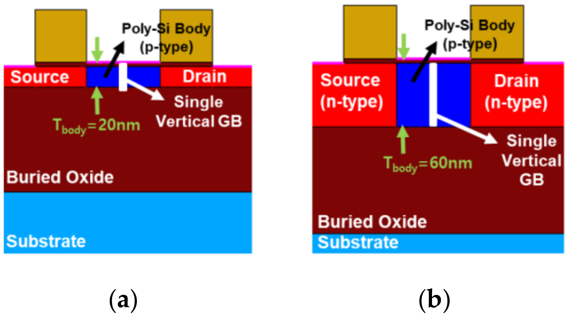
2. Materials and Methods

Simulations were performed with the Sentaurus TCAD tool to examine the dependence of leakage current and transient characteristics on device body thickness and Write”1” drain voltage. Figure 1a,b shows parts of the cross-sections of the simulated poly-Si 1T-DRAM devices with 20 nm and 60 nm body thicknesses. They have the same thickness of buried oxide and substrate. We chose a 20 nm body as typical of a thin-body device, and we chose 60 nm, which is the maximum body thickness for an FD-SOI device, to represent a typical thick-body device. A single GB was located in the center of the channel in order to simplify the simulations which were performed with the parameter values shown in Table 1. We named the devices in Figure 1a,b as Tbody20 nm and Tbody60 nm, respectively.
Figure 2 shows the simulation waveforms; the figure depicts the typical time and bias conditions for these devices according to recent research [11,13,14]. The transient simulation was performed in the order of Hold-Write“0”-Hold-Read“0”-Hold-Write“1”-Hold-Read“1”. During the Write“0” operation, a negative drain voltage was applied for 150 ns to supply electrons. In the Write”1” operation, negative gate and positive drain voltages were applied for 500 ns to generate excess holes from band-to-band tunneling. In several studies, 2.0 V was a typical Write“1” drain voltage, but in our study, the Write “1” drain voltage was set to 0.1 V, 1.0 V, and 2.0 V in order to analyze its effect on the memory cell. In the read operation, a low drain voltage was applied for a non-destructive read, and the gate voltage was set to maximize the sensing margin of each cell. Thus, the gate voltages for Tbody20 nm and Tbody60 nm were different; 1.1 V was applied to Tbody20 nm and 1.2 V to Tbody60 nm. During the hold operation, both the gate and the drain were set to 0 V to maintain the data state. Although 10 ns is shown to be the typical hold time in Figure 2, the hold time was varied in order to examine the retention characteristics. The bias and time conditions used in the transient simulation are summarized in Table 2.
The inset in Figure 3 shows the density of the states used in the simulations based on recent research [12,13,14]. In [12], the investigator confirmed the energy band changes’ dependence on the donor and acceptor trap density; the donor traps had little influence on the energy band peak while acceptor traps were proportional to the energy band peak. Moreover, in our previous study [13], we investigated the effect of the capture cross-section on memory characteristics; the capture cross-section is defined as the probability of capturing carriers in the GB. The trap density, trap energy level, and capture cross-section were chosen based on this research, as shown in the Figure 3 inset. The red lines represent the donor traps, and the black lines represent the acceptor traps. In the tails of the conduction band and the valance band, the trap densities had an exponential distribution, and near the mid-gap, they had a Gaussian distribution.
Figure 3 shows the transfer characteristics of TBody20 nm and TBody60 nm. We examined the transfer characteristics for drain voltages of 0.1 V, 1.0 V, and 2.0 V. From Figure 3, Table 3 shows the drain induced barrier lowering (DIBL) and off current (Ioff) for drain voltages of 1.0 V and 2.0 V. DIBL is defined as the threshold voltage (Vth) difference between a 0.1 V and a 1.0 V or 2.0 V drain; Vth is the gate voltage for a drain current of 0.5 µA. Ioff is the drain current when the gate voltage is 0 V. As shown in Table 3, the Ioff and DIBL of the two devices are 80 times and 2.7 times different at a 2.0 V drain voltage, respectively, but for a 1.0 V drain, the differences are 8 times and 1.2 times. Therefore, if the drain operating voltage can be lowered, the SCEs of the thick-body device will not deteriorate significantly.

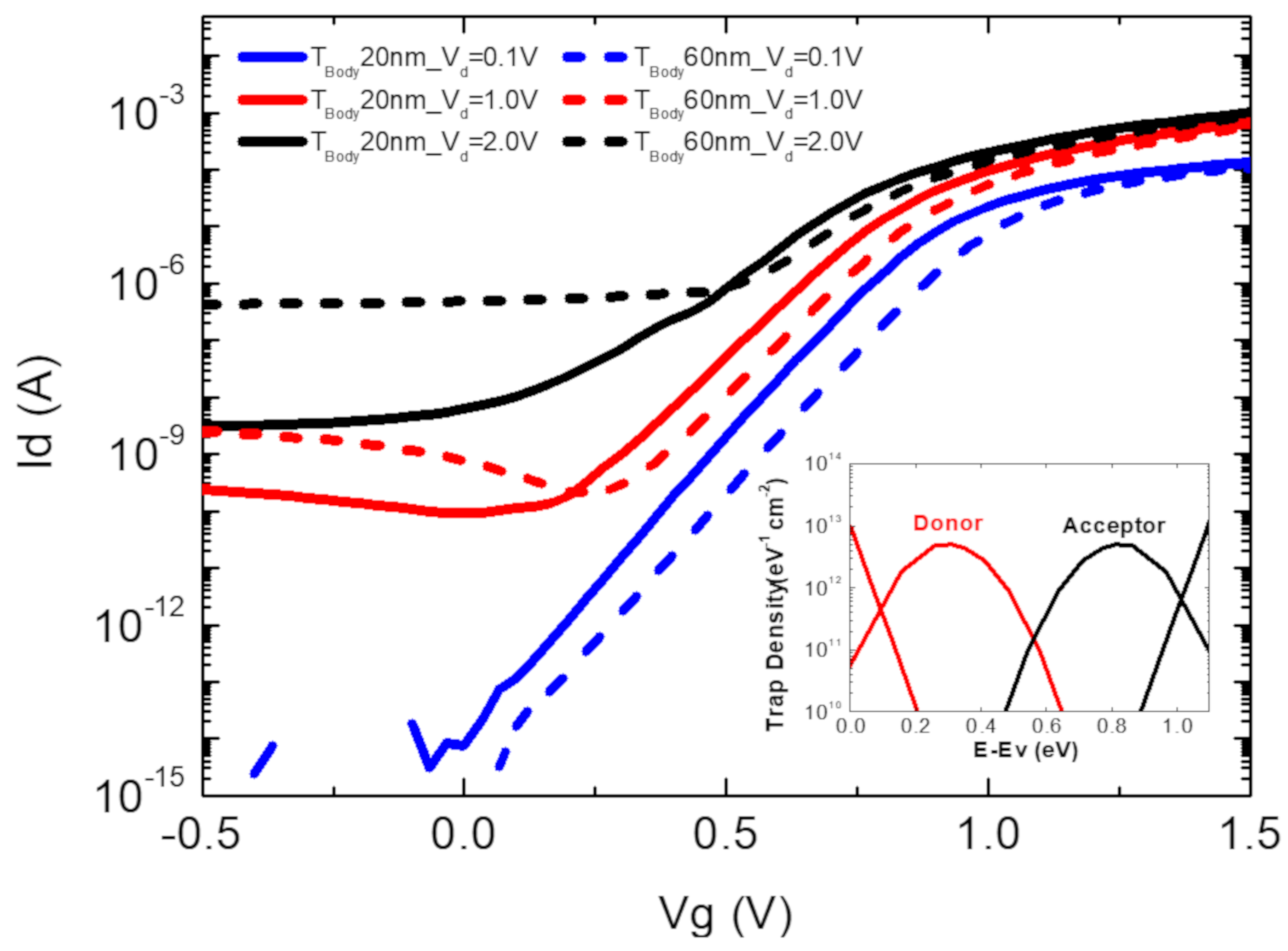
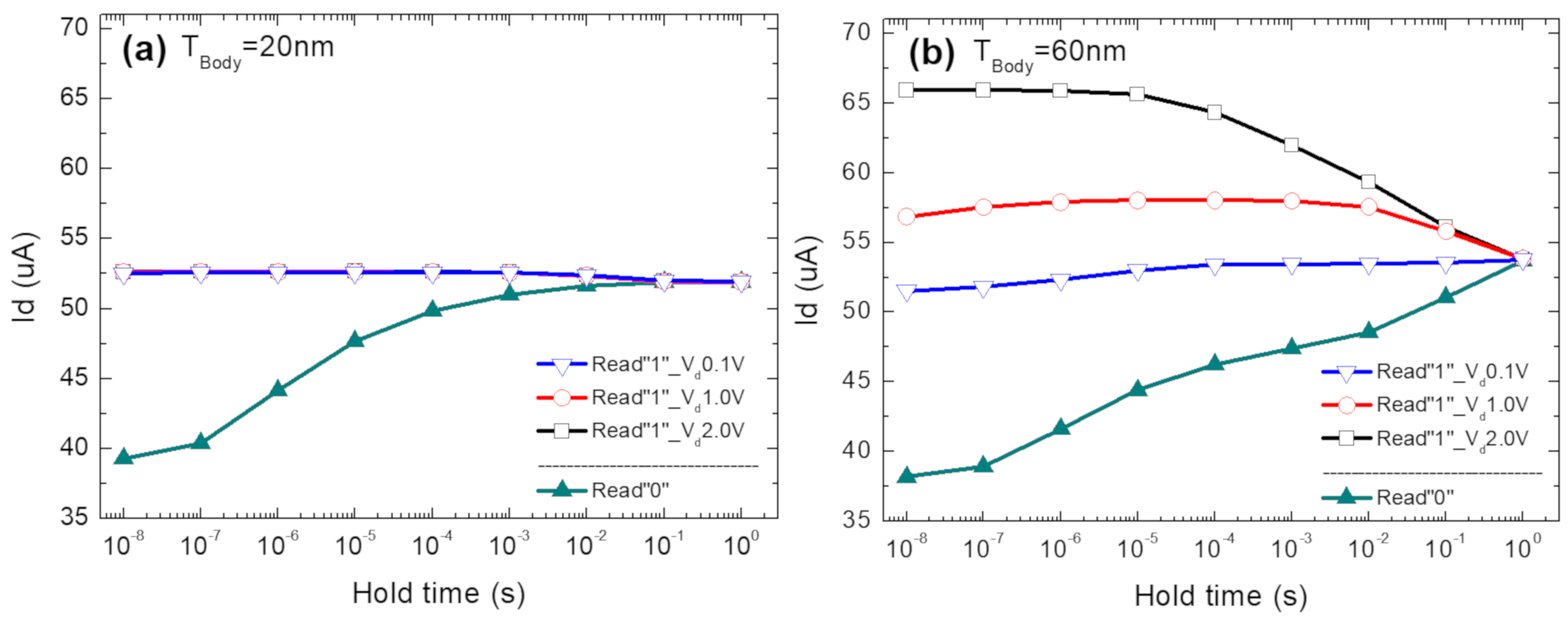
3. Results and Discussion

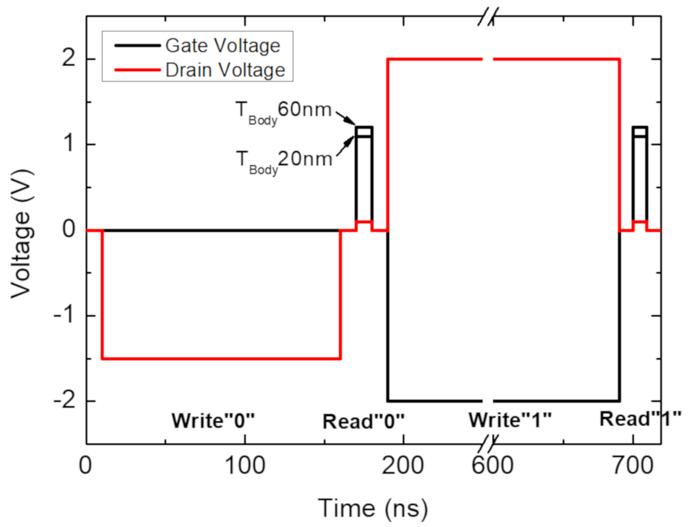
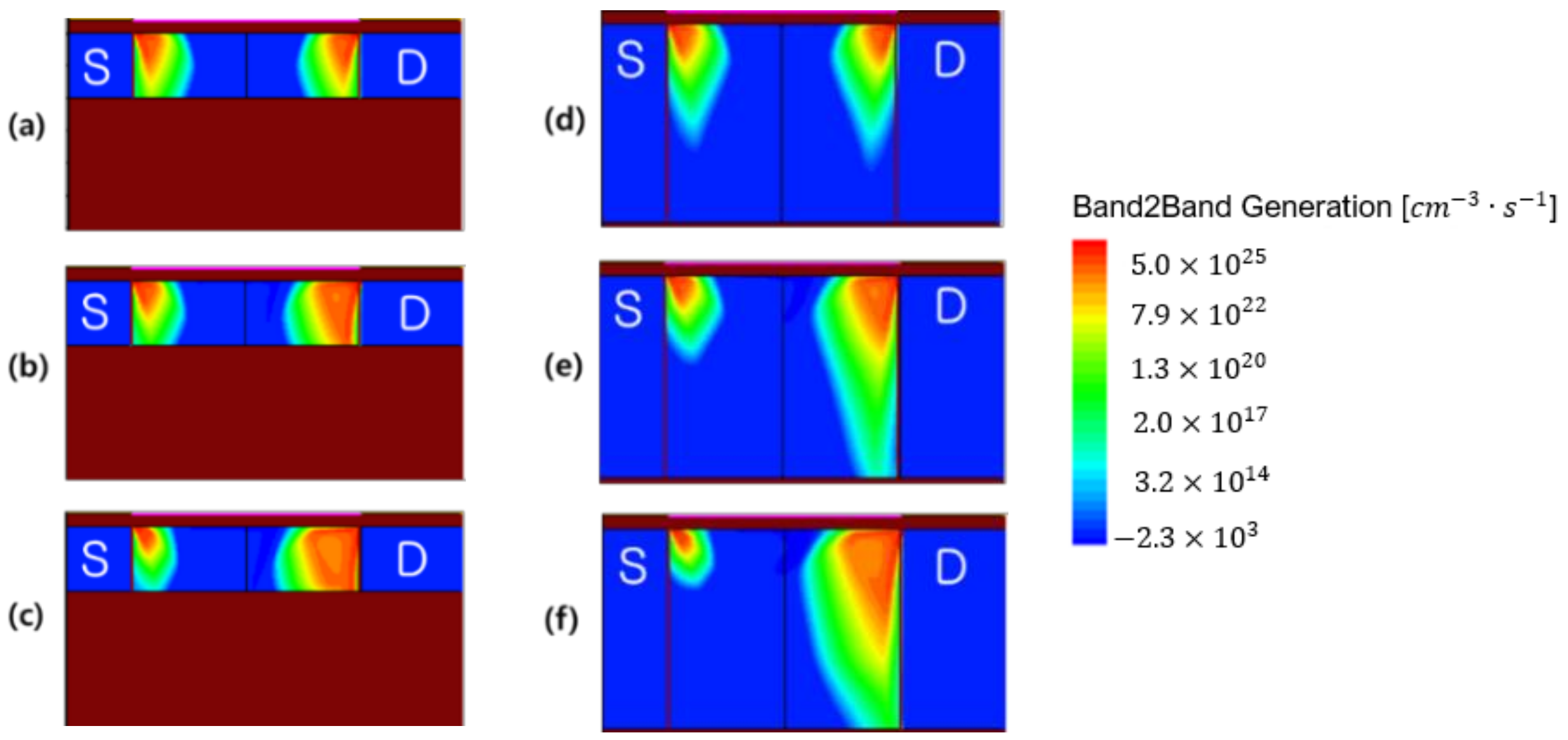
3.1. Transient Characteristics of a Poly-Si 1T-DRAM

Figure 4a,b shows the transient characteristics of memory cells for three Write“1” drain voltages. The figures illustrate the change in read current as a function of the hold time. The solid and open symbols indicate the read current after writing “0” and “1”, respectively. The Write“0” voltage is constant, while the three Write“1” drain voltages have the values 0.1 V, 1.0 V, and 2.0 V. Thus, the Read“0” current has a single value and the Read“1” currents are represented by three values. We named the cells with the three Write“1” operating drain voltages as Vd0.1 V, Vd1.0 V, and Vd2.0 V, respectively.
As shown in Figure 4a,b, the Read“1” current of TBody20 nm is almost constant regardless of the Write“1” drain voltage, while the Read“1” current of TBody60 nm increases in proportion to the Write“1” drain voltage. The band-to-band generation rates and trapped charge density were investigated to determine the cause of the Read“1” current trends.
Figure 5a–f shows two-dimension contours representing the band-to-band generation rates during the Write“1” operation. The three Write “1” drain voltages were applied to each cell in the figures. The band-to-band generation rates can be seen to be in proportion to the Write“1” drain voltage in both TBody20 nm and TBody60 nm, which means that the generated hole charges in the Write“1” operation are also in proportion to the Write“1” drain voltages. The total hole charge trapped in the GB of the two cells with varied a Write“1” drain voltage was also examined in Figure 6.
Figure 6 shows that TBody20 nm has less trapped hole charge than TBody60 nm for all Write“1” voltages because it has less GB regions. Additionally, the trapped hole charge of TBody20 nm is almost uniform, regardless of the Write“1” drain voltage, while TBody60 nm’s trapped hole charge is in proportion to the Write“1” voltage. This means that TBody20 nm cells have difficulty in trapping hole charge, independent of how much excess hole charge is generated by the Write“1” operation. Figure 7 also represents TBody20 nm’s difficulty in trapping holes compared to TBody60 nm.
Figure 7 shows trapped electron and hole charge concentrations as a function of position in the GB when the drain voltage is 1.0 V. The dashed and solid lines indicate TBody20 nm and TBody60 nm, respectively. In both TBody20 nm and TBody60 nm, the trapped electron charge increases and the trapped hole charge decreases as the position in the GB approaches the channel. This trend is due to the inversion charge in the read operation. For a given position in the GB, TBody20 nm has less trapped hole charge and more trapped electron charge than TBody60 nm.
We examined the energy band during the read operation in a vertical cut to determine the cause of the trapped charge concentration trends. Figure 8a,c show the energy bands of TBody20 nm and TBody60 nm in a vertical cut for a read operation after a 10 ns hold time and a Write“1” drain voltage of 1.0 V. Figure 8a,c show the conduction band (Ec), valance band (Ev), electron Fermi level (Fn), and hole Fermi level (Fp). The dashed lines in Figure 8a represent the connection of the band energy from the 20 nm point. In both TBody20 nm and TBody60 nm, the Ec and Ev are bent near the gate electrode because a positive voltage for inversion was applied in the read operation.
Moreover, Fp is lower than Fn due to the excess holes generated by the Write“1” operation. Figure 8b,d show the trap density distributions. The x-axis indicates the acceptor and donor trap density and the y-axis indicates band energy. The acceptor traps are negatively charged when electrons are captured, while the donor traps are positively charged when electrons are emitted. Thus, the electrons with energies below Fn are trapped in the acceptor traps and have a negative charge, and the holes with energies above Fp are trapped in the donor traps and have a positive charge. In the figures, the shaded black area represents the energy region capable of trapping electrons, and the shaded red area is the region that can trap holes. The electron-trapping energy region is the acceptor trap region that is below Fn. Similarly, the hole-trapping energy region is the donor trap region that is above Fp. As can be seen in Figure 8a,c, the difference between the Ec and Fn of TBody20 nm is smaller than that of TBody60 nm; this is because the entirety of TBody20 nm’s thin body is affected by its positive gate voltage, resulting in its lowered Ec and Ev. In TBody60 nm, on the other hand, Ec and Ev are not lowered, and Fn is near the mid-gap at the end of the body because the band energies are more affected by oxide or substrate than by the gate electrode due to the device’s thick body. Therefore, TBody60 nm has few electron traps, but TBody20 nm, with its wide acceptor regions, can easily trap electrons. As a result, the trapped electrons recombine with the excess holes, reducing the trapped hole charge regardless of the Write“1” drain voltage in TBody20 nm.

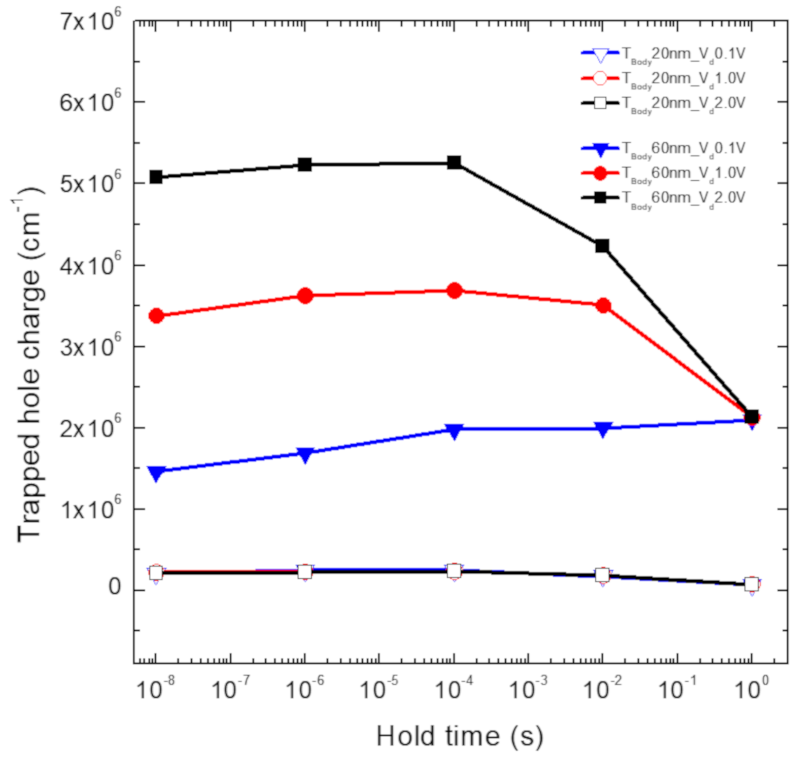
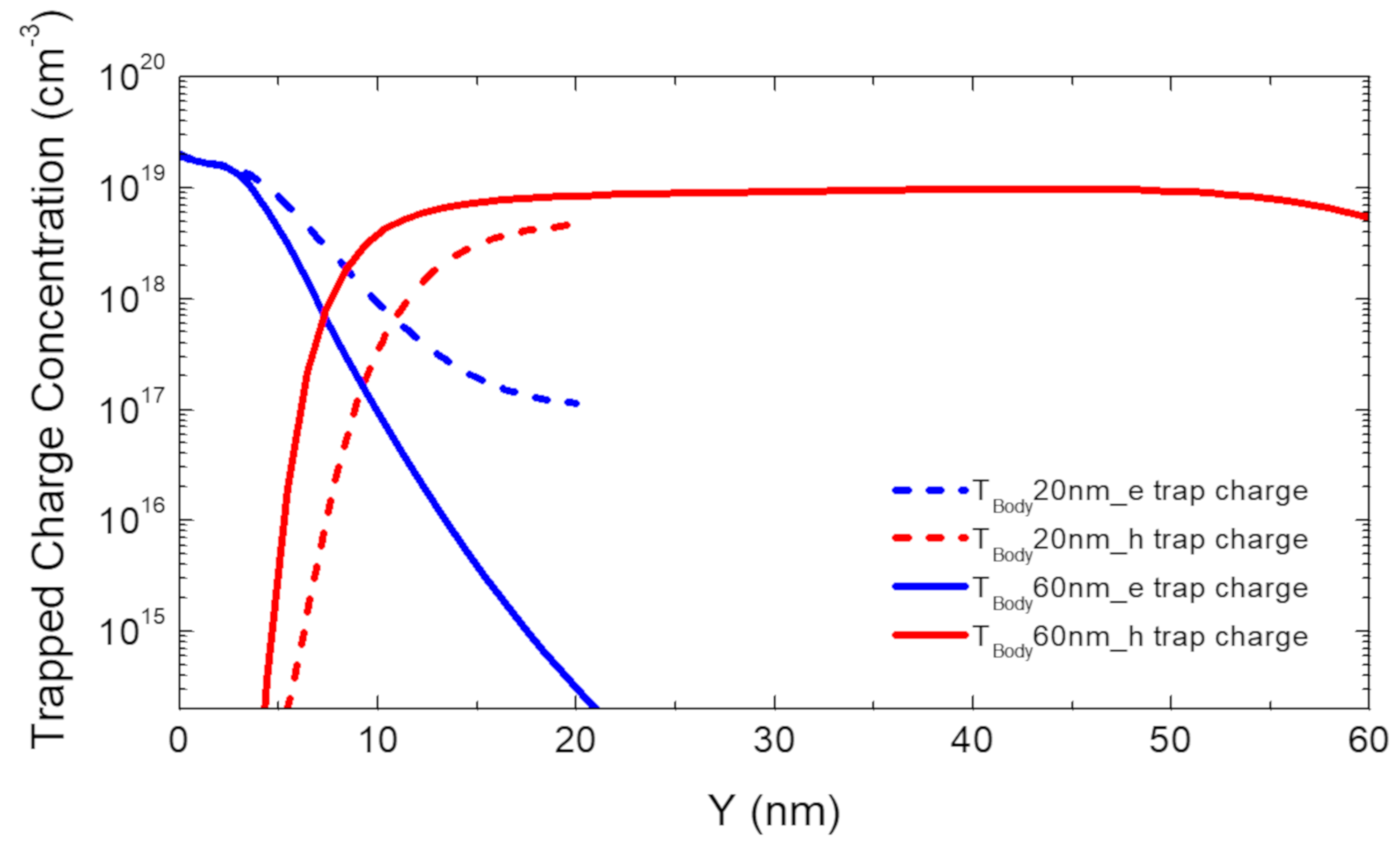
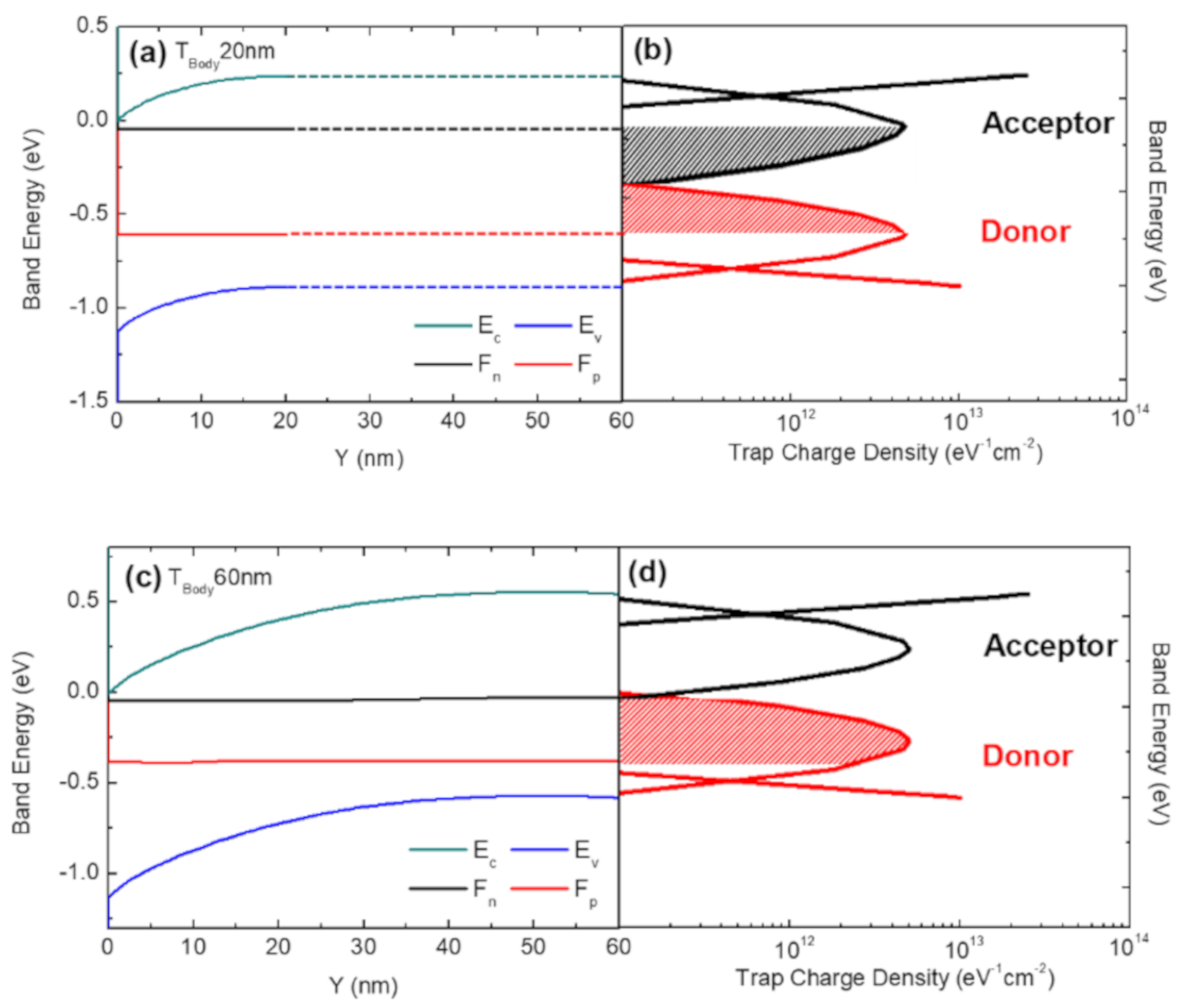
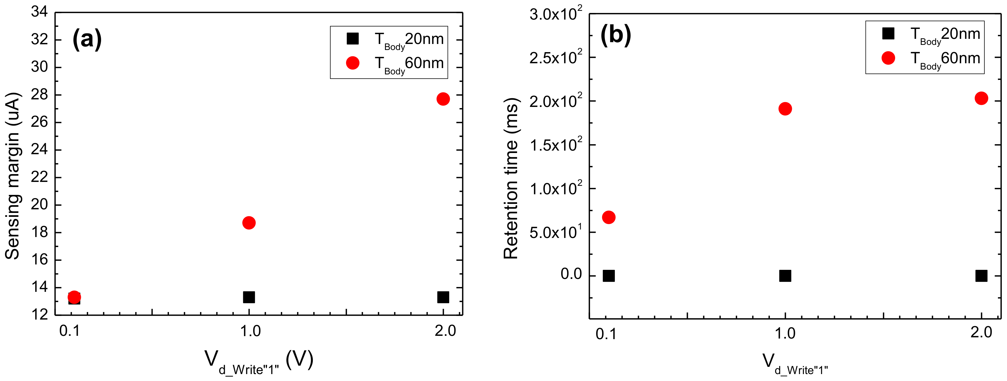
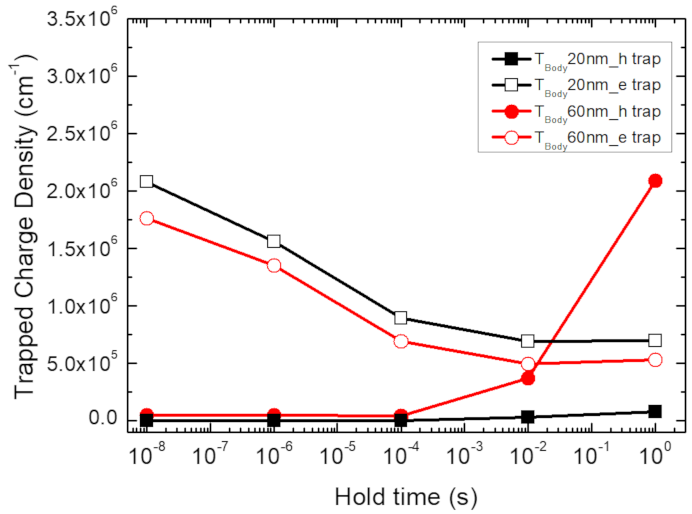
3.2. Operating Performance of a Poly-Si 1T-DRAM

The memory operating performance of TBody20 nm and TBody60 nm was evaluated by observing their sensing margins and retention times. In this paper, the sensing margin is defined as the read current difference between the “1” and “0” states for a 10 ns hold time, and the retention time is defined as the hold time when the current difference reaches 3 uA; 3 uA is the minimum value for detecting the current difference [7]. Figure 9a,b shows the sensing margins and retention times of the two devices for three Write“1” drain voltages. Since the Read“1” current of TBody20 nm has a constant value regardless of its Write“1” drain voltage, the sensing margin and retention time are also constant. On the other hand, the sensing margins and retention times of TBody60 nm vary with the Write“1” drain voltage because the Read“1” current of TBody60 nm is proportional to its Write“1” drain voltage.
The sensing margin increases linearly with the increasing Read“1” current and Write“1” drain voltage, but the retention times do not change significantly for Write”1” drain voltages between 1.0 V and 2.0 V. This is because the Read“1” currents of TBody60 nm for Vd1.0 V and Vd2.0 V are almost the same when the hold time is larger than 0.01 s, as can be seen in Figure 4b. In Figure 6, the difference between TBody60 nm’s trapped hole charges for Vd1.0 V and Vd2.0 V rapidly decreases beyond a 0.01 s hold time. This convergence is due to the rapidly de-trapped hole charge over time. The retention times of TBody60 nm cells are significantly larger than those of TBody20 nm cells even when the sensing margin of both devices is the same, as shown in Figure 9a,b.
We analyzed the trapped charge density in the Read“0” operation to determine why the retention time of TBody60 nm is larger than that of TBody20 nm when the Write”1” drain voltage is 0.1 V. Figure 10 shows the trapped charge of TBody20 nm and TBody60 nm in the Read“0” operation when the Write“1” drain voltage is 0.1 V. The black and red lines represent TBody20 nm and TBody60 nm, respectively, and the solid and open symbols represent the trapped hole and electron charge. At a 10 ns hold time, the trapped electron charge is larger than the trapped hole charge regardless of the body thickness, because the electrons were supplied by the negative drain bias during the Write“0” operation. This trapped electron charge gradually decreases over time due to electron de-trapping. As a result, the Read“0” current of both TBody20 nm and TBody60 nm increases as the trapped electron charge decreases. However, the trapped hole charge’s trend is significantly different depending on the body thickness. In TBody60 nm, the trapped hole charge gradually increases, and when the hold time is 1 s, the trapped hole charge is larger than the trapped electron charge while TBody20 nm retains its initial small trapped hole charge. This increases the “0” current of TBody60 nm even at the hold time of 1 s with little change in trapped electron charge. Therefore, TBody60 nm can operate as a memory for a long time relative to TBody20 nm, because hole trapping occurs even after electron de-trapping is over.
By investigating the energy band during the read operation, we observed that the Write“1” drain voltage had no influence on the Read“1” current of TBody20 nm but greatly affected that of TBody60 nm. Moreover, we found that the sensing margin and retention time of the TBody60 nm cells are larger than that of the TBody20 nm cells due to the hole trapping effect occurring in both the Read“1” and Read“0” states of the TBody60 nm cell. At a 1.0 V Write“1” drain voltage, the TBody60 nm sensing margin is 1.4 times larger than that of TBody20 nm, and, at a 2.0 V drain voltage, it is 2.1 times larger. The retention time of TBody60 nm is at least 1000 times larger than that of TBody20 nm under all Write“1” drain voltage conditions. Therefore, the body thickness and Write“1” voltage fabrication and application conditions of the poly-Si 1T-DRAM cell should be determined considering both SCEs and the memory operating performance.

4. Conclusions

This study reports that the SCEs and the transient operating performance are tradeoffs in poly-Si 1T-DRAM cells with different body thicknesses. Compared to TBody60 nm, TBody20 nm is advantageous for dealing with SCEs, but its sensing margin and retention time are degraded at a typical 2.0 V Write“1” drain voltage. Since SCEs decrease in proportion to the drain voltage, the transient operating performance of TBody20 nm and TBody60 nm were compared as the Write “1” drain voltage was lowered.
TBody60 nm’s operating performance is better than that of TBody20 nm because TBody60 nm can trap more hole charge in both the “1” and “0” states. Since gate biasing affects the entire body of TBody20 nm and bends the energy bands in the Read“1” operation, TBody20 nm has difficulty trapping hole charge regardless of its Write“1” drain voltage. However, the bottom end of TBody60 nm is affected by a buried oxide or silicon substrate and keeps the band flat, so it can trap more holes in its body than TBody20 nm.
In summary, we confirmed that the operating performance of the TBody60 nm cells is better than that of TBody20 nm, even at low Write“1” drain voltages; this means that the SCEs and the operating performance of the memory cell can be considered simultaneously by adjusting the body thickness and the Write “1” operating voltage. We conclude that an optimization method that incorporates the body thickness and voltage conditions of the short channel poly-Si 1T-DRAM should be part of the design, fabrication, and application of this memory cell.

Author Contributions

Conceptualization, S.Y. and H.S.; methodology, W.-K.S.; funding acquisition, H.S.; investigation, S.Y., and W.-K.S.; resources, writing—Original draft preparation, S.Y.; writing—Review and editing, S.Y. and W.-K.S.; supervision, W.-K.S. and H.S. All authors have read and agreed to the published version of the manuscript.

Funding

This work was supported by the Ministry of Trade, Industry and Energy under Grant 10080513 and RP-Grant 2019 of Ewha Womans University. This research was also supported by the Basic Science Research Program through the National Research Foundation of Korea (NRF) funded by the Ministry of Education, Science and Technology (No. 2019R1A2C1084063).

Conflicts of Interest

The authors declare no conflict of interest.

References

  1. Nitayama, A.; Kohyama, Y.; Hieda, K. Future directions for DRAM memory cell technology. In Proceedings of the International Electron Devices Meeting 1998. Technical Digest (Cat. No.98CH36217), San Francisco, CA, USA, 6–9 December 1998; pp. 355–358. [Google Scholar] [CrossRef]
  2. Okhonin, S.; Nagoga, M.; Sallese, J.M.; Fazan, P. A SOI capacitor-less 1T-DRAM concept. In Proceedings of the 2001 IEEE International SOI Conference. Proceedings (Cat. No.01CH37207), Durango, CO, USA, 1–4 October 2001; pp. 153–154. [Google Scholar] [CrossRef]
  3. Okhonin, S.; Nagoga, M.; Sallese, J.M.; Fazan, P. A capacitor-less 1T-DRAM cell. IEEE Electron Device Lett. 2002, 23, 85–87. [Google Scholar] [CrossRef]
  4. Ohsawa, T.; Fujita, K.; Higashi, T.; Iwata, Y.; Kajiyama, T.; Asao, Y.; Sunouchi, K. Memory design using a one-transistor gain cell on SOI. IEEE J. Solid State Circuits 2002, 37, 1510–1522. [Google Scholar] [CrossRef]
  5. Ranica, R.; Villaret, A.; Malinge, P.; Gasiot, G.; Mazoyer, P.; Roche, P.; Candelier, P.; Jacquet, F.; Masson, P.; Bouchakour, R.; et al. Scaled IT-Bulk devices built with CMOS 90 nm technology for low-cost eDRAM applications. In Proceedings of the Digest of Technical Papers. 2005 Symposium on VLSI Technology, Kyoto, Japan, 14–16 June 2005; pp. 38–39. [Google Scholar] [CrossRef]
  6. Tack, M.R.; Gao, M.; Claeys, C.L.; Declerck, G.J. The multistable charge-controlled memory effect in SOI MOS transistors at low temperatures. IEEE Trans. Electron Devices 1990, 37, 1373–1382. [Google Scholar] [CrossRef]
  7. Jeong, H.; Song, K.-W.; Park, I.H.; Kim, T.-H.; Lee, Y.S.; Kim, S.-G.; Seo, J.; Cho, K.; Lee, K.; Shin, H.; et al. A New Capacitorless 1T DRAM Cell: Surrounding Gate MOSFET With Vertical Channel (SGVC Cell). IEEE Trans. Nanotechnol. 2007, 6, 352–357. [Google Scholar] [CrossRef]
  8. Song, K.W.; Jeong, H.; Lee, J.W.; Hong, S.I.; Tak, N.K.; Kim, Y.T.; Choi, Y.L.; Joo, H.S.; Kim, S.H.; Song, H.J. 55 nm capacitor-less 1T DRAM cell transistor with non-overlap structure. In Proceedings of the 2008 IEEE International Electron Devices Meeting, San Francisco, CA, USA, 15–17 December 2008. [Google Scholar] [CrossRef]
  9. Lee, C.-W.; Ran, Y.; Ferain, I.; Kranti, A.; Akhvan, N.D.; Razavi, P.; Yu, R.; Colinge, J.P. Nanowire Zero-Capacitor DRAM Transistors with and without Junctions. In Proceedings of the 10th IEEE International Conference on Nanotechnology, Seoul, Korea, 7–20 August 2010; pp. 242–245. [Google Scholar] [CrossRef]
  10. Chen, Y.-T.; Sun, H.-C.; Huang, C.-F.; Wu, T.-Y.; Liu, C.W.; Hsu, Y.-J.; Chen, J.-S. Capacitorless 1T Memory Cells Using Channel Traps at Grain Boundaries. IEEE Electron Device Lett. 2010, 31, 1125–1127. [Google Scholar] [CrossRef]
  11. Kim, M.-S.; Cho, W.-J. Capacitorless 1T-DRAM on Crystallized Poly-Si TFT. J. Nanosci. Nanotechnol. 2011, 11, 5608–5611. [Google Scholar] [CrossRef] [PubMed]
  12. Baek, M.-H.; Lee, S.-H.; Kwon, D.W.; Seo, J.Y.; Park, B.-G. Hole Trapping Phenomenon at the Grain Boundary of Thin Poly-Si Floating-Body MOSFET and Its Capacitor-Less DRAM. Appl. J. Nanosci. Nanotechnol. 2017, 17, 2906–2990. [Google Scholar] [CrossRef]
  13. Kim, H.-J.; Kang, I.-M.; Cho, S.-J.; Sun, W.-K.; Shin, H.-S. Analysis of operation characteristics of junctionless poly-Si 1T-DRAM in accumulation mode. Semicond. Sci. Technol. 2019, 34, 105007. [Google Scholar] [CrossRef]
  14. Kim, H.-J.; Yoo, S.-Y.; Kang, I.-M.; Cho, S.-J.; Sun, W.-K.; Shin, H.-S. Analysis of the Sensing Margin of Silicon and Poly-Si 1T-DRAM. Micromachines 2020, 2, 228. [Google Scholar] [CrossRef] [PubMed] [Green Version]
  15. Jang, W.-D.; Yoon, Y.-J.; Cho, M.-S.; Jung, J.-H.; Lee, S.-H.; Jang, J.-W.; Bae, J.-H.; Kang, I.-M. Polycrystalline silicon metal-oxide-semiconductor field-effect transistor-based stacked multi-layer one-transistor dynamic random-access memory with double-gate structure for the embedded systems. Jpn. Soc. Appl. Phys. 2020, 59. [Google Scholar] [CrossRef]
  16. Yoon, Y.-J.; Seo, J.-H.; Cho, S.-J.; Lee, J.-H.; Kang, I.-M. A polycrystalline-silicon dual-gate MOSFET-based 1T-DRAM using grain boundary-induced variable resistance. Appl. Phys. Lett. 2019, 114. [Google Scholar] [CrossRef]
  17. Seo, J.-H.; Yoon, Y.-J.; Yu., E.-S.; Sun, W.-K.; Shin, H.-S.; Kang, I.-M.; Lee, J.-H.; Cho, S.-J. Fabrication and Characterization of a Thin-Body Poly-Si 1T DRAM with Charge-Trap Effect. IEEE Electron Device Lett. 2019, 40. [Google Scholar] [CrossRef]
Figure 1. Parts of cross-sections of the simulated structures of two one-transistor dynamic random-access memory cells using polysilicon body (poly-Si 1T-DRAM) with different body thicknesses: (a) 20 nm and (b) 60 nm.
Electronics 09 01051 g001
Figure 2. Simulation waveforms demonstrating poly-Si 1T-DRAM functionality.
Electronics 09 01051 g002
Figure 3. Id-Vg transfer curve of poly-Si 1T-DRAM cells (inset, the density of states in poly-Si 1T-DRAM).
Electronics 09 01051 g003
Figure 4. Transient characteristics of (a) TBody20 nm and (b) TBody60 nm cells according to drain voltage condition in Write“1”.
Electronics 09 01051 g004
Figure 5. Band-to-band generation rate in Write“1” operation of (a–c) TBody20 nm and (d–f) TBody60 nm cells when the Write”1” drain voltage is (a), (d) 0.1 V, (b), (e) 1.0 V, and (c), (f) 2.0 V.
Electronics 09 01051 g005
Figure 6. Transient hole trap charge density of the TBody20 nm and TBody60 nm devices in the Read”1” operation with varied Write”1” drain voltages.
Electronics 09 01051 g006
Figure 7. Trapped charge concentration in the Read”1” operation according to the GB position in a vertical cut when the Write”1” drain voltage is 1.0 V.
Electronics 09 01051 g007
Figure 8. (a) Energy band in a vertical cut and (b) trap charge densities of TBody20 nm. Moreover, TBody60 nm’s (c) energy band and (d) trap charge densities during the read operation after 10 ns of hold time when the Write“1” operating drain voltage is 1.0 V. The dashed lines in (c) are the connection of the band energy from the 20 nm point. The black and red shaded regions in (c) and (d) represent energy levels capable of trapping electrons and holes, respectively.
Electronics 09 01051 g008
Figure 9. The (a) sensing margin and (b) retention time of TBody20 nm and TBody60 nm for three Write“1” operating drain voltages.
Electronics 09 01051 g009
Figure 10. The trapped charge density of the TBody20 nm and TBody60 nm cells as a function of the hold time in Table 1. Drain voltage is 0.1 V.
Electronics 09 01051 g010
Table 1. Device parameters for poly-Si 1T DRAM simulation.
ParameterValue
Gate Length (Lg)70 nm
Body Thickness (Tbody)20 nm/60 nm
Buried Oxide Thickness (Tbox)100 nm
Substrate Thickness (Tsub)800 nm
Gate Oxide Thickness (Tox)40 Å
Source/Drain Doping Concentration (Arsenic) 1 × 10 20   cm 3
Channel Doping Concentration (Boron) 1 × 10 18   cm 3
Substrate Doping Concentration (Boron) 1 × 10 16   cm 3
Table 2. Bias and time conditions for the transient operation of poly-Si 1T- DRAM cells.
Write“1”Write“0”ReadHold
Vg (V)−201.1 (Tbody20 nm)
1.2 (Tbody60 nm)
0
Vd (V)0.1/1/2−1.50.10
Time (ns)50015010-
Table 3. Drain induced barrier lowering (DIBL) and off region current according to different drain voltage conditions and body thickness of poly-Si 1T-DRAM cells.
TBody20 nm60 nm
Vd1.0 V2.0 V1.0 V2.0 V
DIBL [V]0.1350.3030.1620.806
Ioff [A]9.23 × 10−116.28 × 10−97.7 × 10−104.917 × 10⁻⁷

