1. Introduction
The technology of contactless power transfer is the subject of intense research activity focused on various application areas [
1,
2,
3]. According to the target application, the transmitter and the receiver stages of a WPT system can be coupled capacitively or inductively [
4,
5]. This paper is interested in the exploitation of an inductively coupled WPT system for recharging the on-board batteries of electric vehicles. Dynamic WPT is a challenging solution that, in contrast to stationary WPT, overcomes the inconvenience of having a bulky battery on board the electric vehicles (EVs) as well as the need of long stops for its recharge [
6]. This is achieved by transferring to the in-motion EVs the power to recharge their battery. As a result, the weight (and volume) of the battery can be shrunk and no stops are virtually required for the battery recharge [
7,
8].
Numerous papers on the stationary WPT systems are available in literature, devoted to analyze the functioning of their different components [
9] or to span the whole development of a system [
10,
11]. Apart from some interesting exceptions, such as [
12], the same does not occur for the dynamic WPT systems, likely because the research activities on the matter are more recent. Specifically, most of the papers on the dynamic WPT systems are dealing with either their layout [
13,
14] or their coupling set, i.e., the set made up of the receiving coil (or pickup) located onboard EV and the transmitting coils deployed along the track [
15], or their compensation networks [
16,
17].
The aim of this paper is twofold: (i) to develop a dynamic WPT system committed to charge the battery of an in-motion EV, and (ii) to present such a development in its unfolding, starting from the assessment of the electrical specifications for the dynamic WPT system till to its experimentation on a setup. Focus is on the power stages of the dynamic WPT system, namely the coupling set, conversion and compensation stages. In view of arranging an affordable setup, an EV calling for the power transfer of a few kW is considered as a case study.
In detail, the paper is organized as follows.
Section 2 establishes the design specifications for the dynamic WPT system.
Section 3 illustrates the characteristics of the power stages of the dynamic WPT system; specifically, it illustrates structure of the coupling set, layout of the coils, configuration of the conversion stages and topology of the compensation networks.
Section 4 works out the electrical sizing of the power components of the stages.
Section 5 describes the setup arranged to implement the dynamic WPT system.
Section 6 reports the results of experimental tests that corroborate the design of the dynamic WPT system.
Section 7 concludes the paper.
In the paper, the first-harmonic approximation is used to represent the AC currents and voltages of the dynamic WPT system. Moreover, lower-case letters are used to denote variable quantities whilst upper-case letters denote both constant (or nearly constant) quantities and average values of variable quantities. Lastly, upper-case letters with hut denote magnitude of sinusoidal quantities.
2. Electrical Specifications
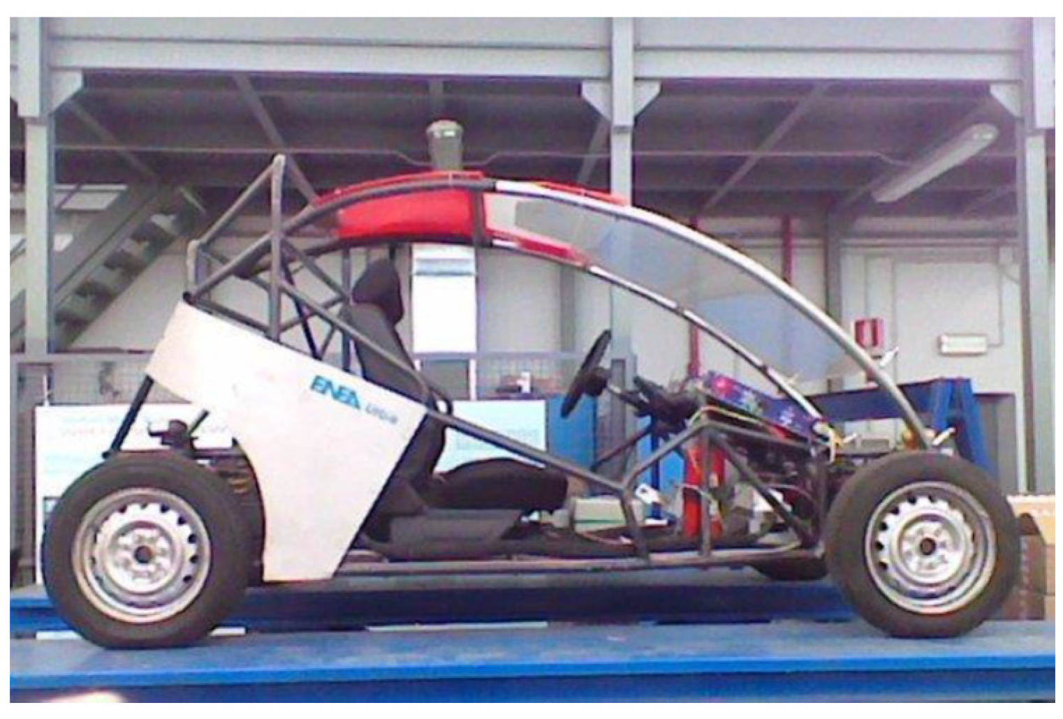
The dynamic WPT system developed in this paper is designed to charge the battery of an EV while it is moving at its maximum speed. As a case study, the vehicle Urbe is taken. Urbe is an electric city-car assembled by ENEA (Italian National Agency for New Technologies, Energy and Sustainable Economic Development) for the accomplishment of various research activities on sustainable mobility [
18]. A picture of Urbe is shown in
Figure 1 and its data are reported in
Table 1. The data include the maximum battery charging power
Pb,max with the corresponding maximum battery voltage
Vb,max.
In order to charge the battery at the maximum charging power, the dynamic WPT system must be sized to transfer onboard both the battery power
Pb, max and the power drawn by the traction drive (TD) to move the vehicle. Such a power is specified for the EV travelling at maximum speed on horizontal road. In these conditions the force necessary to propel the EV is
The first term in (1) is the air drag force whilst the second one is the rolling friction. The value of F in (1) is calculated for an air density ρair of 1.167 kg/m3 and a gravity acceleration g of 9.81 m/s2.
Assigning a confidence value of 0.8 to the overall efficiency
ηtd of TD, the latter draws an electric power of
The overall power drawn by the EV during the in-motion battery charging is then
Power
PEV represents the output power specification for the dynamic WPT system. Additional specifications for the system are as follows: (i) to be fed by a single-phase grid at the voltage
Vg = 230
Vrms, 50 Hz (ii) as per SAE recommendations, to supply the track coils at the angular frequency
ω = 2π × 85,000 rad/s with a tolerance interval ranging from
ω = 2π × 79,000 rad/s to
ω = 2π × 90,000 rad/s. It is worth to note that the power requirement in (3) and the ground clearance given in
Table 1 place the considered dynamic WPT system in the WPT1/Z1 class defined in [
19], which encompasses WPT systems with maximum apparent power of 3.7 kVA and a distance between the transmitting and the receiving coil between 0.1 m and 0.15 m.
3. Dynamic WPT System Power Stages
As for any WPT system, the core power stage of a dynamic WPT system is the coupling set. It is supplemented with conversion stages and compensation networks in both track and pickup sides. The various stages are illustrated below together with the coil layout.
3.1. Coupling Set and Coil Layout
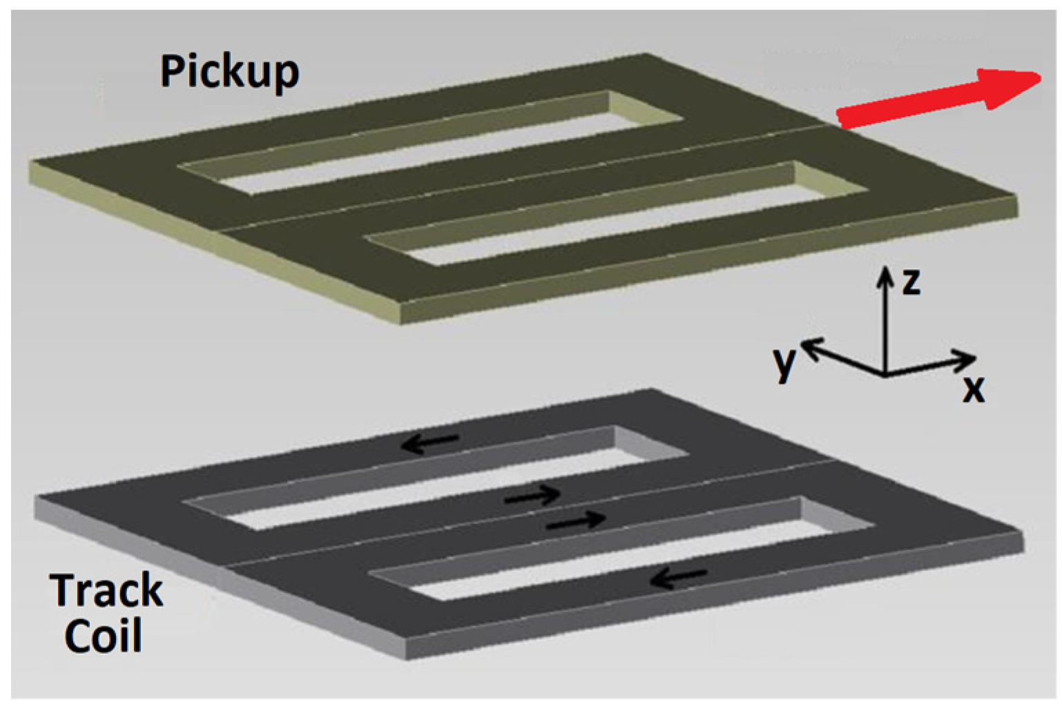
In the developed dynamic WPT system, double D (DD) geometry is utilized for both pickup and track coils because of its superior coupling properties under motion of the pickup [
20,
21]. According to
Figure 2, each DD coil consists of two equal sub-coils deployed side by side, connected in series, and wound in such a way that the vertical flux components have opposite directions at the surface of the two sub-coils.
The track is of lumped type, made of a string of equal DD coils spaced of distance D each other. In order to simplify the design of the overall system and to reduce the production cost of the prototype, the same dimensions have been fixed for the pickup DD coil and the track DD coils, so that the self-inductance
Lp of the pickup coil is equal to that of a track coil L
t. The performance of DD coils is fully exploited if the pickup coil has the same orientation as the track coils, as shown in
Figure 2. The common side of the sub-coils forming the pickup and the track coils is aligned along the x-axis, i.e., the direction of the vehicle motion, to get rid of the zero-coupling point of DD coils and of the consequent need of endowing the pickup with a Q coil [
22]. Such a pickup motion takes advantage of the fact that high-end EVs are nowadays equipped with the so-called lane-keeping advanced driver-assistance system that could be instructed to maintain the EV on the trajectory joining the track coil centers. Otherwise, other solutions could be envisaged, specifically developed for the alignment of the coils of WPT systems [
23].
On the basis of the foregoing choices, the layout of the pickup and the track coils becomes as explicated in
Figure 3. Let track coil a and track coil b situated just ahead and behind the pickup be supplied with sinusoidal currents having the same magnitude
and the same phase. The voltage induced across the pickup has magnitude
given by
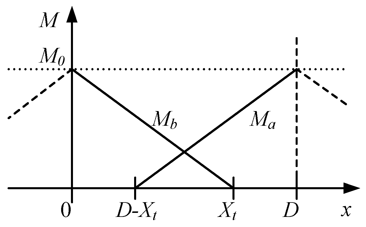
where mutual inductances
Ma(x) and
Mb(x) between pickup and track coils a and b vary with the pickup position
x. In writing (4), only the voltage term due to the flux linkage produced by the current oscillation in the two track coils is accounted for because the voltage term produced by the EV motion is negligible [
24]. For a DD coupling set the mutual inductances are a nearly linear function of
x [
25], and go from maximum value
M0 to zero, according to the profile of
Figure 4. Consequently, if the longitudinal dimension
Xt of the track coils is equal to their distance,
Mb falls to zero when
Ma reaches the maximum
M0, and vice-versa so that, from (4), it turns out that the amplitude of the voltage induced across the pickup is constant and equal to
In the literature [
26], magnitude and phase constraints for the track coil currents are fulfilled by connecting the coils in series and by supplying them through a single high-frequency inverter (HFI); here, it is assumed that each coil is supplied by a separate HFI because this solution is more representative of tracks that extend over long distances and encompass a large number of coils.
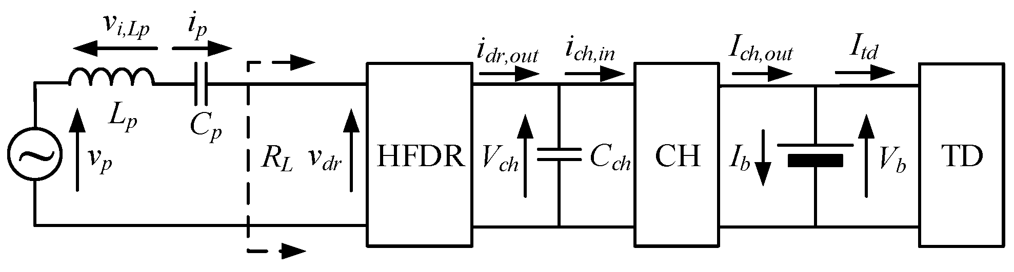
3.2. Pickup Side Conversion Stage
The schematic of the conversion stage in the pickup side is shown in
Figure 5. It consists of the cascade of a high frequency diode rectifier (HFDR) and a chopper (CH), with an in-between DC link whose voltage
Vch is made nearly insensitive to the high frequency content of the currents
idr,out and
ich,in by a suitable value of capacitor
Cch. CH regulates its output voltage at battery voltage
Vb and delivers current
Ich,out to the EV DC bus; in turn, current
Ich,out splits into battery current
Ib and TD current
Itd. Therefore, the actual value of
Ich_out depends on the actual status of the charging process, as well as the speed and acceleration of the vehicle. The power stage, as seen by the pickup coil, is equivalent to load resistance
RL.
The pickup-induced voltage
vp is only partially available for the supply of the downstream conversion stage because of the voltage drop
vi.Lp across the pickup inductance. To make
vp fully available, a compensation network is inserted in the pickup. The simplest and more convenient compensation network is constituted by an in-series capacitor, denoted as
Cp in
Figure 5, sized to resonate with the pickup inductance
Lp at the supply frequency. Further to this solution, the voltage drops across
Lp anc
Cp cancel out each other and hence it is
where
is the magnitude of the first-harmonic component of the voltage at the input of the HFDR. By Equations (5) and (6), it derives that, for any required value of
, the introduction of the resonating capacitor minimizes
and the consequent Joule losses in the track coils [
27,
28].
3.3. Track Side Conversion Stage
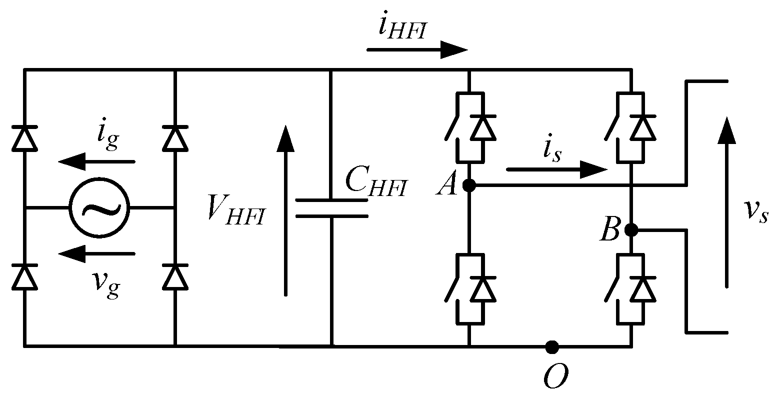
The schematic of the conversion stage in the track side is shown in
Figure 6. A grid diode rectifier (GDR) with capacitive load
CHFI maintains a nearly constant voltage
VHFI at the input of an H-bridge HFI that generated the track coil supply voltage
vs. According to the phase shift technique, the HFI generates two square-wave voltages
vAO and
vBO with 50% duty-cycle and adjustable phase delay
between them. The output voltage
vAB takes the three levels
VHFI, 0, and −
VHFI and its first harmonic component, which is identified with
vs throughout the paper, has a magnitude expressed as
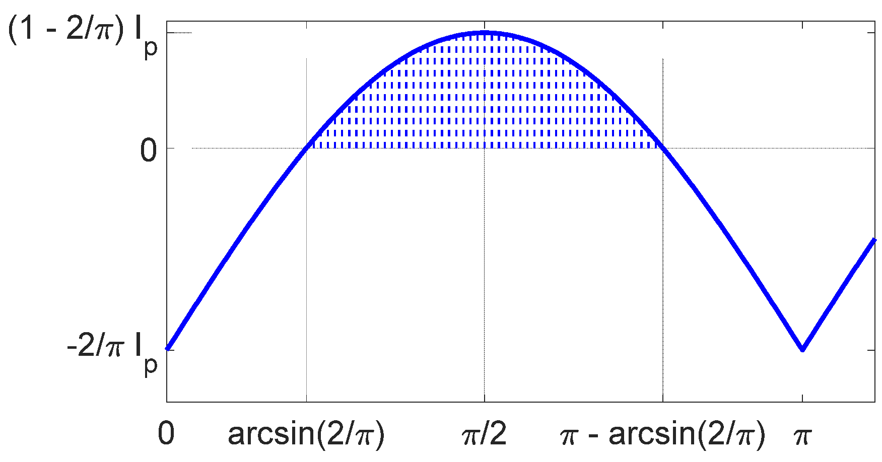
Its minimum value is equal to zero and is obtained setting to zero so that vAO and vBO are in phase, while its maximum value is equal to , reached setting to π so that vAO and vBO are in phase opposition.
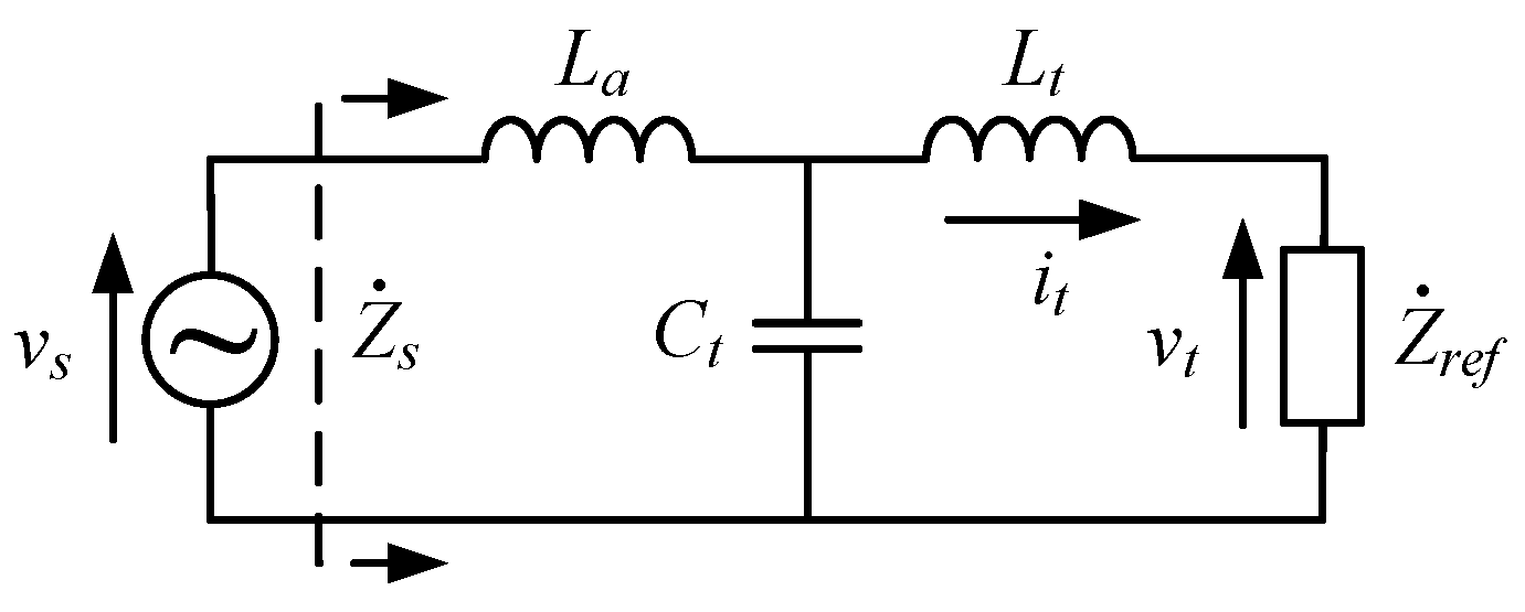
When the pickup lays exactly over the center of a track coil, its equivalent impedance reflected to the track coil is expressed as
and, thanks to the series compensation in the pickup, is purely resistive. In the stationary WPT systems, also the transmitting coil inductance is typically compensated for by an in-series capacitor. Such a compensation is not suitable for the dynamic WPT systems because HFI must react promptly to the variations of the mutual inductance to avoid the flow of excessive currents in the track coils, in particular when the mutual inductance becomes lower than maximum value
M0 and
, according to (8), decreases to zero [
29]. To circumvent this problem, the developed dynamic WPT system uses an inductive capacitive inductive (LCL) compensation for the track coils. The resulting track circuit is shown in
Figure 7, where
La and
Ct are the auxiliary inductor and the capacitor of the compensation network and
vt is the voltage induced across the track coil by current
ip flowing in the pickup.
Value of
La is selected equal to
Lt and that of
Ct is taken for it to resonate with both the circuit inductances at the supply frequency. Then, the impedance seen by HFI is
while the current flowing in the track has magnitude given by
and phase lagging
vs of π/2. When the pickup leaves the track coil center,
M falls below
M0 and, as outlined by (9), the track circuit is not subjected to any overcurrent since
increases; what is more, (10) shows that the track coil is inherently protected from any overcurrent stress since the current flowing in it is imposed by
and is independent from
M.
By Equations (5) and (10), the magnitude of the voltage induced across the pickup is proportional to that of the supply voltage according to
where
k0 is the coupling coefficient between pickup and track coil, calculated for
M = M0; further to the setting of
Lp = Lt,
k0 is given by
M0/Lt.
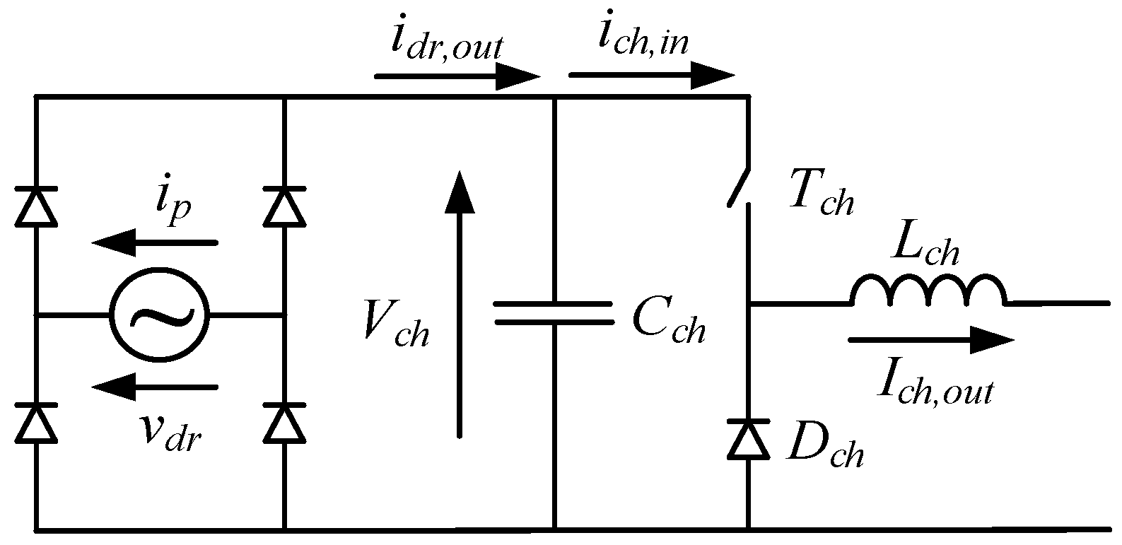
4. Power Stage Electrical Sizing
Besides the output power specification, electrical sizing of the power stages of the dynamic WPT system is essentially determined by the specifications on the type and voltage of the system supply, a single-phase grid at 230
Vrms in this case, and the maximum charging voltage of the EV battery
Vb,max equal to 56 V. The first specification sets the peak of the GDR input voltage at 320 V; the second specification leaves some degree of freedom on selection of voltage
Vch since it depends on the CH type and the voltage level that ensures an acceptable conversion efficiency. Here, a CH of buck type is selected and voltage
Vch is fixed at 65 V, a few volts higher than
Vb,max to account for the voltage drop on CH and to allow it to effectively force the output current. The resultant schematic of the pickup side conversion stage is shown in
Figure 8.
Under the imposed resonance conditions, voltage sizing of the conversion stages is strictly related to the voltage values defined above, whilst voltage sizing of the coupling set is also related to the current flowing in the coils and their inductance. Current sizing of the power components in the two sides is strictly related to mutual inductance M0 and the EV power specification. Lastly, power sizing of the conversion stages is strictly related to the EV power specification whilst that of the coupling set is given by the product of the coil voltage and current sizing.
In the following subsections, electrical sizing of the power components in the stages is based on confidence values of 0.95 for the power converters efficiency ηc and of 0.85 for the efficiency ηcs of the coupling set. In developing the analysis, the not ideal efficiency of the converters is ascribed to the losses caused by the voltage drop across their switches or diodes.
4.1. Track Side Power Component Sizing
4.1.1. High Frequency Inverter
Sizing of the HFI starts from the hypothesis that, thanks to the action of CHFI, the voltage VHFI at the input of the HFI is nearly constant; the minimum value of CHFI needed to achieve this result will be worked out in the next subsection.
By neglecting the voltage drop across the diodes of the GDR, the following relation can be written to find
VHFIConsidering the power
PEV that must be supplied to the EV DC bus and the efficiencies of the HFI, HFDR, CH, and of the coupling set, the average value of
iHFI can be evaluated in
where the first term on the right-hand side corresponds to the power supplied by the GDR.
When the HFI operates at maximum power,
is set to π and, except for the dead times, the output current
is flows for half of the supply period through the upper switch of one leg of the HFI and for the remaining half of the period through the upper switch of the other leg. Under these conditions,
iHFI corresponds to the rectified counterpart of
is that, in turn, is nearly sinusoidal because of the LCL compensation. From this latter condition, considering the relation existing between the amplitude of a sinusoid and the average value of its rectified version, the peak amplitude of
is results in
This is the maximum current flowing in the switches and the diodes that constitute the HFI; these devices must sustain the maximum voltage VHFI.
4.1.2. Grid Diode Rectifier
According to the conventional functioning of a full bridge diode rectifier, the capacitor
CHFI is discharged by the
iHFI current along the full grid period
Tg and every half of
Tg it is recharged for a short time interval by a pulsating current flowing in the diodes of the GDR. Oscillations of
iHFI around its average value
IHFI have a frequency much higher than that of the recharging current and hence their effects on the voltage
VHFI are neglected. Nevertheless,
VHFI is subjected to a ripple Δ
VHFI having twice the grid frequency and originated by the pulsations of the recharging current. By allowing Δ
VHFI to be 5% of
VHFI and under the hypothesis of
CHFI being recharged in a time span negligible with respect to
Tg,
CHFI is sized using the relation
obtained equating the allowed Δ
VHFI to the voltage decrease across
CHFI originated by the constant discharging current
IHFI in the time interval
Tg.
4.2. Pickup Side Conversion Stage Sizing
The resonance condition of the pickup forces the current
ip to flow in the HFDR for the full supply period and alternatively maintains in conduction one of the pair of diodes in the opposite legs of the HFDR tus periodically reversing the connection of
Cch to the input terminals of the HFDR. Then, voltage
vdr is a square wave whose amplitude, because of the voltage drop across the diodes of the HFDR, is a little higher than
Vch. The resonance nullifies the first harmonic component of the voltage across the
Lp-
Cp series so that the voltage
vp induced across the pickup coincides with first harmonic component of
vdr and both have the peak amplitude
with the coefficient 1/
ηc accounting for the voltage drop across the diodes.
The HFDR output current
idr,out is obtained by rectification of
ip, which is sinusoidal. The alternate component of
idr,out flows in capacitor
Cch while its average value
Idr,out coincides with the average chopper input current
Ich,in and can be expressed as the ratio of
PEV to
VchIn this case, 1/ηc accounts for the not ideal efficiency of the chopper.
From Equation (17), the peak amplitude of
ip results in
4.2.1. Chopper
When the battery is discharged, EV DC bus voltage is minimum and the average current at the chopper output reaches its maximum value
Actually, the current
ich,out is not constant but is subjected to a ripple due to the commutation of
Tch. During the off time of the switch, the voltage applied across the filtering inductance
Lch is equal to
Vb; it opposes the current circulation and
ich,out decreases of an amount equal to
where
δ = Vb/Vch is the duty cycle of
Tch and
T is its switching period, set to 100 μs. Equation (20) shows that the current ripple is a decreasing function of
Lch and that it reaches its maximum when
Vb = Vb,min. As a design choice,
Lch is sized to limit Δ
ich,out to 1% of the nominal
Ich,out, i.e., the current at the chopper output when
Vb = Vb,N, and its value is set to
With this selection of Lch, the ripple of Ich,out can be disregarded and consequently Ich,out,max given by (19) corresponds to the maximum current flowing through Tch, Dch and Lch. The maximum voltage across Tch and Dch is Vch while the maximum voltage across Lch is Vb,max.
4.2.2. High Frequency Diode Rectifier
In the diodes of the HFDR flow either the positive or the negative half-wave of ip and consequently they must be sized to sustain the current given by (18). The maximum voltage across the HFDR diodes is Vch.
The voltage
Vch at the output of the HFDR is subjected to some ripple because nor
idr,out neither
ich,in are constant, being the first obtained by rectification of the sinusoidal current
ip and the second switching between zero and
Ich,out according to the condition of the switch
Tch. The two effects are assessed separately to size
Cch. Let’s suppose, at first, that
idr,out is constant and equal to its average value
Idr,out. Then, while the switch
Tch is open,
Cch is charged with a constant current and the voltage
Vch increases of the amount
Like it happened for
Ich,out, the ripple of
Vch is maximum when
Vb = Vb,min. In order to maintain it within 1% of
Vch,
Cch must be at least
with
Idr,out taken from (17).
Actually, the current
ir,out has an alternate component whose waveform is represented in
Figure 9. According to the hypothesis that it flows completely though
Cch, the consequent ripple of
Vch is proportional to the shaded area in
Figure 9 and is equal to
Inserting in (24) the value of Cch found in (23) the voltage ripple results about 0.03% of Vch, so that it can be disregarded without the need of resize Cch to account for the oscillation of idr,out.
4.3. Coupling Set Sizing
Considering the worst operating condition, i.e., the minimum voltage at the HFI input, the maximum voltage magnitude that can be achieved at the HFI output is obtained from (7) by setting
; it is expressed by
where
ηc accounts for the voltage drop across the HFI switches.
Once fixed
by (16) and
by (25), Equation (11) gives the coupling coefficient that makes the power transfer possible. It is worked out in (26)
By Equation (5), the magnitude
is related also to the current magnitude in the track coil. Assuming for
a reasonable value of 12 A, an estimate of the required
M0 is
It is worth considering that Equations (5) and (11), from which Equations (26) and (27) have been derived, are ideal equations that hold only if
ηcs = 1. Thus, if the prototypal WPT system would implement these values of
M0 and
k0, higher voltages and/or current would be required to transfer the requested power. Consequently, the results coming from (26) and (27) must be considered as the lowest values of
M0 and
k0 that assure the feasibility of the project; together with the maximum dimensions available for the pickup reported in
Table 1 they constitute the specifications for the coupling set.
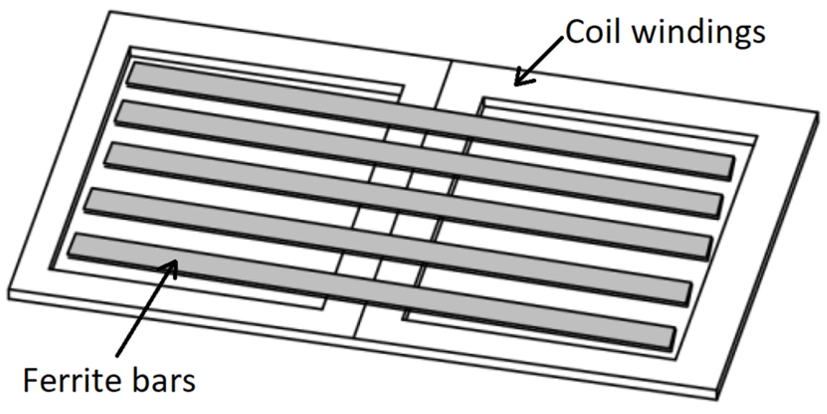
The coils design started by selecting the pickup width. It has been set to 0.95 m, in order to have a good tolerance to lateral misalignment and at the same time to leave a 0.1 m empty space around the coil for its fitting to the vehicle chassis. The same width has been set for the track coils a well.
A number of FEM simulation have been carried out considering different coils length and windings with different number of turns in order to find the combination that best fit the specifications. In the first runs of the simulation, cores made of ferrite plates having the same dimensions of the windings have been considered; then cores made of separate bars have been simulated to optimize the design from the point of view of the required quantity of ferrite [
10].
At the end of this process, the coil with the characteristics reported in
Table 2 and the layout shown in
Figure 10 has been selected both as pickup and track coil.
The current in the pickup is given by Equation (18) while that relevant to the track coil is obtained from (5) using
given by (16) and
M0 coming from the simulations. The total voltage
vLp across the pickup is the phasor sum of the induced voltage
vp and of the inductive voltage drop; because of the resonant compensation, they are in quadrature so that the magnitude
results
The same consideration holds also for the track coils, which are subjected to a total voltage having magnitude
4.4. Compensation Networks Sizing
The components of the compensation networks are readily sized using the values of
Lp and
Lt reported in
Table 2. Both
Cp and
Ct have a capacity of 65 nF while
La has an inductance of 54 μH. Inductor L
a is flown by the current
; capacitors
Cp and
Ct are flown by the currents
and
, the latter one is given by Equation (30), obtained solving the electrical equations of the circuit in
Figure 7.
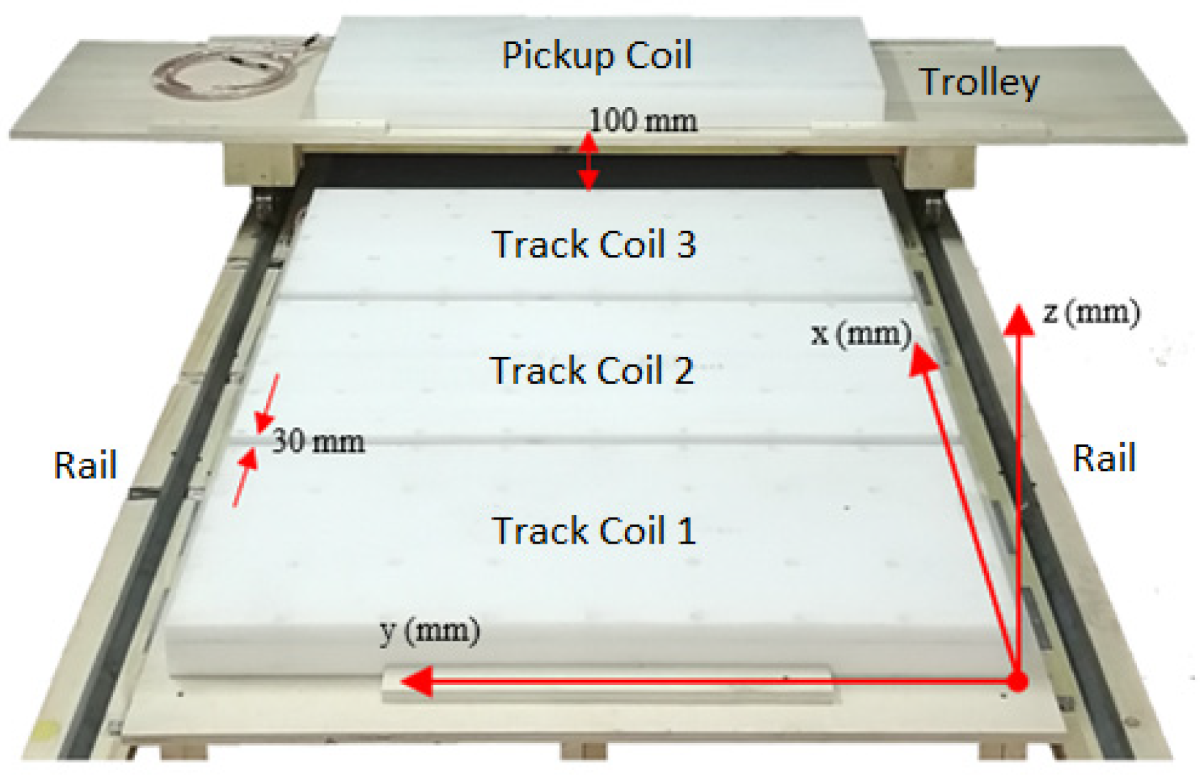
5. Prototype Setup
A full-scale prototype of the proposed WPT system has been designed and manufactured. To comply with the dimensions of the laboratory and to allow a simple connection of the instrumentation to the prototype, a short track made up of three coils has been set up. Each of them are deployed at 30 mm from the other. The pickup coil is carried by a trolley that simulates the electric vehicle and runs over two rails that pair the track coils, as reported in
Figure 11.
According with the design procedure of
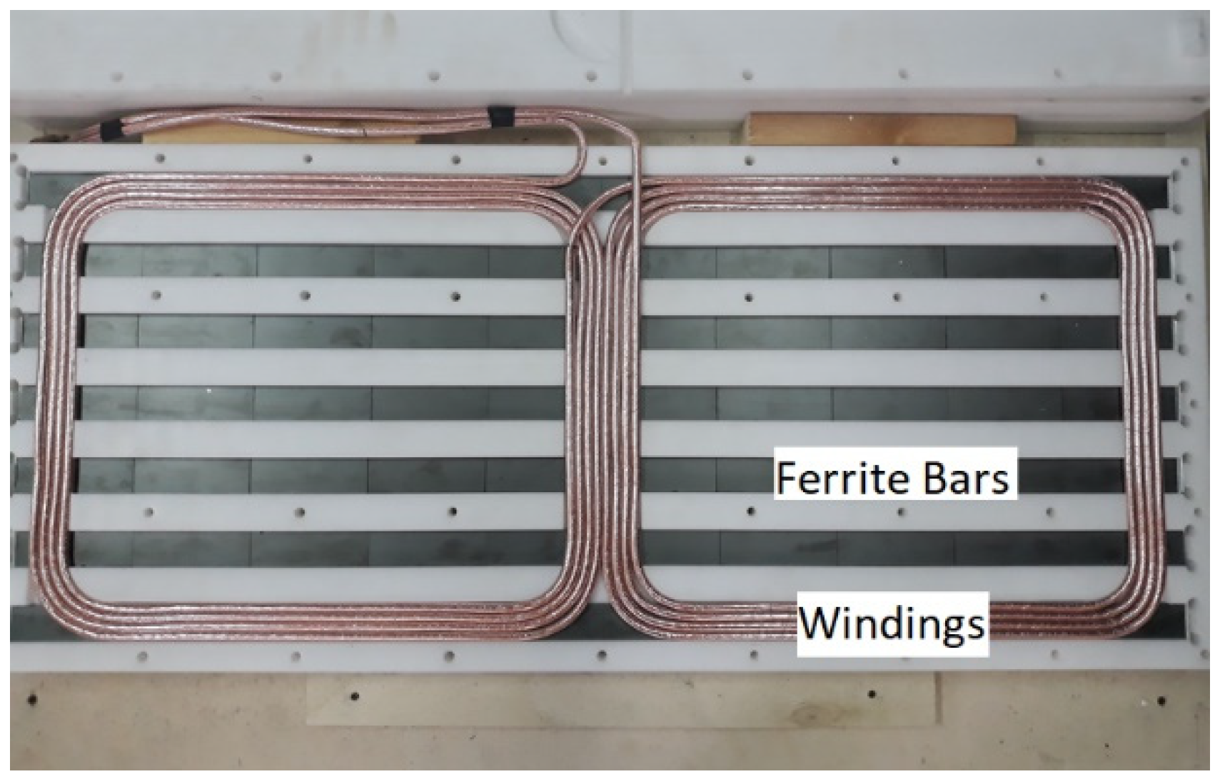
Section 4.3, the same geometry for the pickup and the track coils have been adopted. Polyoxymethylene (POM) base plate has been used for the housing of the winding, made of Litz wire, and of the core, made of seven ferrite bars, each composed by 10 rectangular plates produced by TDK and having the part number B67345B0003X087 I 93/28/16.
Figure 12 shows the inner arrangement of the winding and of the cores of a coil.
As explained in
Section 3.3, each of the compensation networks of the track coils are composed of the auxiliary inductor
La and of the resonant capacitor
Ct. The capacitor has been realized using a combination of EPCOS B32653 6.8 nF capacitors, arranged in such a way to sustain the voltage and current solicitation besides achieving the required capacitance. Theoretically, a good approximation of the resonant capacitance is reached connecting in series two strings of 18 parallel capacitors; however, due to the manufacturing tolerance of the 6.8 nF capacitors, of the auxiliary inductors
La and of the coils, it has been found experimentally that the compensation networks resonate at the nominal supply frequency when only 16 capacitors are connected in parallel to form the two strings, as can be seen analyzing
Figure 13. The series resonant capacitor of the pickup coil, denoted as
Cp in
Figure 14, has been implemented by means of the same configuration of EPCOS B32653 6.8 nF capacitors that has been used for the track coils. Small differences between the capacitances and the inductances of the elements of the three compensation networks are unavoidable, but fortunately it has been demonstrated that they do not affect so much the expected performance of the WPT system, at least for what concerns its efficiency [
30].
The GDR, the HFIs, the HFDR, the CH, and the compensation network have been dimensioned according to the voltage and current amplitudes worked out in
Section 4.
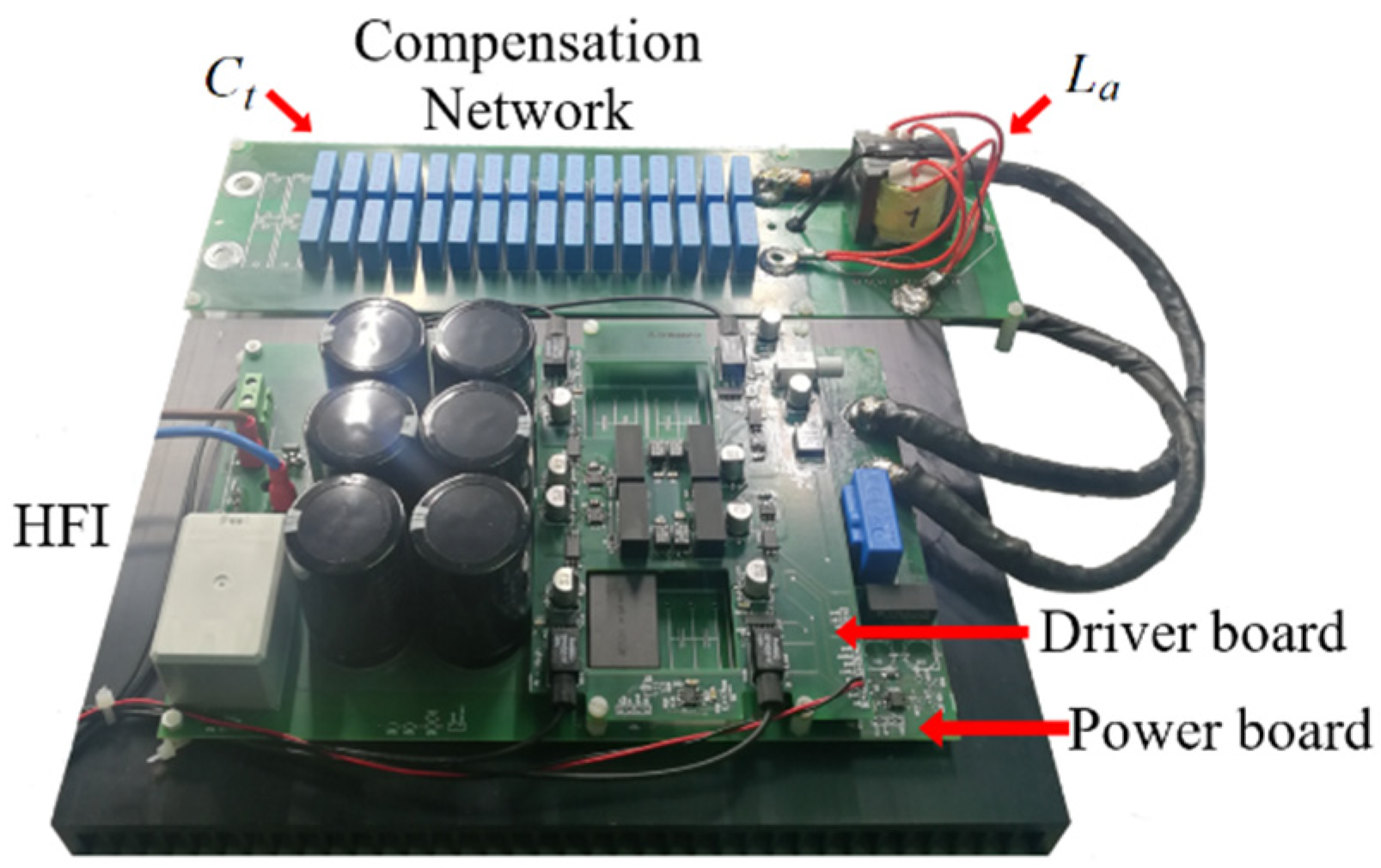
One of the HFIs and the compensation network of the relevant track coil are reported in
Figure 13. The three HFIs are composed of a power board and a driver board and share a single electronic control unit (ECU) implemented by means of the DSP TMS320F28335 from Texas Instruments (Dallas, TX, USA) [
31]. The DSP executes the control algorithm and generates the gate commands that are forwarded to the HFIs by means of an optic fiber connection. This solution allows the DSP to synchronize the PWM signals of all the HFI units and to monitor the detection of overcurrents by the HFIs protection circuitry. The ECUs of the HFIs and of the CH are endowed with the transceivers nRM24L01p manufactured by Nordic Semiconductor (Trondheim, Norway) [
32] used to established a radio-frequency connection by which the battery charging process is controlled and monitored.
In order to reduce the parasitic elements and the ringing during the switching, a compact design based on a four layers PCB layout has been developed for the HFIs. It led to an improvement of the conversion efficiency and avoided the failure of the power switches; to these aims the selection of the power switches is crucial, because their parasitic parameters could cause a degradation of the performance as well as their own fault.
For the implementation of the HFIs power stage, MDmesh MOSFET transistors with part number STW65N65DM2AG produced by STMicroelectronics (Geneva, Switzerland) have been selected because of their fast-recovery body diode and very low parasitic capacitances. Insulation of the gate commands has been performed by means of the Silicon Labs Si826x devices while the gates themselves are driven by the Microchip MIC4452 (Chandler, AZ, USA) driver, supplied by the isolated dc/dc power supply Tracopower TEC 3-1213W (Zurich, Switzerland). Each HFI is endowed with a dc-link overcurrent protection implemented by comparing the voltage across a shunt resistor with a threshold value by means of a STMicroelectronics STLM311 voltage comparator. The comparator output signal is latched with a D-type flip-flop and then used to disable the gates command coming from the optic fiber.
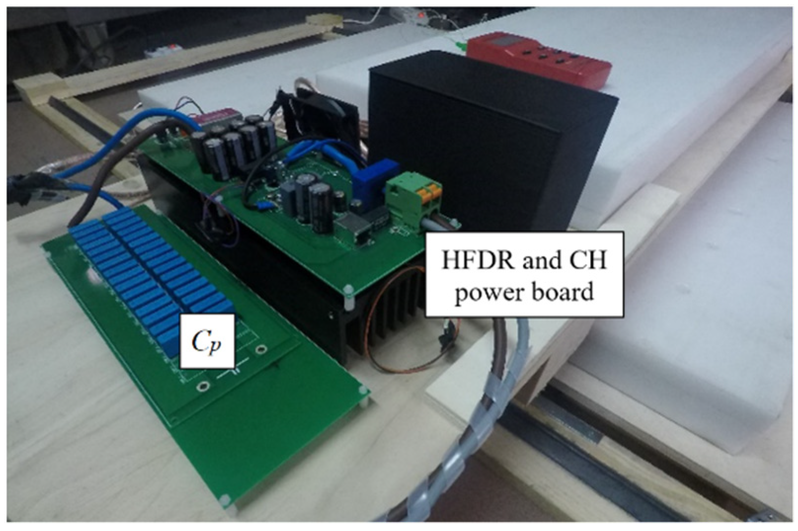
The HFDR and the CH have been built on a single power board, as shown in
Figure 14. The HFDR is made of four ultra-fast diode STTH61W04S produced by STMicroelectronics [
33] while for the CH the power MOSFET IXTK120N65X2 from IXYS (Milpitas, CA, USA) [
34] and the freewheeling diode STTH200W06TV1 from STMicroelectronics [
35] have been used.
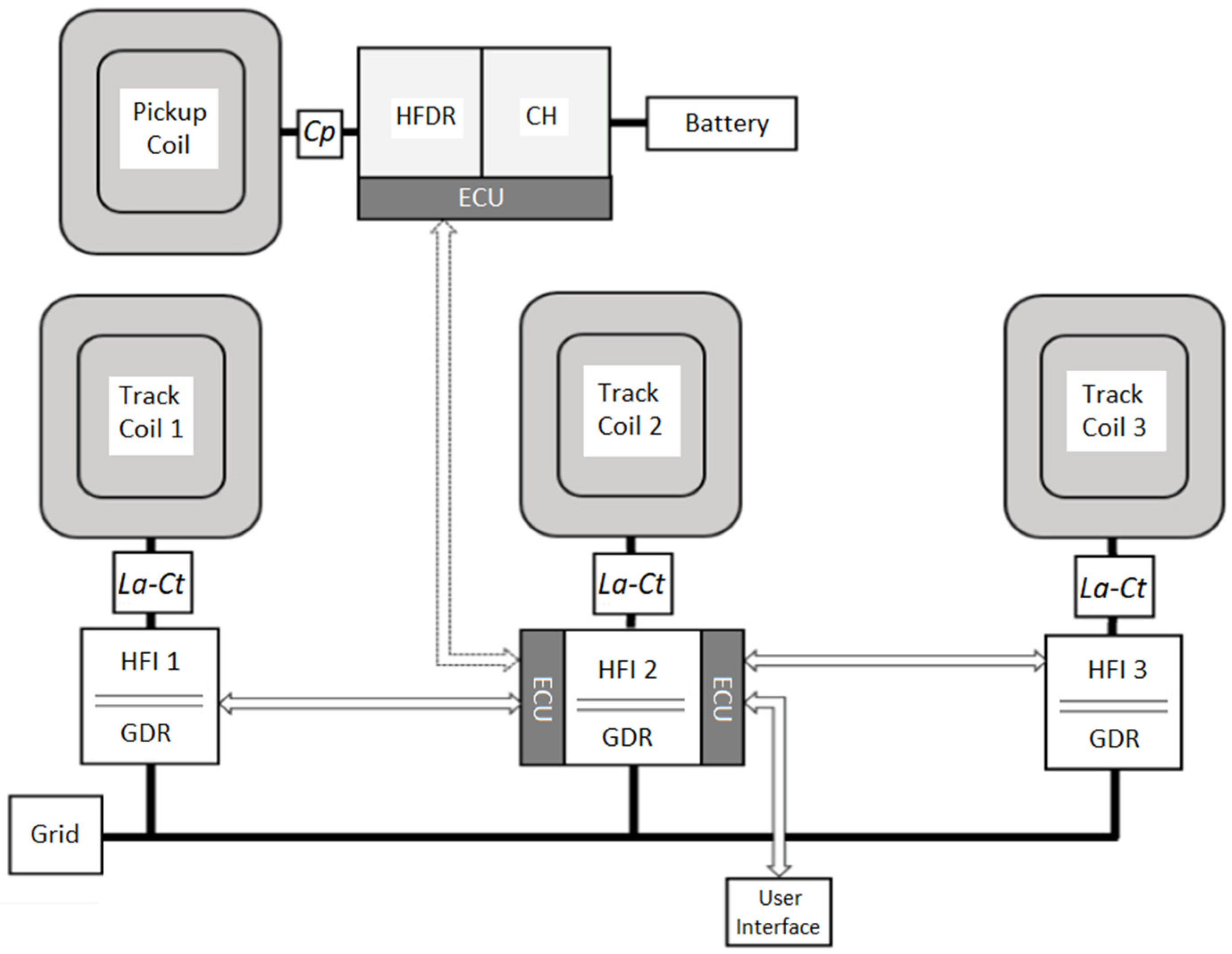
The pickup ECU is based on the DSP TMS320F28335 and its main tasks are the implementation of the charging algorithm of the battery and the management of the communication with the HFIs control unit. The overall layout of the WPT system is sketched in
Figure 15.
6. Experimental Results
To validate the performance of the prototypal WPT system, a number of tests have been performed on the laboratory set-up. During the tests, each HFI generates a square wave voltage with the same amplitude and phase of those generated by the other two HFIs. The trolley with the pickup is pulled at constant speed of about 10 km/h along the rails, from a starting position on the left of the first track coil to a final position on the right of the third one; in the first test the pickup is centered over the track coils and the airgap between them is fixed to 100 mm. In order to speed up the test execution and to make easier the data acquisition, an electronic load CHROMA 63804 (TestEquity, Moorpark, CA, USA) has been used during the tests instead of the vehicle battery pack.
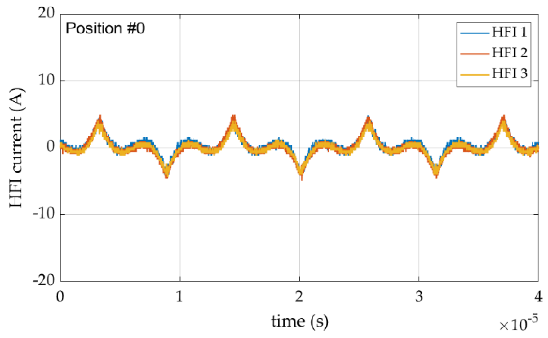
Figure 16 is relevant to Position #0; here the pickup is not coupled with any of the track coils, thus no power is transferred to the pickup power stage unit. The three currents generated by the HFIs exhibit the peculiar waveforms characteristic of the LCL compensation n in not-coupled condition: their first harmonic components are small and shifted of π/2 with respect to the supply voltages so that no active power is supplied by the HFIs besides the losses in coils windings and in the cores. According to the system design, the three currents are perfectly in-phase.
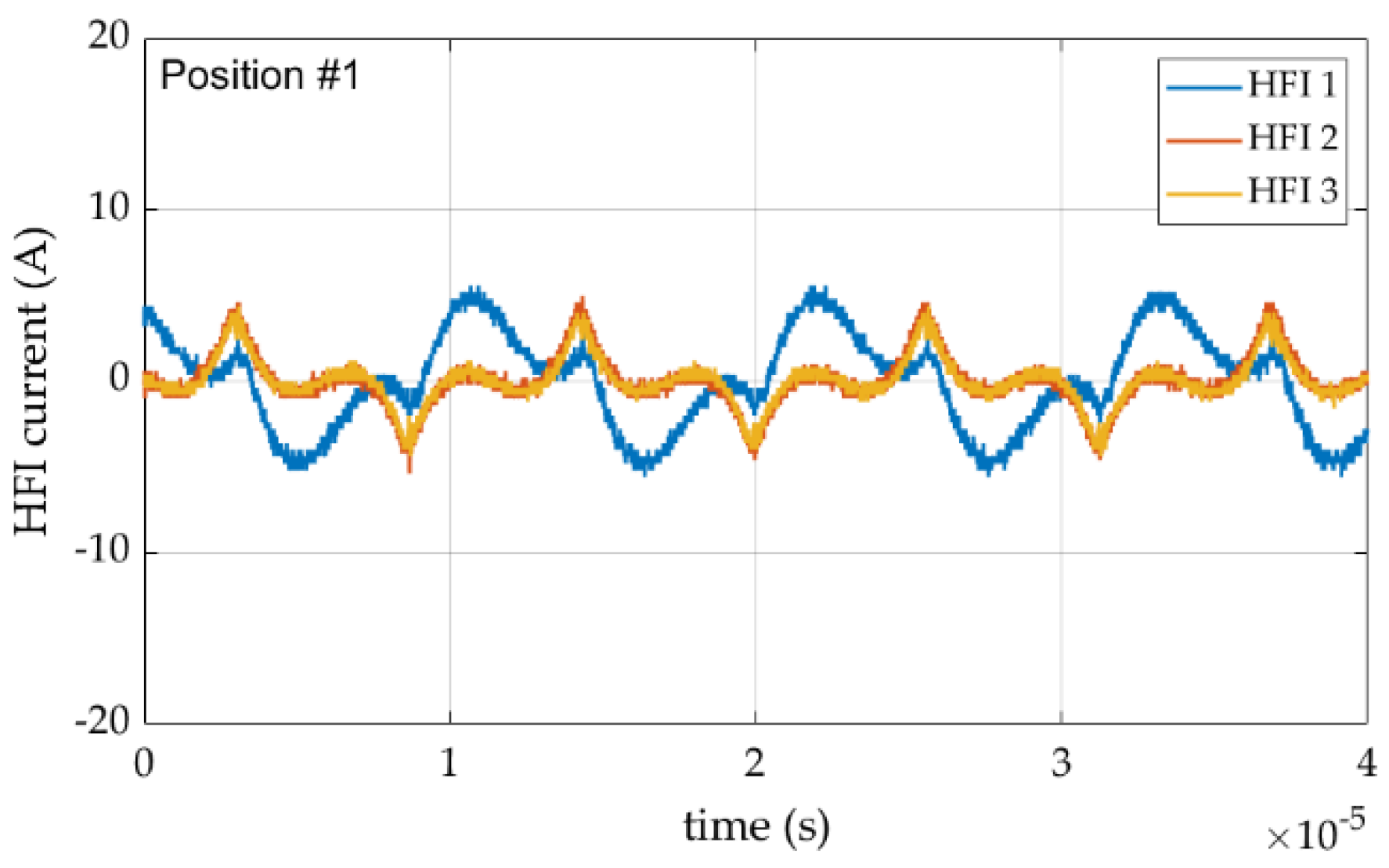
Figure 17 reports the currents waveforms relevant to the Position #1, where the pickup is half-coupled with the first track coil but not coupled with any of the other two. The current supplied by the first HFI, plotted with the blue line, now has a higher first harmonic component shifted about π/2 ahead with respect to the other two currents and is in phase with the relevant supply voltage. In this condition the power transferred to the pickup is half of the rated one and is supplied only by the first HFI while the currents at the output of the other two maintain the same waveforms reported in the previous figure and do not contribute to the transferred power.
Figure 18 shows the waveforms of the currents when the pickup is in Position #2, fully coupled with the first of the track coils but not with the others. In this condition, the current in the coupled track coil reaches its maximum amplitude and is nearly sinusoidal, as expected, while the waveforms of the other two currents still maintain the waveforms shown in
Figure 16 and
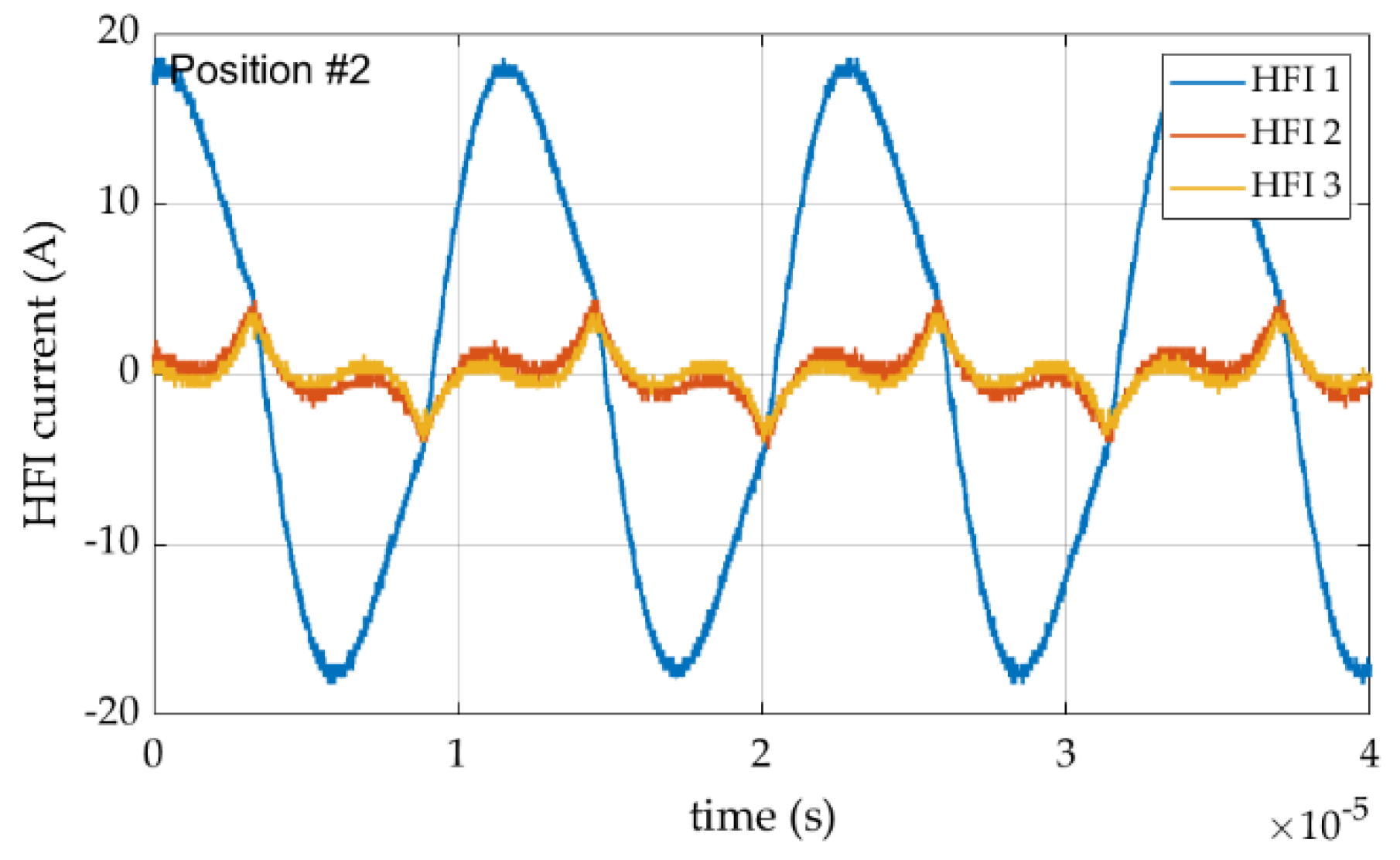
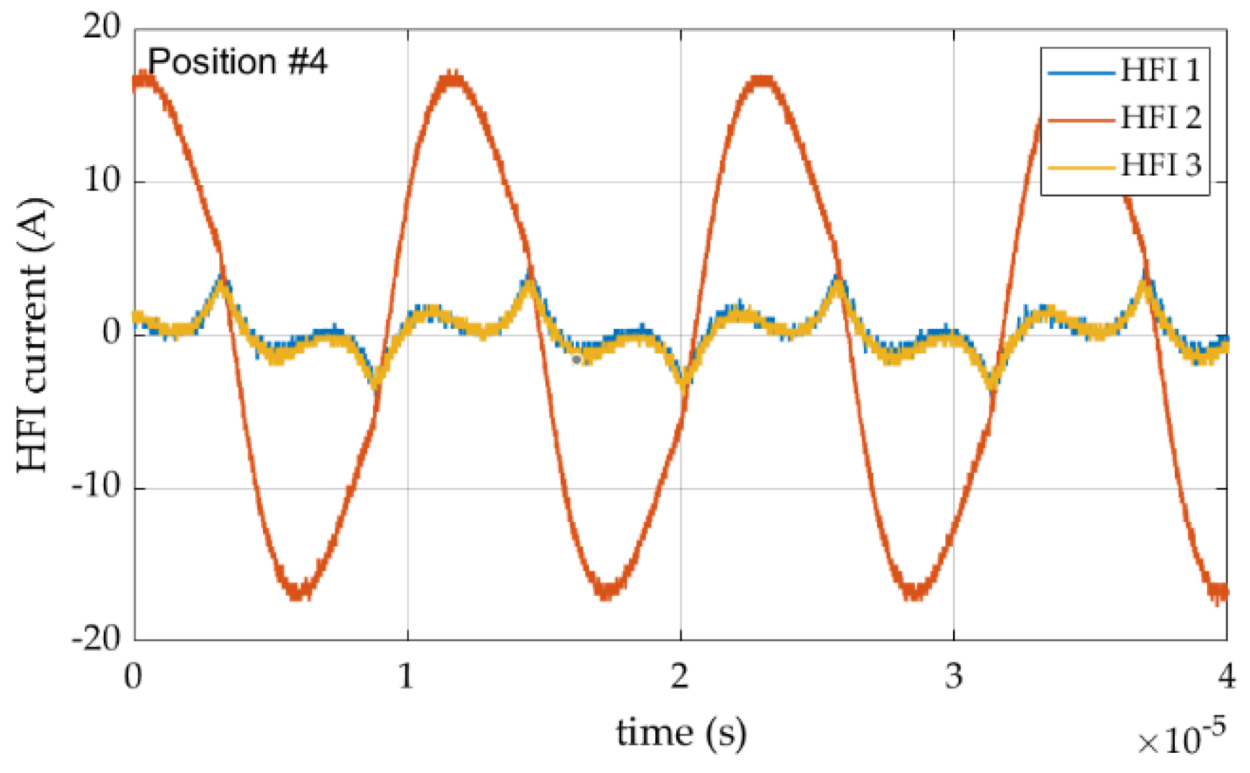
Figure 17. The power transferred to the pickup is now about equal to the nominal one.
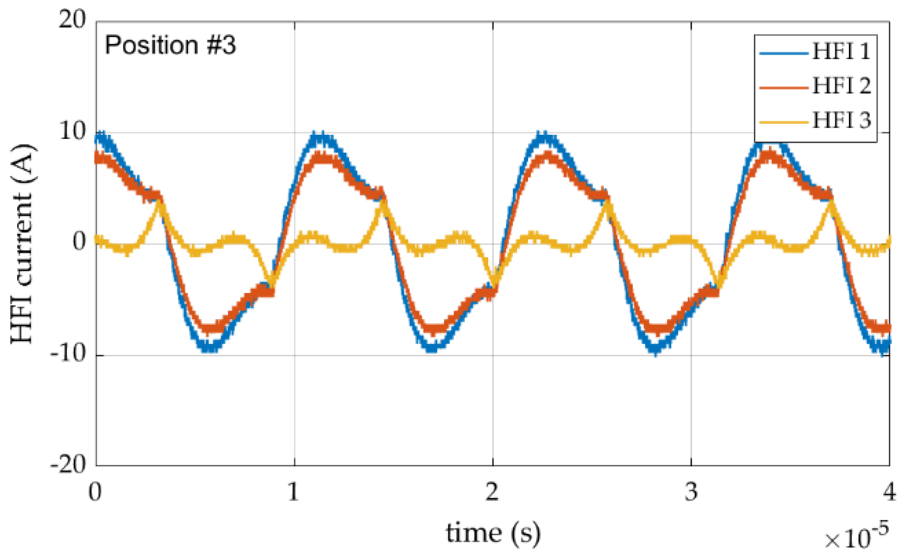
Figure 19 refers to position #3, with the pickup laying between the first and the second track coil. As expected, in this position both the currents in the track coils have sensible first harmonic components; the latter ones have the same phase, both lead of π/2 the third current, and cooperate in transferring power to the pickup. Being the pickup nearly in the middle between the two track coils, the amplitudes of the two currents are almost equal.
The currents relevant to the subsequent Position #4 are shown in
Figure 20. Here the current of the second HFI increases and reaches the maximum amplitude with a waveform similar to that plotted in
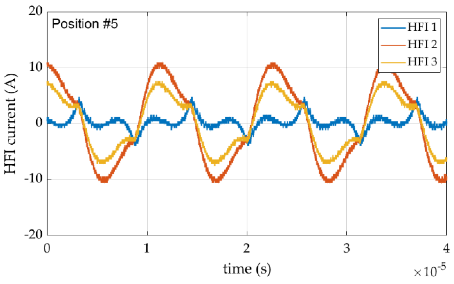
Figure 17 while the other two currents decrease in amplitude and take again the waveform typical of the not coupled condition. In Position# 5 the pickup is about in the middle between the second and the third track coil and the waveforms of the currents of the second and the third HFI, reported in
Figure 21, are similar to those of
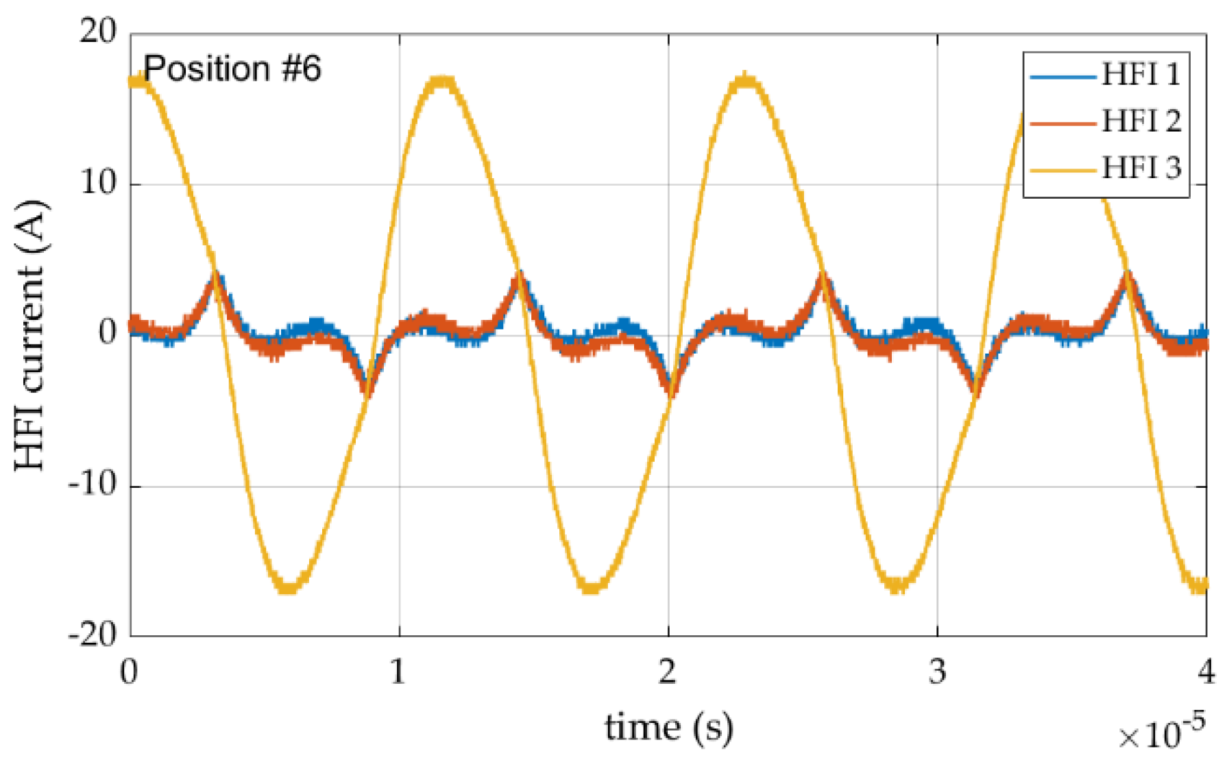
Figure 18. In Position# 6, the pickup is aligned with the third track coil and the current of the third HFI, plotted in
Figure 22, increases to its maximum amplitude like the current of the first HFI in
Figure 18 and that of the second one in
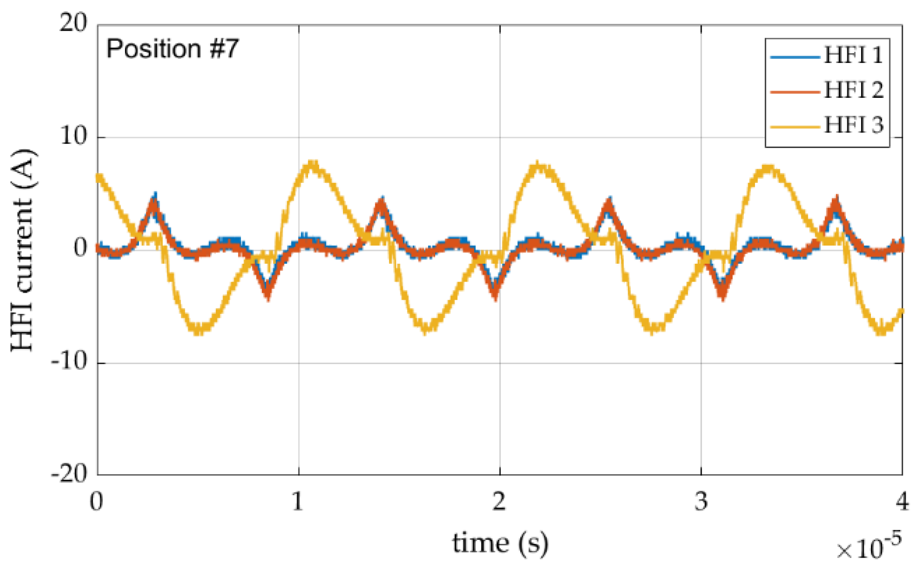
Figure 20. In Position #7 the pickup is leaving the third track coil and the current of the relevant HFI, shown in
Figure 23, is similar to that plotted in
Figure 18 and
Figure 20.
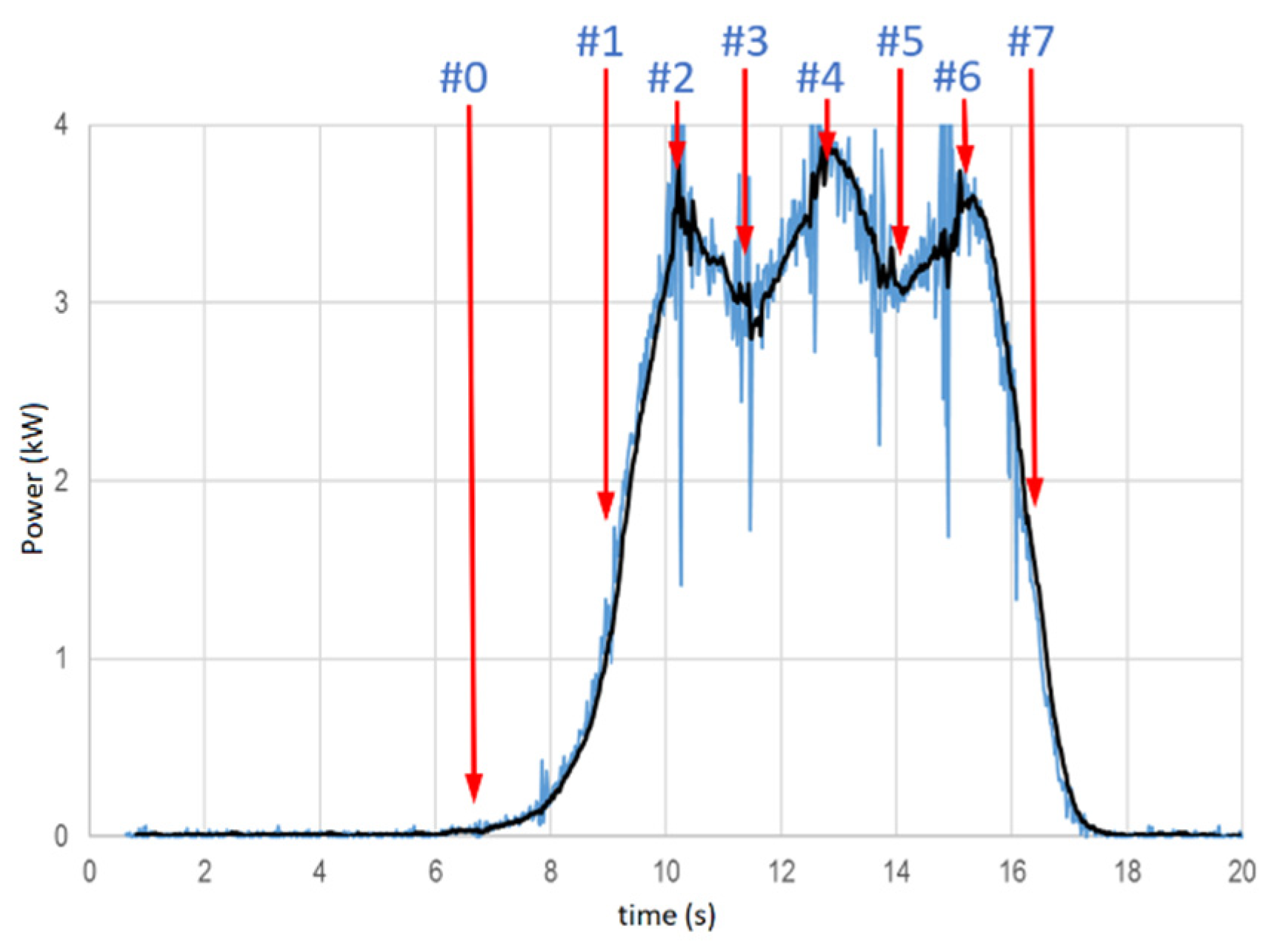
The profile of the power transferred to the electronic load while the pickup moves along the track is plotted in
Figure 24. The positions considered in the previous discussion are highlighted by red arrows. The figure shows that the transferred power reaches its maxima when the pickup is aligned with one track coil. When the pickup lays between two track coils the system is less effective in supplying the load and, despite the joint contributions from two track coils, the transferred power falls down to its minima. In any case, the average transferred power from Position#2 to Position#6 fulfills the requirement set in
Section 2, being about equal to 3.2 kW.
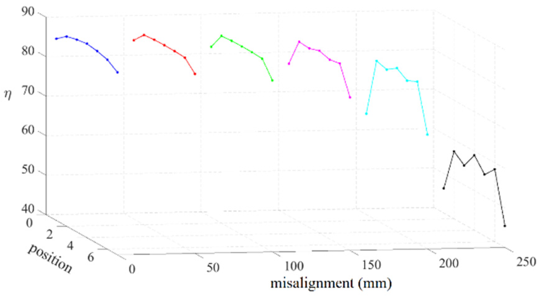
The overall power transfer efficiency, measured as the ratio between the active power delivered to the electronic load and that absorbed from the grid, is a function of the pickup position with respect to the track coils. The plots of the efficiency obtained at different pickup positions along the track and different values of misalignment are reported in
Figure 25. The blue curve on the left refers to the pickup moving on the center of the track coils, in the same positions that gave rise to the currents waveforms and the power profile reported in
Figure 16,
Figure 17,
Figure 18,
Figure 19,
Figure 20,
Figure 21,
Figure 22 and
Figure 23. This shows that the overall efficiency is always higher than 85% and that, in contrast to the transferred power, it does not exhibit any variation while the pickup moves between two track coils. The next curves on the right refer to the same pickup positions along the track but with increasing misalignment. Up to the fourth magenta curve, relevant to a misalignment of 150 mm, the efficiency is not heavily affected by the misalignment and maintains a flat behavior in the central positions even its values at Position #1 and Position #7 decrease. With misalignments higher than 150 mm the efficiency decreases more and more and becomes more sensitive to the position of the pickup when it moves between two coils. With a misalignment of 250 mm, corresponding to the rightmost black curve, only half of each sub-coil of the pickup is faced to the corresponding sub-coil of the track coil, nevertheless the efficiency is still higher than 55% along most of the pickup travel.
7. Conclusions
The paper presented a comprehensive procedure for the design, the manufacturing, and the test of a dynamic WPT system for an electric city-car. The power requirements of the vehicle and the dimensional constraints for the installation of the receiving coil have been at first defined. From them, the sizing of the power converter and of the coupling set has been derived and their design has been carried out. Details about the building of the coils and of the converters are given together with indications about the component used in the prototype. Finally, the results of a number of tests performed on the prototype are reported to confirm the soundness of the design procedure.
Author Contributions
Conceptualization, M.B. and G.B.; methodology, M.B., M.D.M., and G.T.; software, M.D.M.; validation, M.D.M. and G.T.; formal analysis, M.B.; investigation, M.B. and G.B.; resources, A.G.; data curation, M.D.M. and G.T.; writing-original draft preparation, M.B.; writing-review and editing, M.B., G.B., and M.D.M.; visualization, M.B. and M.D.M.; supervision, A.G.; project administration, A.G.; funding acquisition, A.G. All authors have read and agreed to the published version of the manuscript.
Funding
This work has been supported by ENEA (Italian National Agency for New Technologies, Energy and Sustainable Economic Development) within the project no. RdS/PAR2017/209 entitled “Studio e progetto preliminare per un sistema di ricarica dinamica wireless”.
Conflicts of Interest
The authors declare no conflict of interest.
References
- Kindl, V.; Frivaldsky, M.; Zavrel, M.; Pavelek, M. Generalized Design Approach on Industrial Wireless Chargers. Energies 2020, 13, 2697. [Google Scholar] [CrossRef]
- Zhou, Y.; Liu, C.; Huang, Y. Wireless Power Transfer for Implanted Medical Application: A Review. Energies 2020, 13, 2837. [Google Scholar] [CrossRef]
- La Rosa, R.; Livreri, P.; Trigona, C.; Di Donato, L.; Sorbello, G. Strategies and Techniques for Powering Wireless Sensor Nodes through Energy Harvesting and Wireless Power Transfer. Sensors 2019, 19, 2660. [Google Scholar] [CrossRef] [Green Version]
- Ludowicz, W.; Pietrowski, W.; Wojciechowski, R.M. Analysis of an Operating State of the Innovative Capacitive Power Transmission System with Sliding Receiver Supplied by the Class-E Inverter. Electronics 2020, 9, 841. [Google Scholar] [CrossRef]
- Wen, F.; Cheng, X.; Li, Q.; Ye, J. Wireless Charging System Using Resonant Inductor in Class E Power Amplifier for Electronics and Sensors. Sensors 2020, 20, 2801. [Google Scholar] [CrossRef]
- Skouras, T.A.; Gkonis, P.K.; Ilias, C.N.; Trakadas, P.T.; Tsampasis, E.G.; Zahariadis, T.V. Electrical Vehicles: Current State of the Art, Future Challenges, and Perspectives. Clean Technol. 2020, 2, 1. [Google Scholar] [CrossRef] [Green Version]
- Bi, Z.; Kan, T.; Mi, C. A review of wireless power transfer for electric vehicles: Prospects to enhance sustainable mobility. Appl. Energy 2016, 179, 413–425. [Google Scholar] [CrossRef] [Green Version]
- Nguyen, M.T.; Nguyen, C.V.; Truong, L.H.; Le, A.M.; Quyen, T.V.; Masaracchia, A.; Teague, K.A. Electromagnetic Field Based WPT Technologies for UAVs: A Comprehensive Survey. Electronics 2020, 9, 461. [Google Scholar] [CrossRef] [Green Version]
- Abou Houran, M.; Yang, X.; Chen, W. Magnetically Coupled Resonance WPT: Review of Compensation Topologies, Resonator Structures with Misalignment, and EMI Diagnostics. Electronics 2018, 7, 296. [Google Scholar] [CrossRef] [Green Version]
- Buja, G.; Bertoluzzo, M.; Mude, K.N. Design and experimentation of WPT charger for electric city-car. IEEE Trans. Ind. Electron. 2015, 62, 7436–7447. [Google Scholar] [CrossRef]
- Luo, B.; Shou, Y.; Lu, J.; Li, M.; Deng, X.; Zhu, G. A Three-Bridge IPT System for Different Power Levels Conversion under CC/CV Transmission Mode. Electronics 2019, 8, 884. [Google Scholar] [CrossRef] [Green Version]
- Laporte, S.; Coquery, G.; Deniau, V.; De Bernardinis, A.; Hautière, N. Dynamic Wireless Power Transfer Charging Infrastructure for Future EVs: From Experimental Track to Real Circulated Roads Demonstrations. World Electr. Veh. J. 2019, 10, 84. [Google Scholar] [CrossRef] [Green Version]
- Marmiroli, B.; Dotelli, G.; Spessa, E. Life Cycle Assessment of an On-Road Dynamic Charging Infrastructure. Appl. Sci. 2019, 9, 3117. [Google Scholar] [CrossRef] [Green Version]
- Buja, G.; Bertoluzzo, M.; Dashora, H.K. Lumped track layout design for dynamic wireless charging of electric vehicles. IEEE Trans. Ind. Electron. 2016, 63, 6631–6640. [Google Scholar] [CrossRef]
- De Marco, D.; Dolara, A.; Longo, M.; Yaïci, W. Design and Performance Analysis of Pads for Dynamic Wireless Charging of EVs using the Finite Element Method. Energies 2019, 12, 4139. [Google Scholar] [CrossRef] [Green Version]
- Yang, S.-C.; He, H.; Yan, X.-Y.; Chen, Y.-H.; Hua, Y.; Cao, Y.-G.; Li, J.; Li, H.-H.; Yin, S. Segmental Track Analysis in Dynamic Wireless Power Transfer. Energies 2019, 12, 3875. [Google Scholar] [CrossRef] [Green Version]
- Wen, F.; Chu, X.; Li, Q.; Gu, W. Compensation Parameters Optimization of Wireless Power Transfer for Electric Vehicles. Electronics 2020, 9, 789. [Google Scholar] [CrossRef]
- Urbe, Veicoli da Città. Available online: http://webtv.enea.it/immagini-a-caso/urbe-veicoli-da-citta/view (accessed on 17 June 2020).
- JWireless Power Transfer for Light-Duty Plug-In/Electric Vehicles and Alignment Methodology; SAE International: Warrendale, PA, USA, 2019; p. J2954.
- Dashora, H.K.; Buja, G.; Bertoluzzo, M.; Pinto, R.; Lopresto, V. Analysis and design of DD coupler for dynamic wireless charging of electric vehicles. J. Electromagn. Waves Appl. 2018, 32, 170–189. [Google Scholar] [CrossRef]
- Zhang, W.; White, J.C.; Abraham, A.M.; Mi, C.C. Loosely Coupled Transformer Structure and Interoperability Study for EV Wireless Charging Systems. IEEE Trans. Power Electron. 2015, 30, 6356–6367. [Google Scholar] [CrossRef]
- Budhia, M.; Boys, J.T.; Covic, G.A.; Huang, C.-Y. Development of a single-sided flux magnetic coupler for electric vehicle IPT charging systems. IEEE Trans. Ind. Electron. 2013, 60, 318–328. [Google Scholar] [CrossRef]
- Seong, J.Y.; Lee, S.-S. Optimization of the Alignment Method for an Electric Vehicle Magnetic Field Wireless Power Transfer System Using a Low-Frequency Ferrite Rod Antenna. Energies 2019, 12, 4689. [Google Scholar] [CrossRef] [Green Version]
- McDonough, M.; Fahimi, B. A study on the effects of motion in inductively coupled vehicular charging applications. In Proceedings of the IEEE Transportation Electrification Conference Expo (ITEC), Dearborn, MI, USA, 18 June 2012; pp. 1–5. [Google Scholar]
- Bertoluzzo, M.; Buja, G.; Dashora, H.K. Design of DWC system track with unequal DD coil set. IEEE Trans. Transp. Electrif. 2017, 3, 380–391. [Google Scholar] [CrossRef]
- Tampubolon, M.; Pamungkas, L.; Chiu, H.-J.; Liu, Y.-C.; Hsieh, Y.-C. Dynamic Wireless Power Transfer for Logistic Robots. Energies 2018, 11, 527. [Google Scholar] [CrossRef] [Green Version]
- Jha, R.K.; Buja, G.; Bertoluzzo, M.; Giacomuzzi, S.; Mude, K.N. Performance comparison of the one-element resonant EV wireless battery chargers. IEEE Trans. Ind. Appl. 2018, 54, 2471–2482. [Google Scholar] [CrossRef]
- Gati, E.; Kokosis, S.; Patsourakis, N.; Manias, S. Comparison of Series Compensation Topologies for Inductive Chargers of Biomedical Implantable Devices. Electronics 2020, 9, 8. [Google Scholar] [CrossRef] [Green Version]
- Huang, C.Y.; Boys, J.T.; Covic, G.A. Resonant network design considerations for variable coupling lumped coil systems. In Proceedings of the IEEE Energy Conversions Congress Expo, Raleigh, NC, USA, 15 September 2012; pp. 3841–3847. [Google Scholar]
- Wang, Y.; Lin, F.; Yang, Z.; Liu, Z. Analysis of the Influence of Compensation Capacitance Errors of a Wireless Power Transfer System with SS Topology. Energies 2017, 10, 2177. [Google Scholar] [CrossRef] [Green Version]
- TMS320F2833x, TMS320F2823x Digital Signal Controllers (DSCs). Available online: http://www.ti.com/lit/ds/symlink/tms320f28335.pdf (accessed on 17 February 2020).
- Nordic Semiconductor. Available online: https://www.nordicsemi.com/Products/Low-power-short-range-wireless/nRF24-series (accessed on 17 February 2020).
- STTH61W04S Turbo 2 Ultrafast High Voltage Rectifier. Available online: https://www.st.com/resource/en/datasheet/stth61w04s.pdf (accessed on 17 February 2020).
- X2-Class Power MOSFET. Available online: https://m.littelfuse.com/~/media/electronics/datasheets/discrete_mosfets/littelfuse_discrete_mosfets_n-channel_ultra_junction_ixt_120n65x2_datasheet.pdf.pdf (accessed on 17 February 2020).
- Turbo 2 Ultrafast High Voltage Rectifier. Available online: https://4donline.ihs.com/images/VipMasterIC/IC/SGST/SGSTS35936/SGSTS35936-1.pdf?hkey=52A5661711E402568146F3353EA87419 (accessed on 17 February 2020).
Figure 1.
Picture of the case study electric vehicle (EV) Urbe.
Figure 1.
Picture of the case study electric vehicle (EV) Urbe.
Figure 2.
Double D (DD) coupling set.
Figure 2.
Double D (DD) coupling set.
Figure 3.
Coil layout of the wireless power transfer (WPT) system.
Figure 3.
Coil layout of the wireless power transfer (WPT) system.
Figure 4.
Mutual inductance profiles.
Figure 4.
Mutual inductance profiles.
Figure 5.
Pickup side conversion stage schematic.
Figure 5.
Pickup side conversion stage schematic.
Figure 6.
Track side conversion stage schematic.
Figure 6.
Track side conversion stage schematic.
Figure 7.
Circuital scheme of the track coil with inductive capacitive inductive (LCL) compensation.
Figure 7.
Circuital scheme of the track coil with inductive capacitive inductive (LCL) compensation.
Figure 8.
Pickup side conversion stage schematic.
Figure 8.
Pickup side conversion stage schematic.
Figure 9.
Alternate component of ir,out.
Figure 9.
Alternate component of ir,out.
Figure 10.
DD coil layout.
Figure 10.
DD coil layout.
Figure 11.
Layout of the experimental track.
Figure 11.
Layout of the experimental track.
Figure 12.
Experimental coil layout.
Figure 12.
Experimental coil layout.
Figure 13.
High-frequency inverter (HFI) and compensation network of a track coil.
Figure 13.
High-frequency inverter (HFI) and compensation network of a track coil.
Figure 14.
High frequency diode rectifier (HFDR), chopper (CH), and compensation network of the pickup coil.
Figure 14.
High frequency diode rectifier (HFDR), chopper (CH), and compensation network of the pickup coil.
Figure 15.
Layout of the WPT system.
Figure 15.
Layout of the WPT system.
Figure 16.
HFIs output currents in not-coupled condition (Position #0).
Figure 16.
HFIs output currents in not-coupled condition (Position #0).
Figure 17.
HFIs output currents with partial coupling with the first track coil (Position #1).
Figure 17.
HFIs output currents with partial coupling with the first track coil (Position #1).
Figure 18.
HFIs output currents with full coupling with the first track coil (Position #2).
Figure 18.
HFIs output currents with full coupling with the first track coil (Position #2).
Figure 19.
HFIs output currents with partial coupling with the first and the second track coils (Position #3).
Figure 19.
HFIs output currents with partial coupling with the first and the second track coils (Position #3).
Figure 20.
HFIs output currents with full coupling with the second track coil (Position #4).
Figure 20.
HFIs output currents with full coupling with the second track coil (Position #4).
Figure 21.
HFIs output currents with partial coupling with the second and the third track coils (Position #5).
Figure 21.
HFIs output currents with partial coupling with the second and the third track coils (Position #5).
Figure 22.
HFIs output currents with full coupling with the third track coil (Position #6).
Figure 22.
HFIs output currents with full coupling with the third track coil (Position #6).
Figure 23.
HFIs output currents with partial coupling with the third track coil (Position #7).
Figure 23.
HFIs output currents with partial coupling with the third track coil (Position #7).
Figure 24.
Power transferred to the battery in different pickup positions.
Figure 24.
Power transferred to the battery in different pickup positions.
Figure 25.
Power transfer efficiency vs pickup misalignment.
Figure 25.
Power transfer efficiency vs pickup misalignment.
Table 1.
Urbe data.
| Quantity | Symbol | Value |
|---|
| Mass | m | 756 kg |
| Maximum speed | Umax | 50 km/h |
| Aerodynamic friction coefficient | Cd | 0.28 |
| Frontal area | Af | 2.1 m2 |
| Revolving friction coefficient | Krf | 0.01 |
| Traction drive efficiency | ηtd | 0.82 |
| Maximum pickup width | bmax | 1.150 m |
| Maximum pickup length | lmax | 1.450 m |
| Ground clearance | Gc | 0.1 m |
| Battery nominal voltage | Vb,N | 48 V |
| Battery maximum voltage | Vb,max | 56 V |
| Battery minimum voltage | Vb,min | 36 V |
| Maximum battery charging power | Pb,max | 670 W |
Table 2.
Coupling set characteristics.
Table 2.
Coupling set characteristics.
| Quantity | Symbol | Value |
|---|
| Length | l | 0.335 m |
| Width | b | 0.95 m |
| Number of turns | nt | 4 |
| Number of bars | nb | 6 |
| Mutual inductance | M0 | 14 μH |
| Self-inductance | Lt, Lp | 54 μH |
| Coupling coefficient | k | 0.26 |
| Pickup current | | 78.8 A |
| Track coil current | | 11.7 A |
| Pickup voltage | | 2424 V |
| Track coil voltage | | 750 V |
Table 3.
Positions of the pickup with respect to the track coils.
Table 3.
Positions of the pickup with respect to the track coils.
| Pickup Position | x (mm) |
|---|
| Position #0 | −450 |
| Position #1 | −210 |
| Position #2 | 0 |
| Position #3 | 225 |
| Position #4 | 445 |
| Position #5 | 645 |
| Position #6 | 895 |
| Position #7 | 1065 |
© 2020 by the authors. Licensee MDPI, Basel, Switzerland. This article is an open access article distributed under the terms and conditions of the Creative Commons Attribution (CC BY) license (http://creativecommons.org/licenses/by/4.0/).

 ,
, 


