Design and Evaluation of Cell Interaction Based Vedic Multiplier Using Quantum-Dot Cellular Automata


Abstract
:1. Introduction
2. Related Works
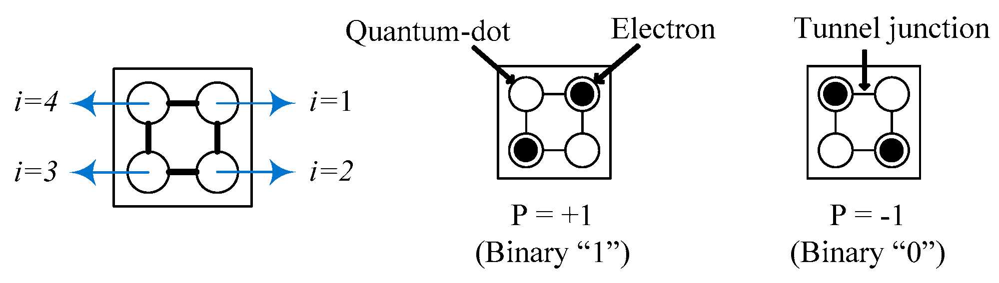
2.1. Basic QCA
M(A,B,1) = A + B
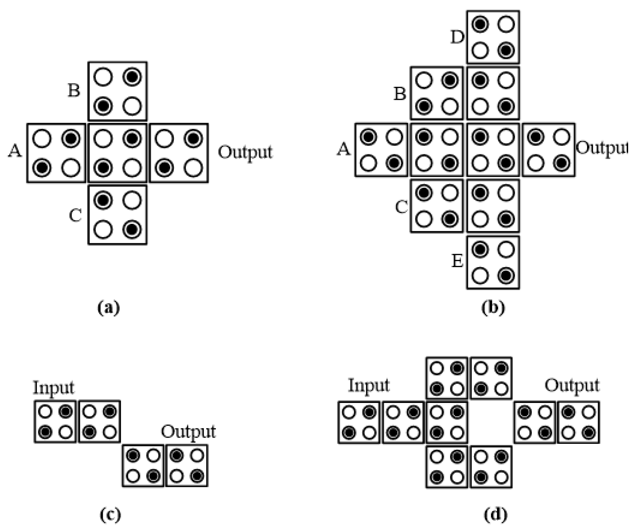
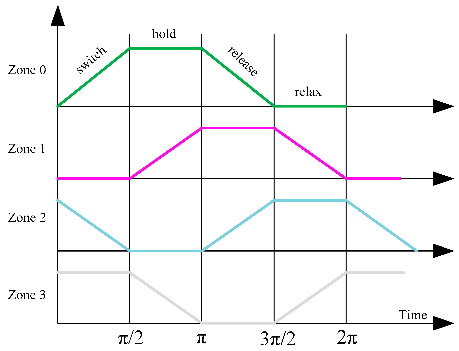
2.2. QCA Clocking
2.3. Wire Crossing in QCA
3. The Proposed Structures
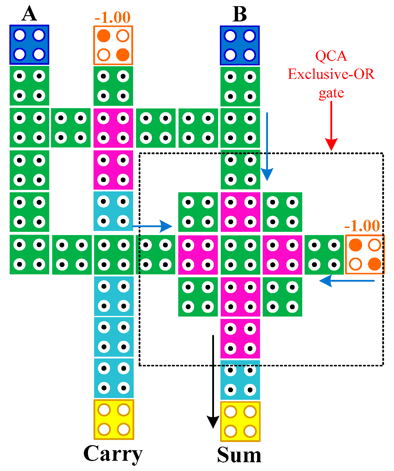
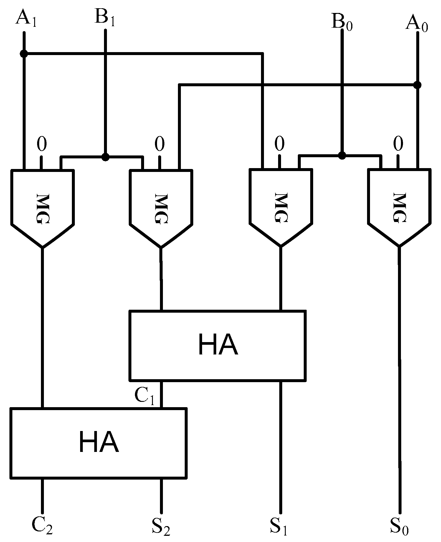
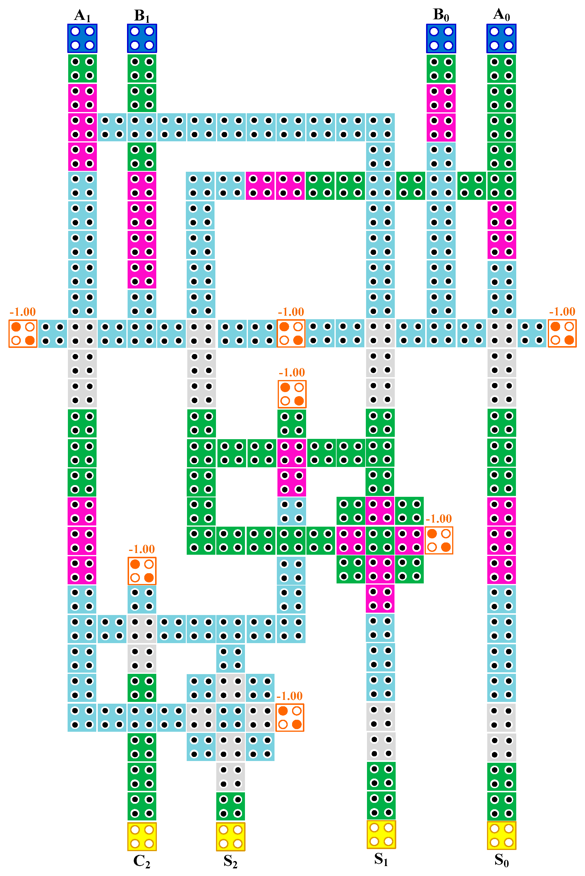
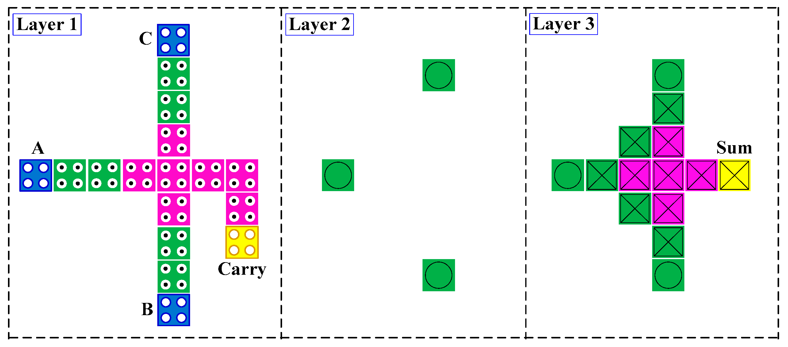
3.1. Half Adder for the Multiplier
Carry out = M(A,B,0)
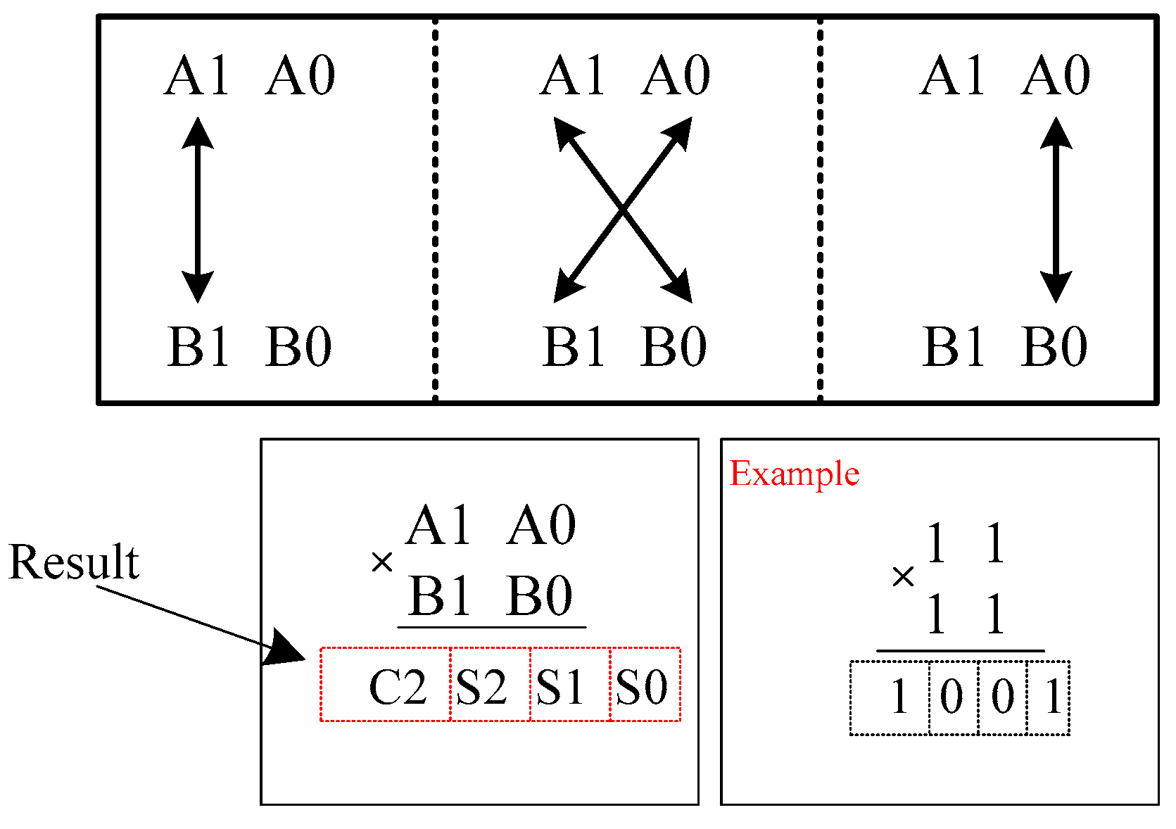
3.2. The 2 × 2 Bit Vedic Multiplier
- The coefficient of x2 indicates the vertical multiplication of a and c.
- The coefficient of x expresses cross-wise multiplication of a with d and b with c, along with the addition of both outputs.
- The constant is the vertical multiplication of b and d.
C1S1 = A1B0 + A0B1
C2S2 = C1 + A1B1
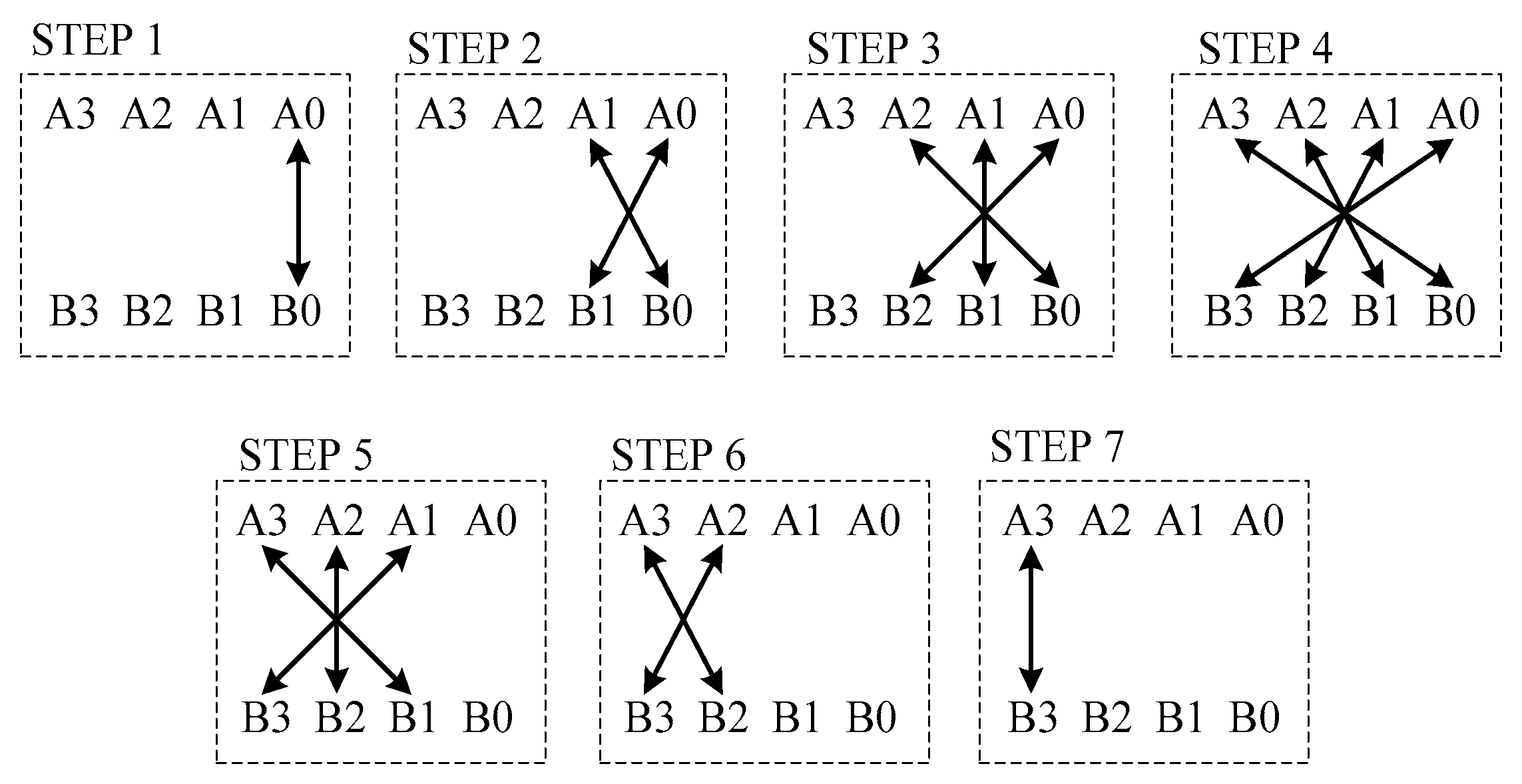
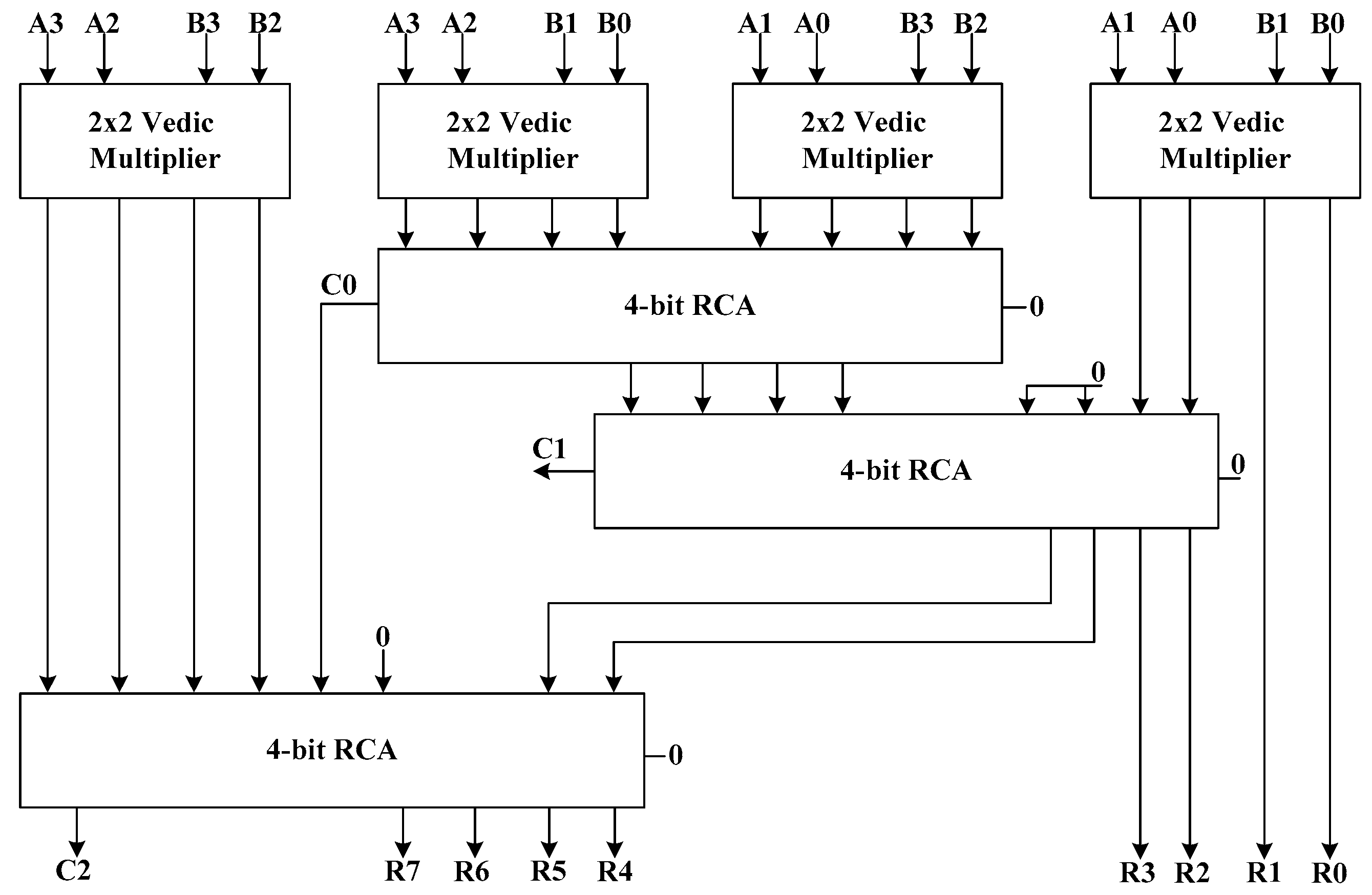
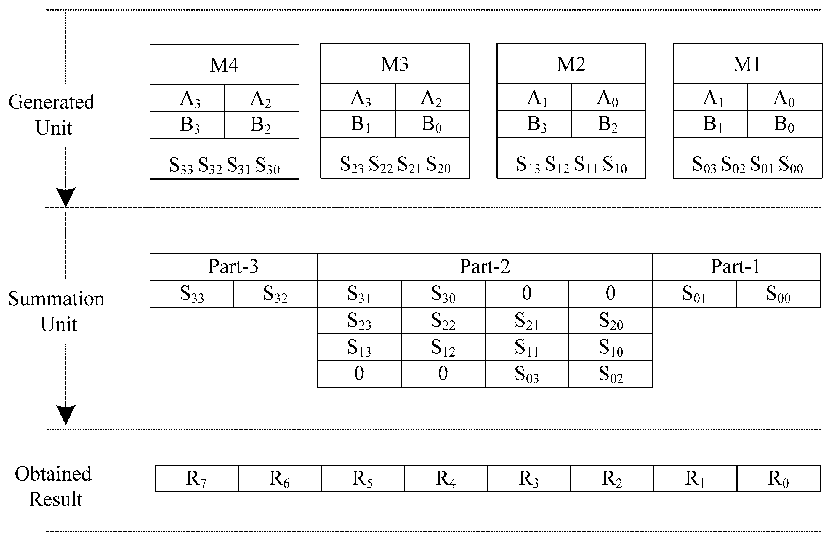
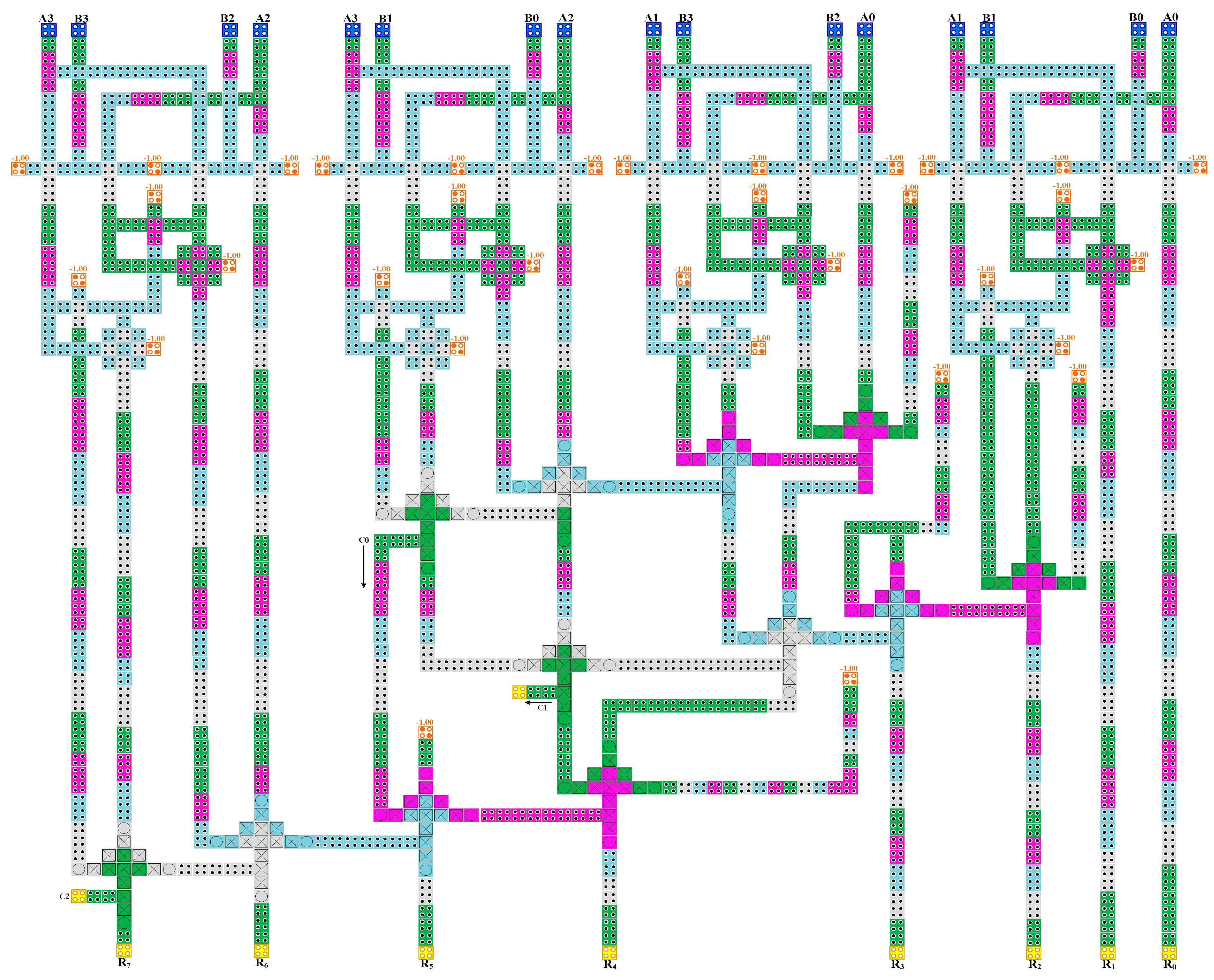
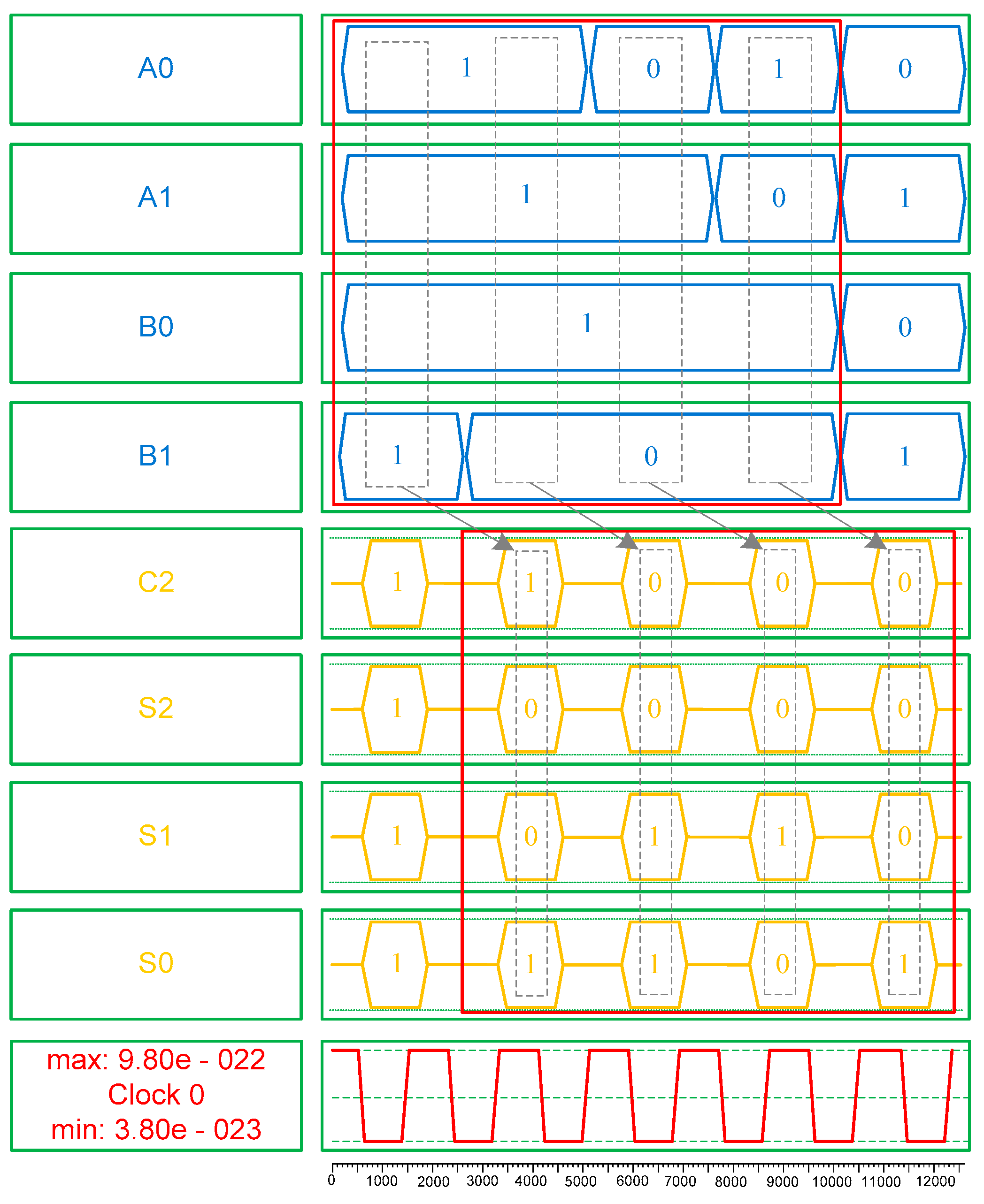
3.3. The 4 × 4 Bit Vedic Multiplier
C1S1 = A1B0 + A0B1
C2S2 = C1 + A0 B2 + A2 B0 + A1 B1
C3S3 = C2 + A0 B3 + A3 B0 + A1B2 + A2B1
C4S4 = C3 + A1B3 + A3B1 + A2B2
C5S5 = C4 + A3B2 + A2B3
C6S6 = C5 + A3B3
4. Simulation Results and Analyses
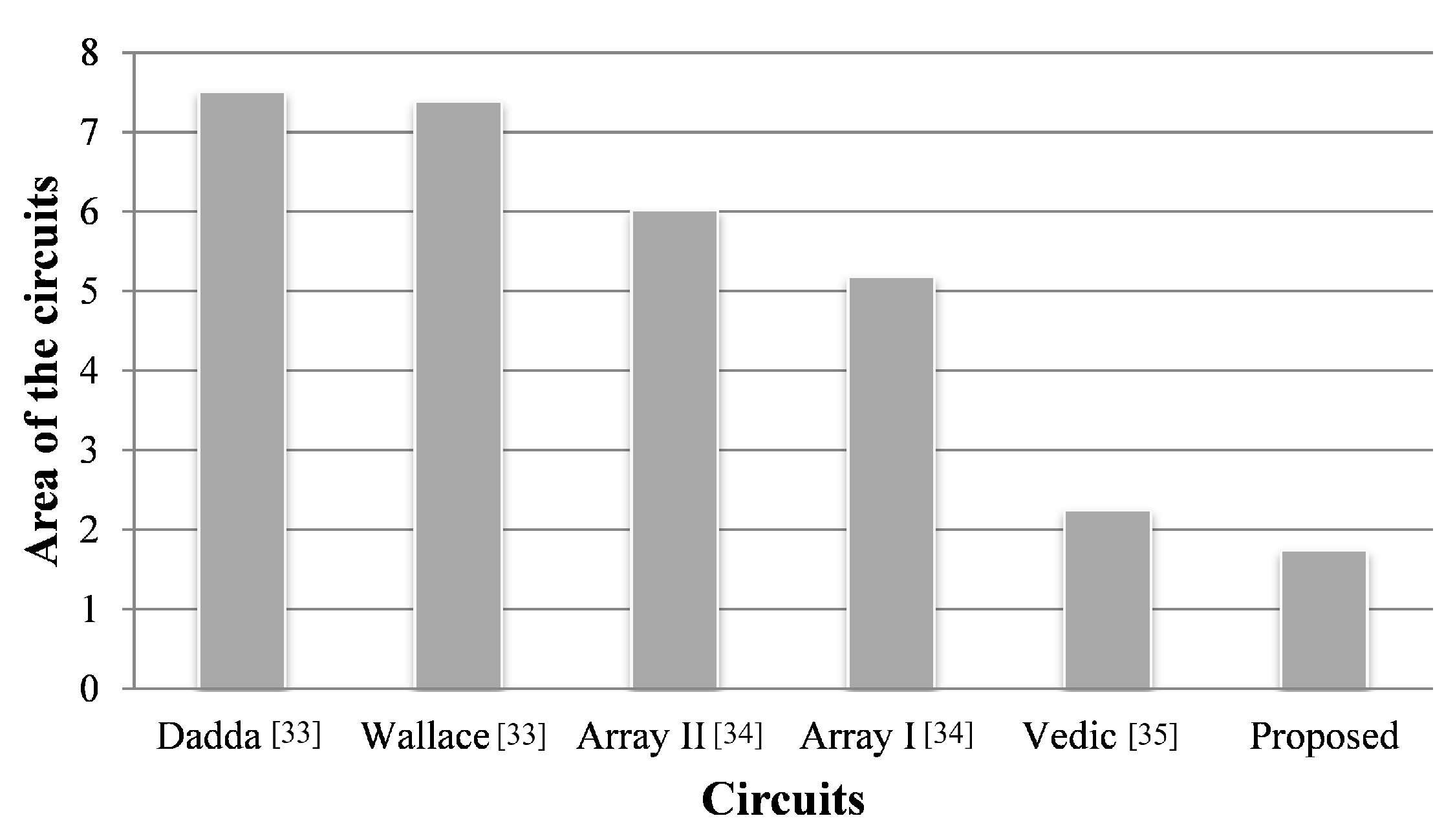
4.1. Structural Analysis
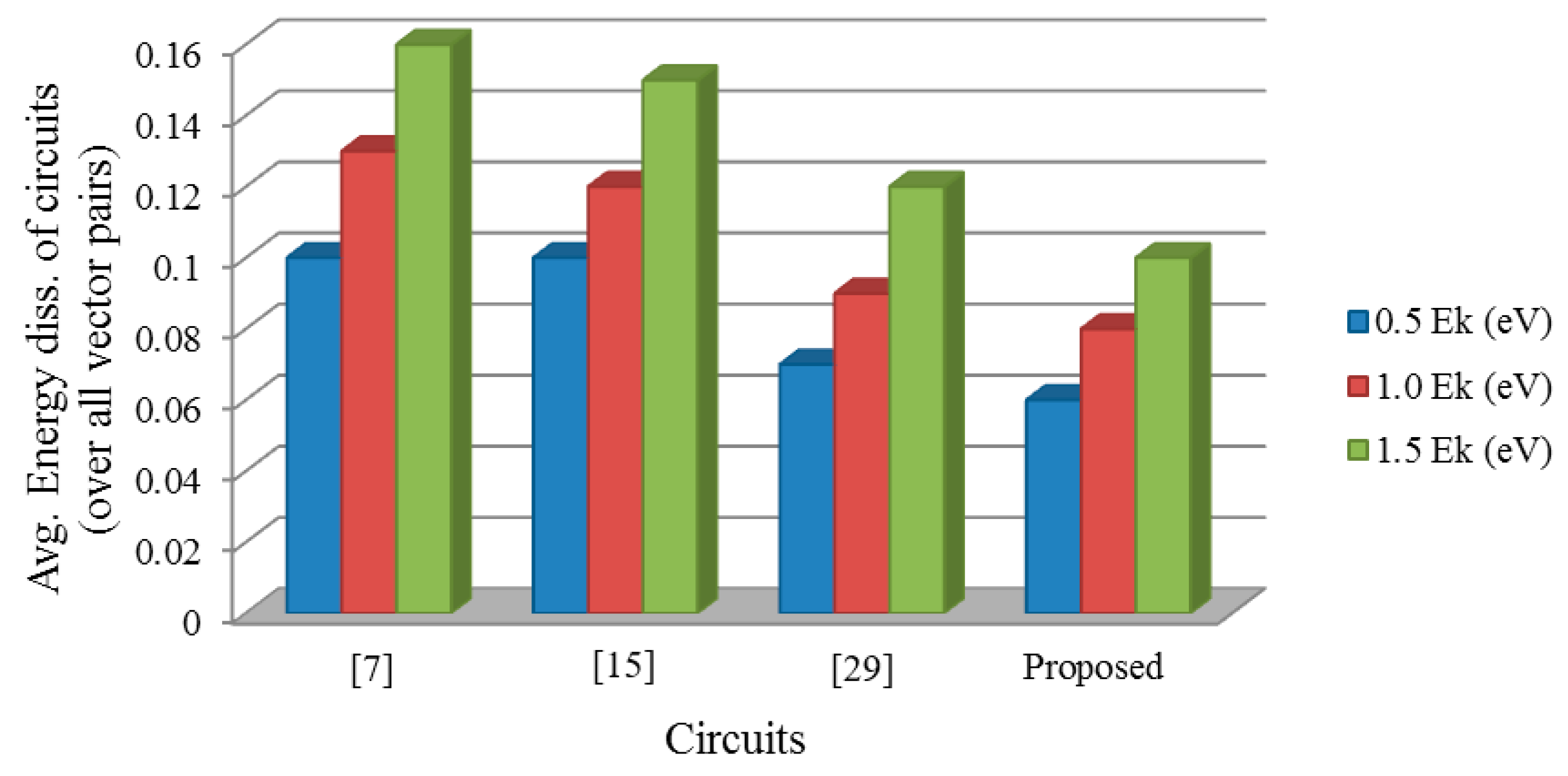
4.2. Energy Dissipation Analysis
5. Conclusions
Author Contributions
Funding
Conflicts of Interest
References
- Lent, C.S.; Tougaw, P.D.; Porod, W.; Bernstein, G.H. Quantum cellular automata. Nanotechnology 1993, 4, 49–57. [Google Scholar] [CrossRef]
- Jeon, J.C. Five-Input Majority Gate Based QCA Decoder. Adv. Sci. Technol. Lett. 2016, 122, 95–99. [Google Scholar]
- Safoev, N.; Jeon, J.C. A novel controllable inverter and adder/subtractor in quantum-dot cellular automata using cell interaction based XOR gate. Microelectron. Eng. 2020, 222, 111197. [Google Scholar] [CrossRef]
- Safoev, N.; Jeon, J.C. Design of high-performance QCA incrementer/decrementer circuit based on adder/subtractor methodology. Microprocess. Microsyst. 2020, 72, 102927. [Google Scholar] [CrossRef]
- Lent, C.S.; Snider, G.L. The development of quantum-dot cellular automata. In Field-Coupled Nanocomputing; Springer: Berlin/Heidelberg, Germany, 2014; Volume 8280, pp. 3–20. [Google Scholar]
- You, Y.W.; Jeon, J.C. Two Dimensional QCA XOR Logic Using NNI Gate. Int. J. Control Autom. 2017, 10, 217–226. [Google Scholar] [CrossRef]
- Cho, H.; Swartzlander, E.E. Adder designs and analyses for quantum-dot cellular automata. IEEE Trans. Nanotechnol. 2007, 6, 374–383. [Google Scholar] [CrossRef]
- Jeon, J.C. Low Complexity QCA Universal Shift Register Design Using Multiplexer and D Flip-Flop Based on Electronic Correlations. J. Supercomput. 2019, 1–15. [Google Scholar] [CrossRef]
- Erniyazov, S.; Jeon, J.C. Carry save adder and carry look ahead adder using inverter chain based coplanar QCA full adder for low energy dissipation. Microelectron. Eng. 2019, 211, 37–43. [Google Scholar] [CrossRef]
- Jeon, J.C. Extendable Quantum-dot Cellular Automata Decoding Architecture Using 5-input Majority Gate. Int. J. Control Autom. 2015, 8, 107–118. [Google Scholar] [CrossRef]
- Safoev, N.; Jeon, J.C. Low area complexity demultiplexer based on multilayer Quantum-dot Cellular Automata. Int. J. Control Autom. 2016, 9, 165–178. [Google Scholar] [CrossRef]
- Safoev, N.; Jeon, J.C. Peres Gate Realization in QCA for Reversible Binary Incrementer. Adv. Sci. Lett. 2017, 23, 9812–9817. [Google Scholar] [CrossRef]
- DiLabio, G.A.; Wolkow, R.A.; Pitters, J.L.; Piva, P.G. Atomistic Quantum Dots. U.S. Patent Application No. 8,816,479, 26 August 2014. [Google Scholar]
- Tiwari, H.D.; Gankhuyag, G.; Kim, C.M. Multiplier design based on ancient Indian Vedic Mathematics. In Proceedings of the 2008 International SoC Design Conference: (ISOCC), Busan, Korea, 24–25 November 2008. [Google Scholar]
- Chudasama, A.; Sasamal, T.N.; Yadav, J. An efficient design of Vedic multiplier using ripple carry adder in Quantum-dot Cellular Automata. Comput. Electr. Eng. 2017, 65, 527–542. [Google Scholar] [CrossRef]
- Thapliyal, H.; Arabnia, H.R. A Time-Area-Power Efficient Multiplier and Square Architecture Based on Ancient Indian Vedic Mathematics. In Proceedings of the International Conference on VLSI (VLSI ‘04), Las Vegas, NV, USA, 21–24 June 2004; pp. 434–439. [Google Scholar]
- Safoev, N.; Jeon, J.C. QCA XOR gate for Arithmetic and Logic Circuit Design. In Proceedings of the IIER International Conference, Tokyo, Japan, 25–28 September 2017. [Google Scholar]
- Ahmadpour, S.S.; Mosleh, M. New Designs of Fault-tolerant adders in Quantum-Dot Cellular Automata. Nano Commun. Netw. 2019, 19, 10–25. [Google Scholar] [CrossRef]
- Kalogeiton, V.S.; Papadopoulos, D.P.; Liolis, O.; Mardiris, V.A.; Sirakoulis, G.C.; Karafyllidis, I.G. Programmable Crossbar Quantum-Dot Cellular Automata Circuits. IEEE Trans. Comp. Int. Syst. 2016, 36, 1367–1380. [Google Scholar] [CrossRef] [Green Version]
- Lu, L.; Liu, W.; O’Neill, M.; Swartzlander, E.E. QCA systolic array design. IEEE Trans. Comput. 2013, 62, 548–560. [Google Scholar] [CrossRef]
- Sasamal, T.N.; Singh, A.K.; Mohan, A. An optimal design of full adder based on 5-input majority gate in coplanar quantum-dot cellular automata. Optik 2016, 127, 8576–8591. [Google Scholar] [CrossRef]
- Vankamamidi, V.; Ottavi, M.; Lombardi, F. Two-Dimensional Schemes for Clocking/Timing of QCA Circuits. IEEE Trans. Comput. Aided Des. Integr. Circuits Syst. 2008, 27, 34–44. [Google Scholar] [CrossRef]
- Das, J.C.; De, D. Circuit Switching with Quantum-Dot Cellular Automata. Nano Commun. Netw. 2017, 14, 16–28. [Google Scholar] [CrossRef]
- Lent, C.S.; Liu, M.; Lu, Y. Bennett Clocking of Quantum-Dot Cellular Automata and the Limits to Binary Logic Scaling. Nanotechnology 2006, 17, 4240–4251. [Google Scholar] [CrossRef] [Green Version]
- Farazkish, R.; Khodaparast, F. Design and characterization of a new fault-tolerant full-adder for quantum-dot cellular automata. Microprocess. Microsyst. 2015, 39, 426–433. [Google Scholar] [CrossRef]
- Jeon, J.C. Designing nanotechnology QCA-multiplexer using majority function-based NAND for quantum computing. J. Supercomput. 2020. [Google Scholar] [CrossRef]
- You, Y.W.; Jeon, J.C. Multilayered Design of Clocked SR Flip-Flop Using Quantum-Dot Cellular Automata. Adv. Sci. Lett. 2017, 23, 9835–9840. [Google Scholar] [CrossRef]
- Safoev, N.; Jeon, J.C. Cell Interaction Based QCA Multiplexer for Complex Circuit Design. J. Comput. Theor. Nanosci. 2017, 23, 10097–10101. [Google Scholar] [CrossRef]
- Balali, M.; Rezai, A.; Balali, H.; Rabiei, F.; Emadi, S. Towards coplanar quantum-dot cellular automata adders based on efficient three-input XOR gate. Results Phys. 2017, 7, 1389–1395. [Google Scholar] [CrossRef]
- Ahmad, F.; Bhat, G.M.; Khademolhosseini, H.; Azimi, S.; Angizi, S.; Navi, K. Towards single layer quantum-dot cellular automata adders based on explicit interaction of cells. J. Comput. Sci. 2016, 16, 8–15. [Google Scholar] [CrossRef]
- Safoev, N.; Jeon, J.C. Compact RCA Based on Multilayer Quantum-dot Cellular Automata. In Information Systems Design and Intelligent Applications; Springer: Berlin/Heidelberg, Germany, 2018; pp. 515–524. [Google Scholar]
- Walus, K.; Dysart, T.J.; Jullien, G.A.; Budiman, R.A. QCADesigner: A Rapid Design and Simulation Tool for Quantum-Dot Cellular Automata. IEEE Trans. Nanotechnol. 2004, 3, 26–31. [Google Scholar] [CrossRef]
- Kim, S.W. Design of Parallel Multipliers and Dividers in QCA. UT Electronic Theses and Dissertations., University of Texas at Austin, Austin, TX, USA, May 2011. [Google Scholar]
- Kim, S.W.; Swartzlander, E.E. Parallel Multipliers for Quantum-Dot Cellular Automata. In Proceedings of the IEEE Nanotechnology Materialsand Devices Conference, Traverse City, MI, USA, 2–5 June 2009; pp. 68–72. [Google Scholar]
- Chudasama, A.; Sasamal, T.N. Implementation of 4x4 Vedic Multiplier using Carry Save Adder in Quantum-Dot Cellular Automata. In Proceedings of the 2016 International Conference on Communication and Signal Processing (ICCSP), Melmaruvathur, India, 6–8 April 2016; pp. 1260–1264. [Google Scholar]
- Srivastava, S.; Asthana, A.; Bhanja, S.; Sarkar, S. QCAPro-an error-power estimation tool for QCA circuit design. In Proceedings of the 14th IEEE International Symposium on Design and Diagnostics of Electronic Circuits and Systems, Cottbus, Germany, 13–15 April 2011; pp. 2377–2380. [Google Scholar]


| Input | Output | ||
|---|---|---|---|
| A | B | Sum | Carry |
| 0 | 0 | 0 | 0 |
| 0 | 1 | 1 | 0 |
| 1 | 0 | 1 | 0 |
| 1 | 1 | 0 | 1 |
| A1 | A0 | B1 | B0 | Output |
|---|---|---|---|---|
| 1 | 1 | 1 | 1 | 1001 |
| 1 | 1 | 0 | 1 | 0011 |
| 1 | 0 | 0 | 1 | 0010 |
| 0 | 1 | 0 | 1 | 0001 |
| Parameters | Bistable Approximation | Coherence Vector |
|---|---|---|
| Cell size | 18 nm | 18 nm |
| Dot diameter | 5 nm | 5 nm |
| Cell separation | 2 nm | 2 nm |
| Layer separation | 11.5 nm | 11.5 nm |
| Clock high | 9.8×10⁻²² J | 9.8×10⁻²² J |
| Clock low | 3.8×10⁻²³ J | 3.8×10⁻²³ J |
| Clock shift | 0 | 0 |
| Clock amplitude factor | 2.0 | 2.0 |
| Relative permittivity | 12.9 | 12.9 |
| Radius of effect | 65 nm | 80 nm |
| Circuit | Cell Count | Area | Delay | Cross-Over |
|---|---|---|---|---|
| 4 × 4Array I [33] | 2956 | 5.18 | 14 | Multilayer |
| 4 × 4Array II [33] | 3738 | 6.02 | 14 | Multilayer |
| 4 × 4 Dadda [34] | 3384 | 7.51 | 12 | Coplanar |
| 4 × 4 Wallace [34] | 3295 | 7.39 | 10 | Coplanar |
| 4 × 4 Vedic [35] | 1955 | 2.25 | 4.25 | Multilayer |
| 4 × 4 Proposed | 1726 | 1.74 | 5.25 | Multilayer |
| 2 × 2 Proposed | 194 | 0.17 | 2.25 | Coplanar |
| Designs | 0.5 Ek (eV) | 1.0 Ek (eV) | 1.5 Ek (eV) |
|---|---|---|---|
| [7] | 0.03 | 0.08 | 0.14 |
| [15] | 0.02 | 0.06 | 0.10 |
| [29] | 0.01 | 0.04 | 0.07 |
| Proposed | 0.01 | 0.03 | 0.06 |
© 2020 by the authors. Licensee MDPI, Basel, Switzerland. This article is an open access article distributed under the terms and conditions of the Creative Commons Attribution (CC BY) license (http://creativecommons.org/licenses/by/4.0/).
Share and Cite
Safoev, N.; Jeon, J.-C. Design and Evaluation of Cell Interaction Based Vedic Multiplier Using Quantum-Dot Cellular Automata. Electronics 2020, 9, 1036. https://doi.org/10.3390/electronics9061036
Safoev N, Jeon J-C. Design and Evaluation of Cell Interaction Based Vedic Multiplier Using Quantum-Dot Cellular Automata. Electronics. 2020; 9(6):1036. https://doi.org/10.3390/electronics9061036
Chicago/Turabian StyleSafoev, Nuriddin, and Jun-Cheol Jeon. 2020. "Design and Evaluation of Cell Interaction Based Vedic Multiplier Using Quantum-Dot Cellular Automata" Electronics 9, no. 6: 1036. https://doi.org/10.3390/electronics9061036