CMOS Analog AGC for Biomedical Applications

 , ,
, , 
Abstract
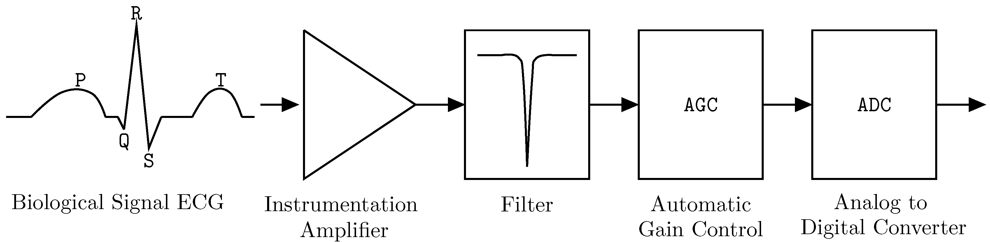
:1. Introduction
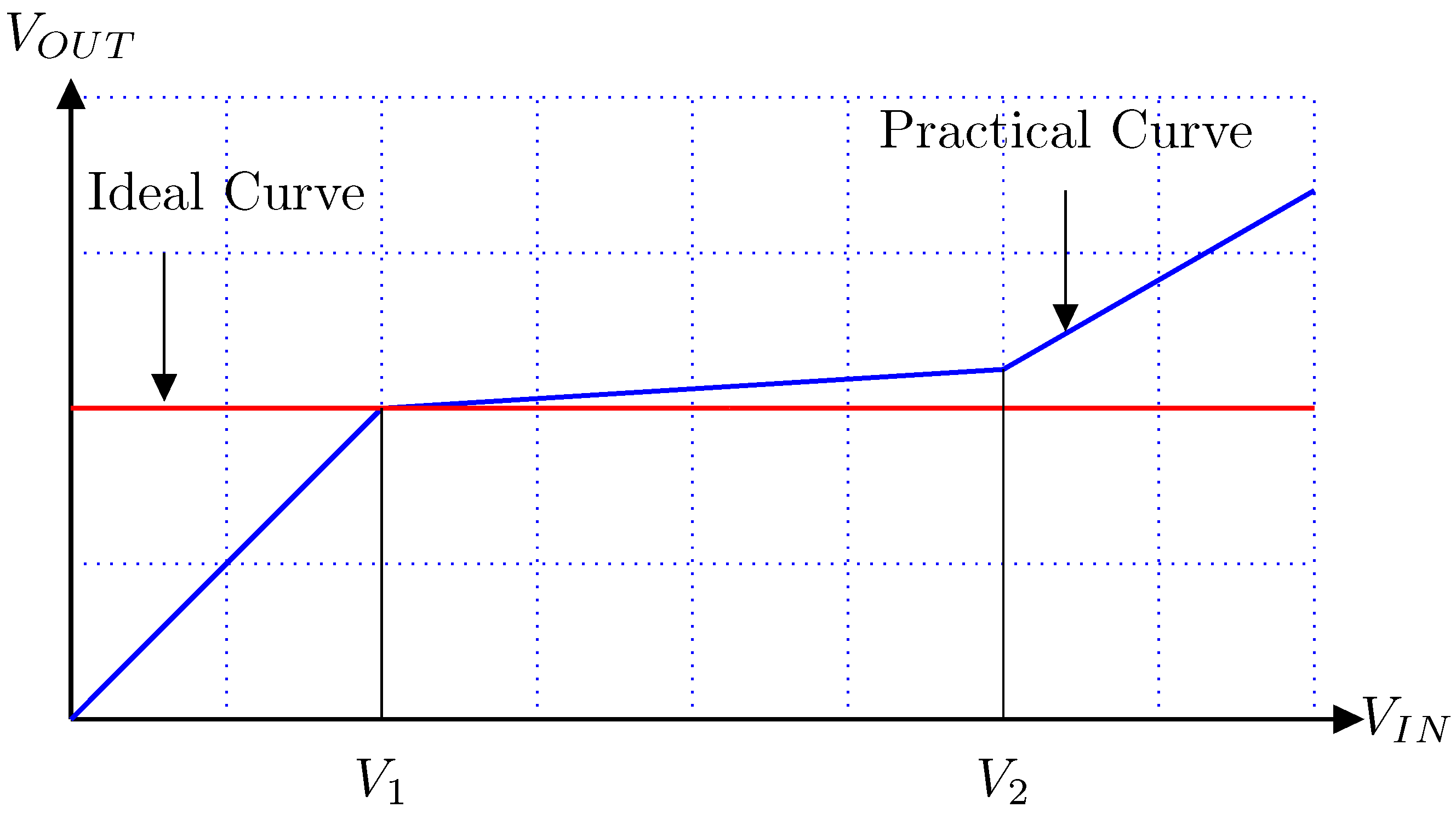
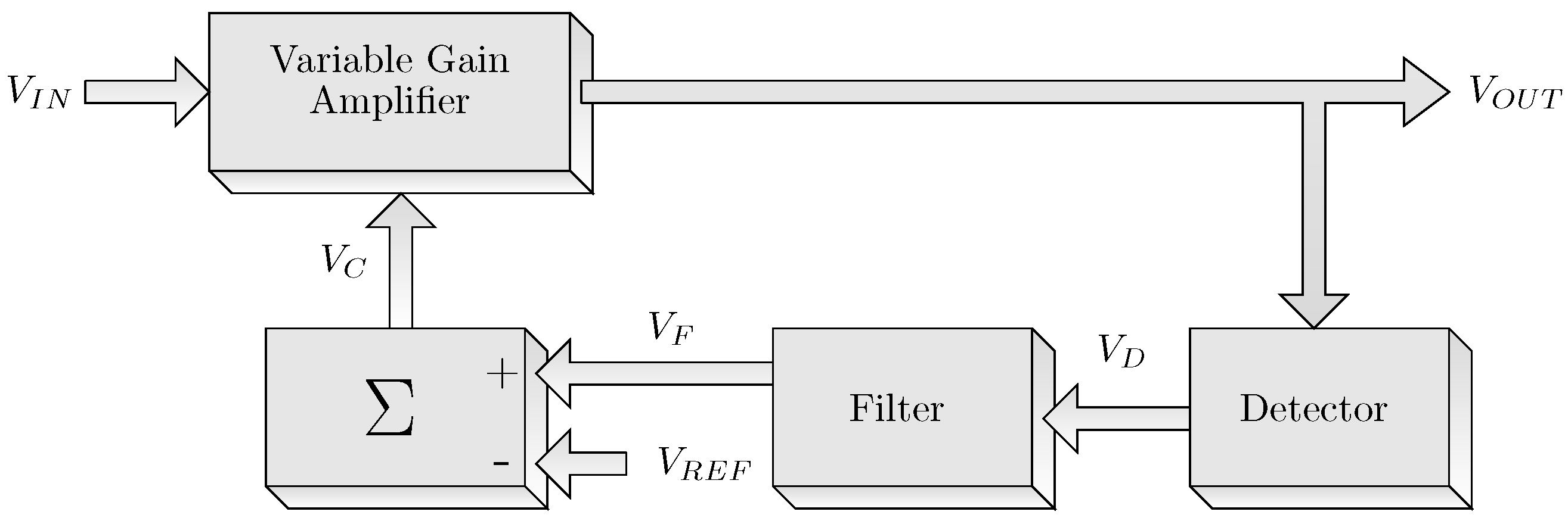
2. Automatic Gain Control (AGC)
- Settling time (): Set time needed by the circuit to regulate the loop gain in the AGC in response to a variation in amplitude in the input signal.
- Attack time (): Time necessary for the AGC to respond to an abrupt increase in the amplitude of the input signal. It is quantified from when the input signal changes until the AGC attenuates the output amplitude to a value close to the with a tolerance.
- Release time (): Time required for the AGC to respond to an abrupt loss in amplitude. It is quantified from when the input signal changes up until it amplifies the output signal to a value close to the with a tolerance.
Operating Principle
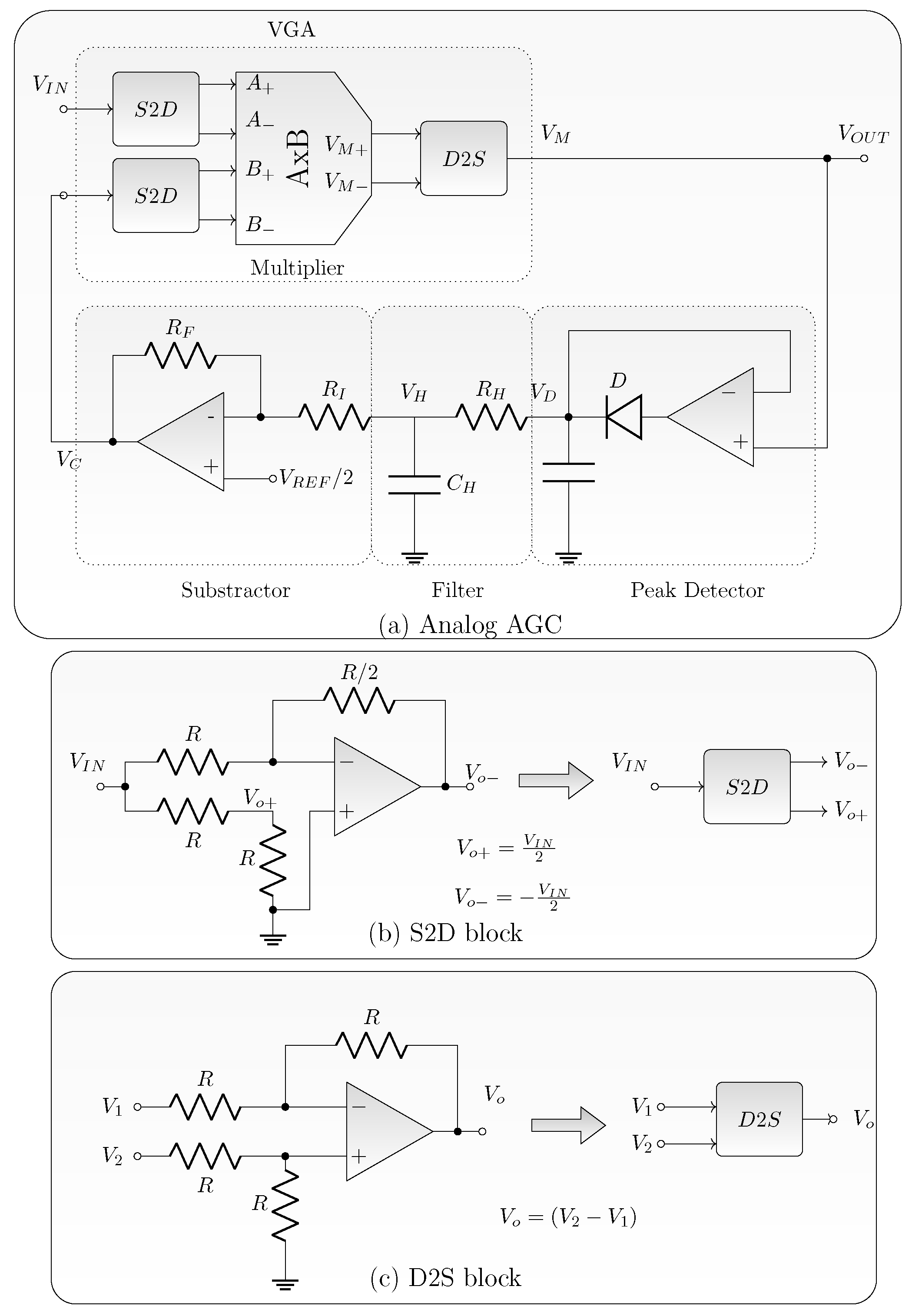
3. Analog AGC
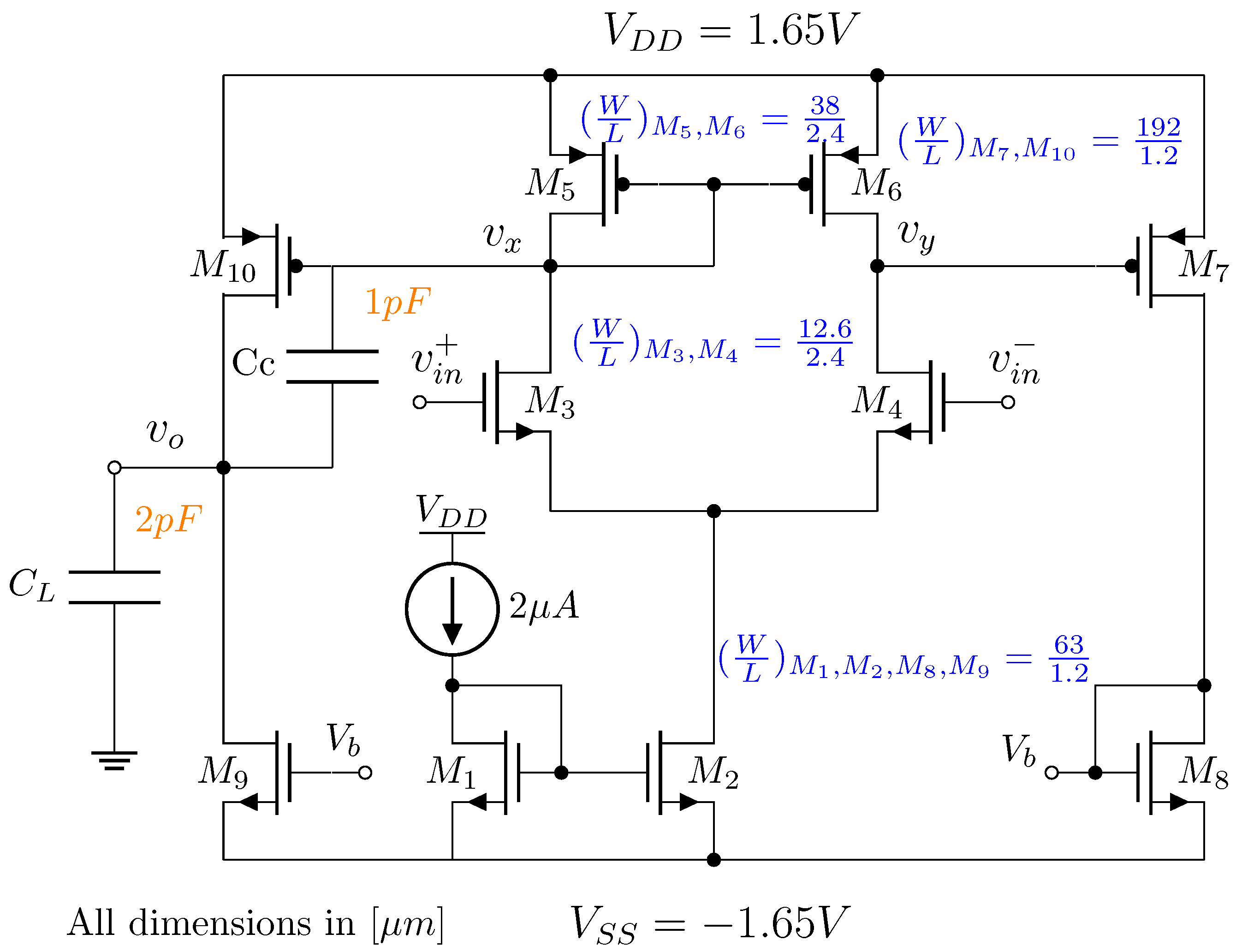
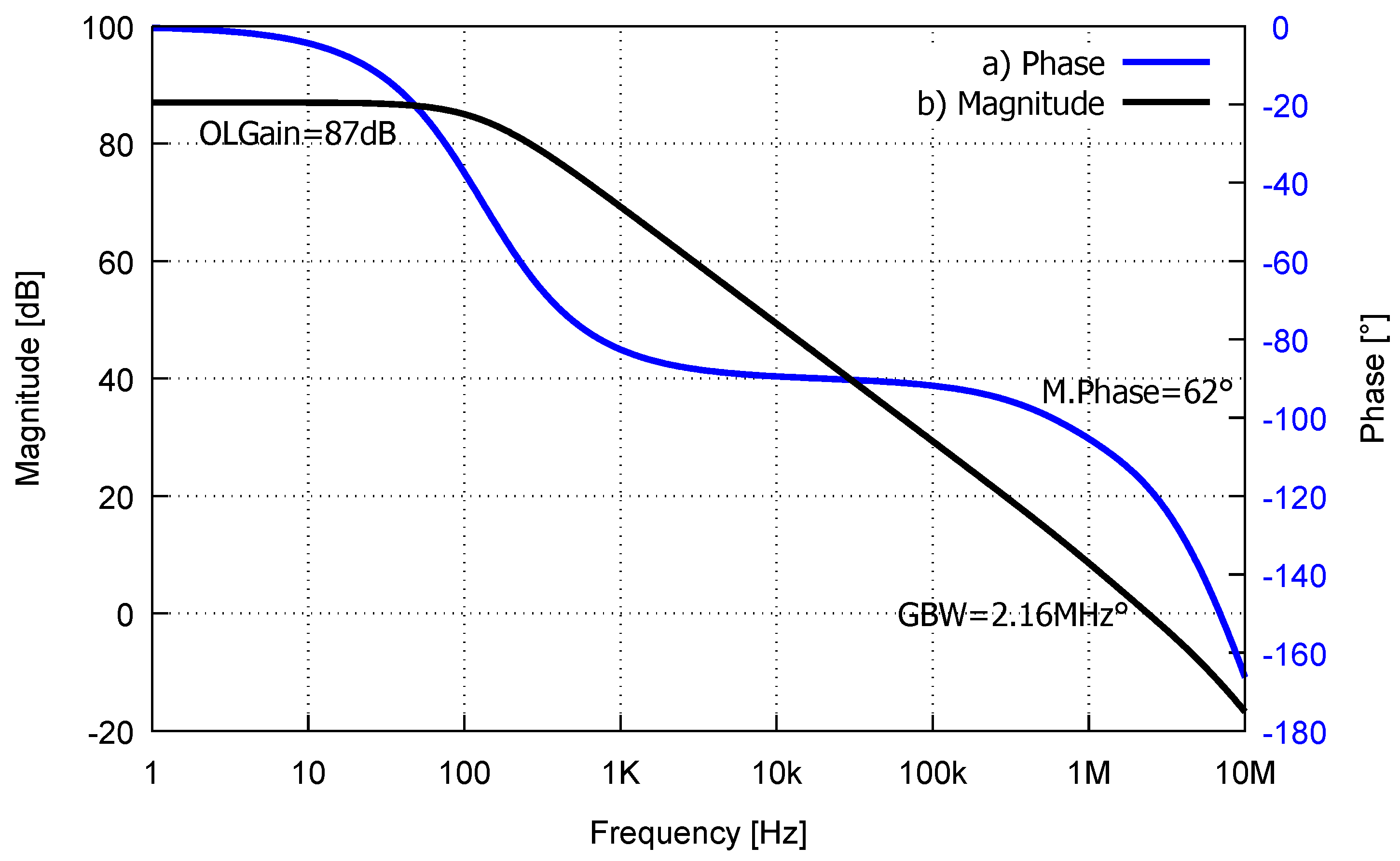
3.1. Operational Amplifier
- We determine the necessary transconductance of differential pair () for a GBW = 2 MHz and a lod capacitance() of 2 pF as shown in Equation (1).
- We find the aspect ratio of transistor N for a = 0.08 V, = 57 A/V = and = 2 A, as shown in Equation (2).
- Using Equation (3), we propose an = 2.4 m and obtain a .
- Due to the difference between = 57 A/V and = 18 A/V, is calculated using Equation (4).
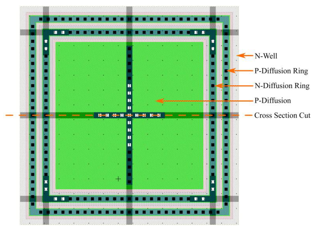
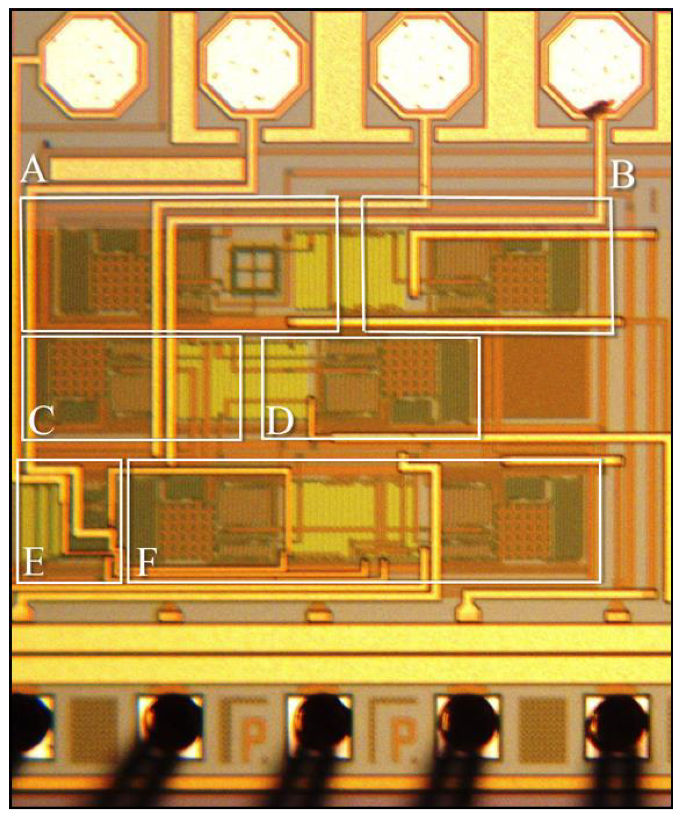
- The dimensions of = 192 m/1.2 m and = 63 m/1.2 m are proposed to handle 8, as shown in Figure 5.
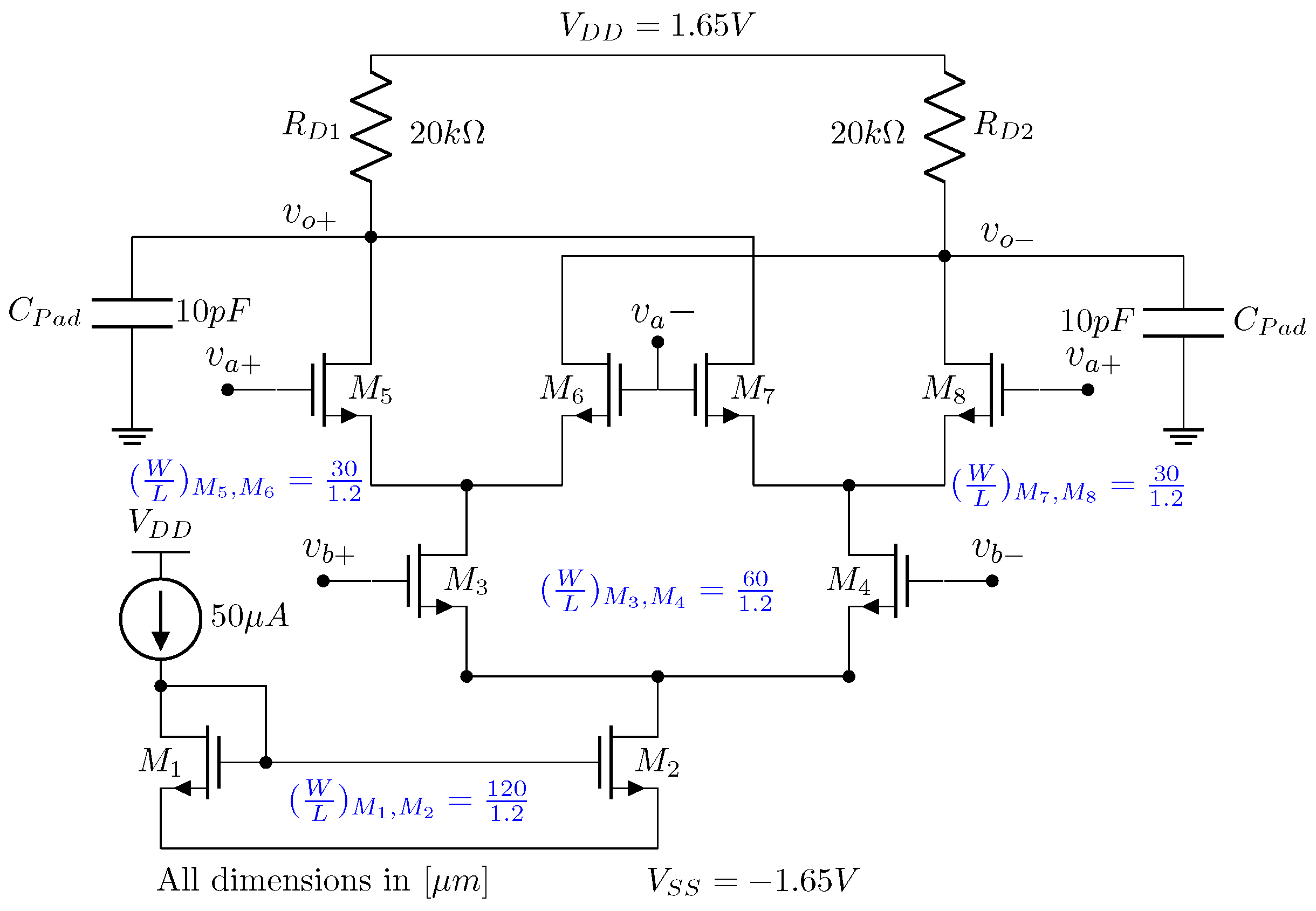
3.2. Four-Quadrant Analog Multiplier
3.3. Peak Detector
3.4. Subtractor
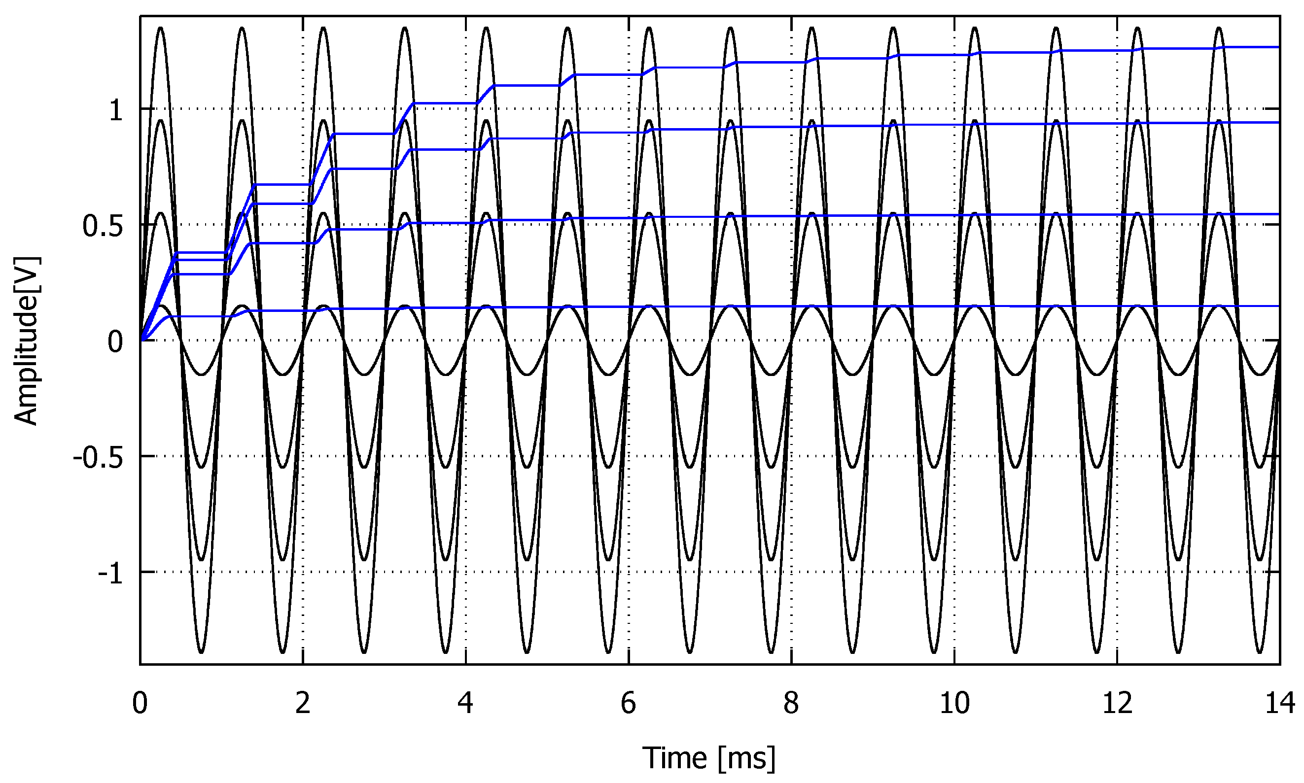
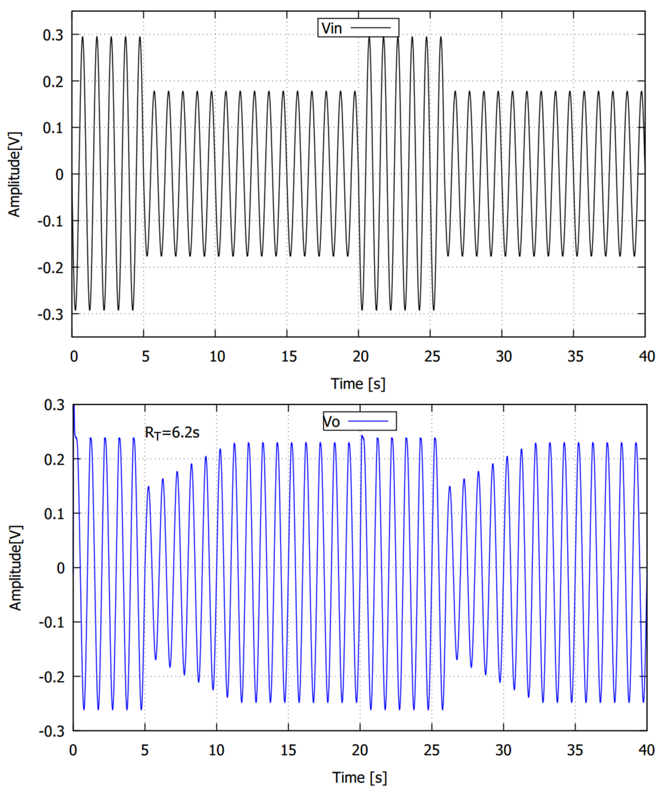
4. Analog AGC Simulation Results
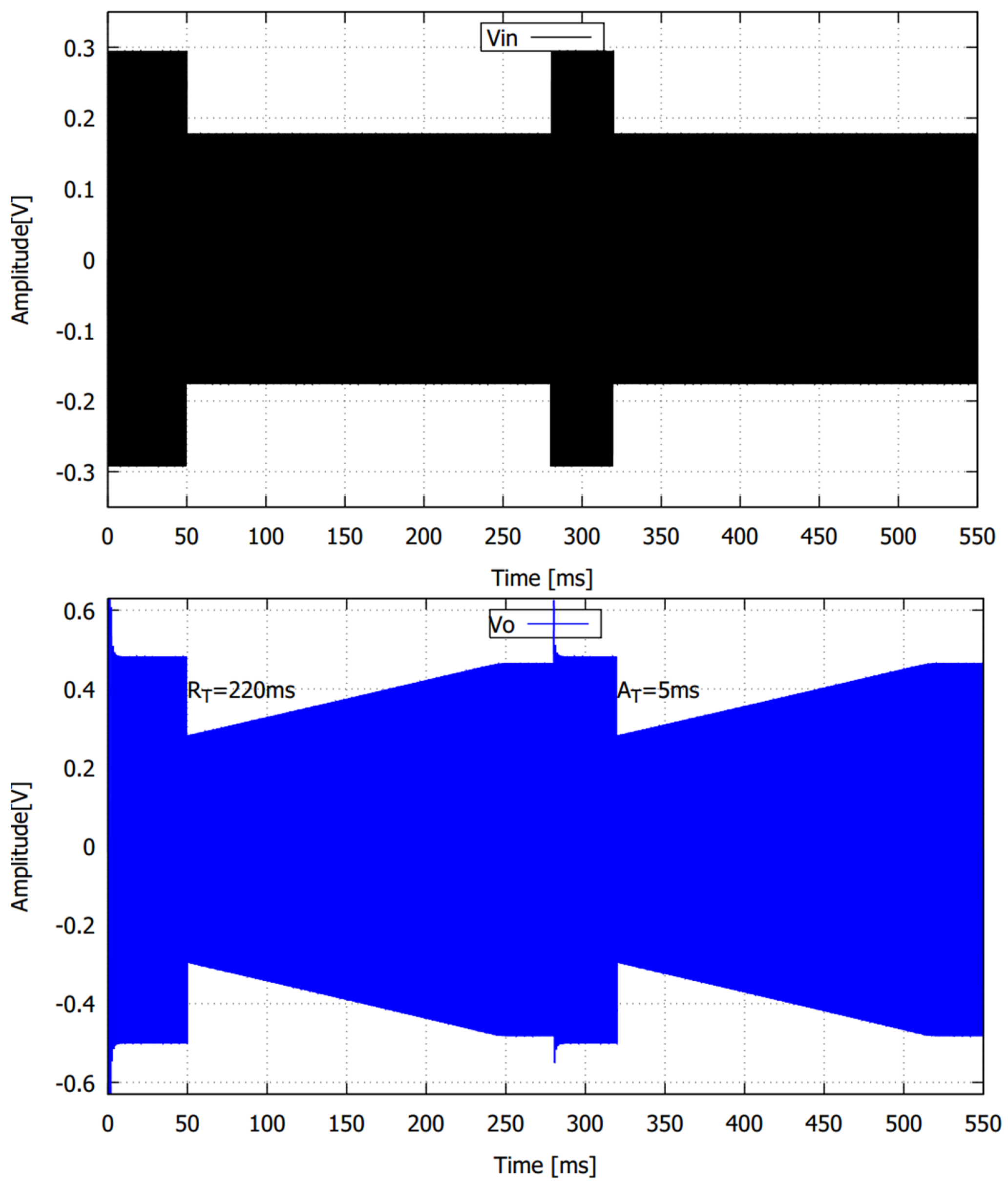
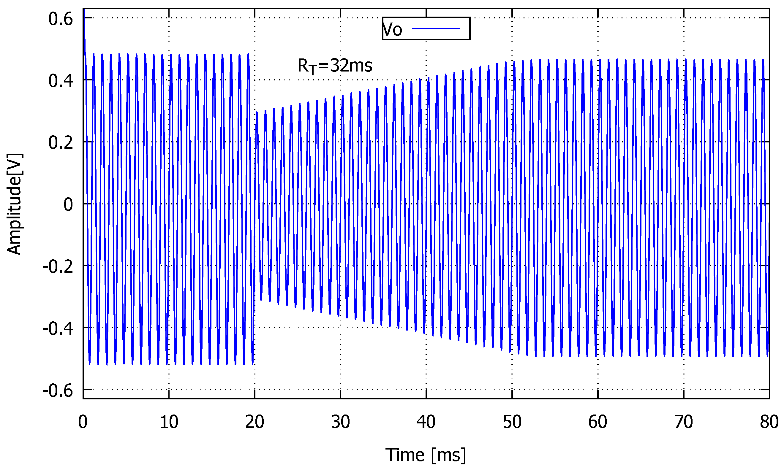
5. Experimental Results and Discussions
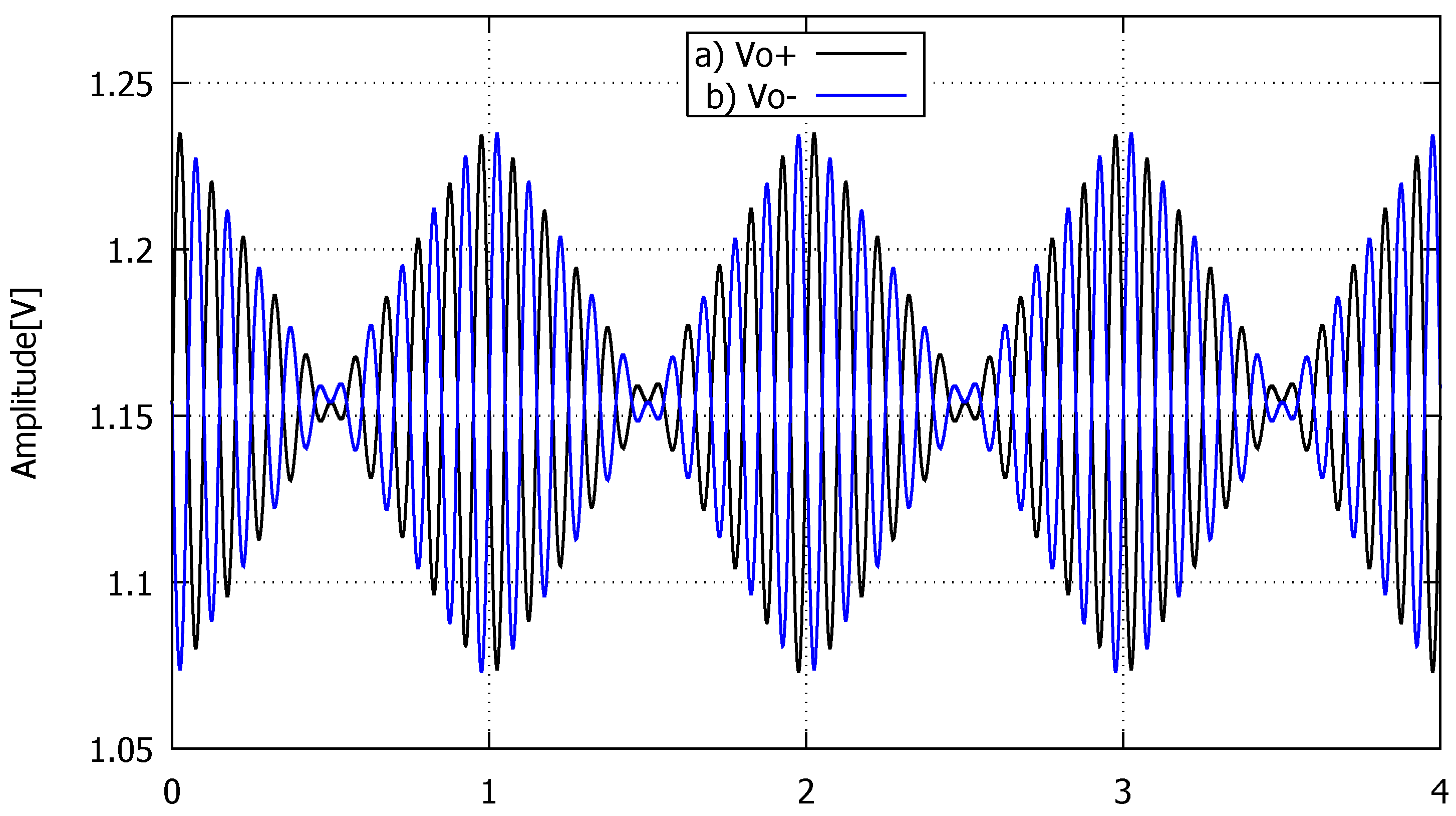
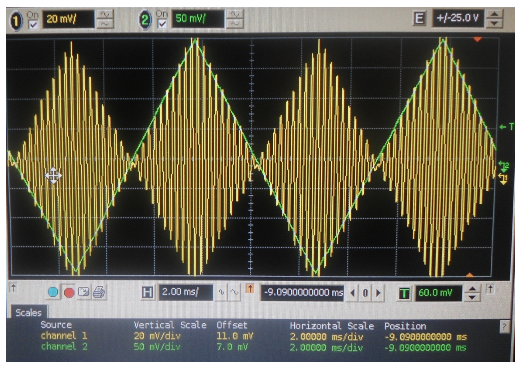
5.1. Analog Four-Quadrant Multiplier
5.2. Peak Detector
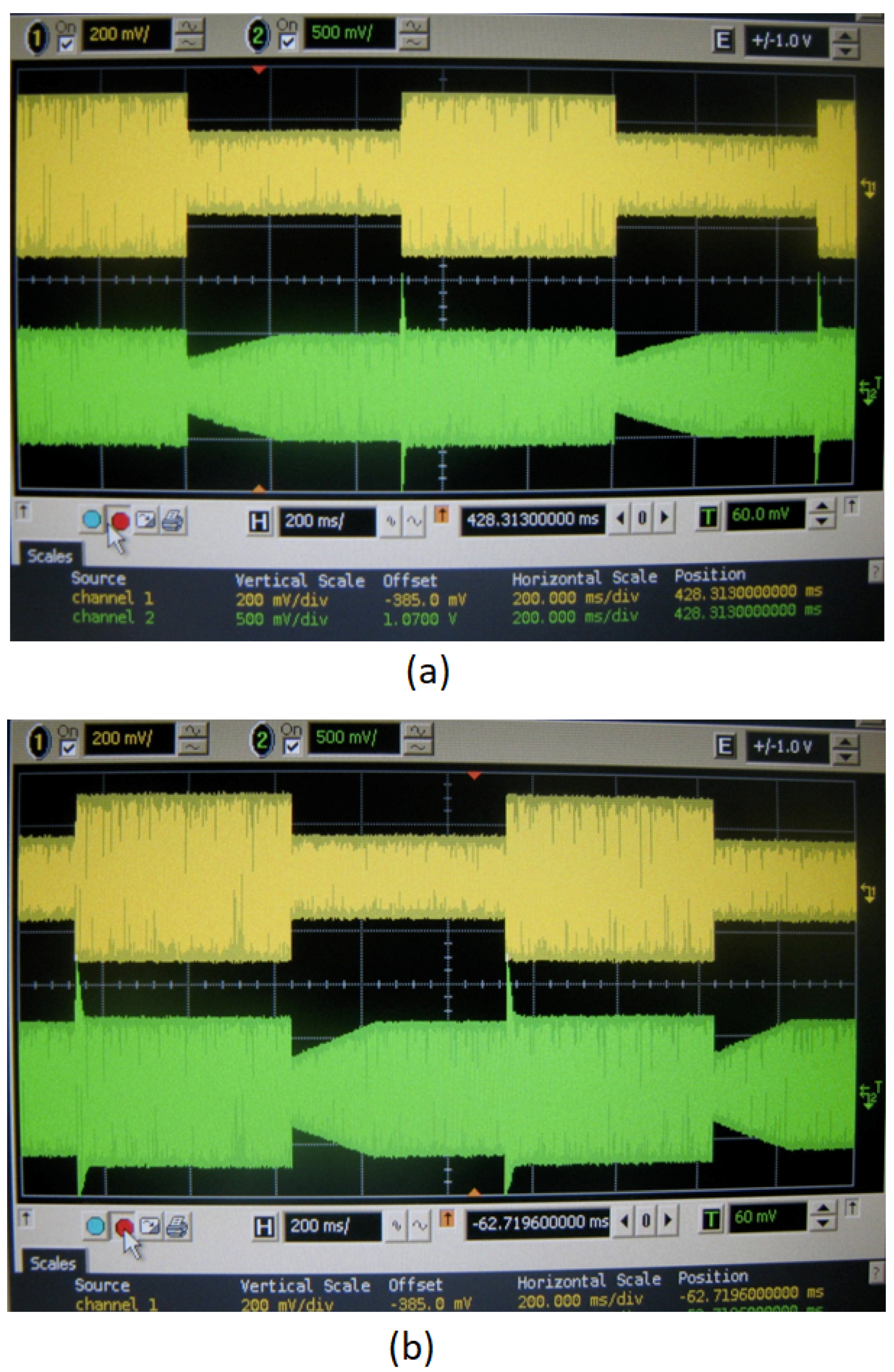
5.3. Complete Analog AGC
6. Conclusions
Author Contributions
Funding
Acknowledgments
Conflicts of Interest
References
- Organización Mundial de la Salud. Las 10 Principales Causas de Defunción. Available online: https://www.who.int/es/news-room/fact-sheets/detail/the-top-10-causes-of-death (accessed on 6 March 2020).
- Koydemir, H.C.; Ozcan, A. Wearable and implantable sensors for biomedical applications. Annu. Rev. Anal. Chem. 2018, 11, 127–146. [Google Scholar] [CrossRef] [PubMed]
- Steyaert, M.; van Roermund, A.H.; Casier, H. (Eds.) Analog Circuit Design: High-Speed Clock and Data Recovery, High-Performance Amplifiers, Power Management; Springer: Berlin/Heidelberg, Germany, 2008. [Google Scholar]
- Huang, Y.C.; Yang, T.S.; Hsu, S.H.; Chen, X.Z.; Chiou, J.C. A novel pseudo resistor structure for biomedical front-end amplifiers. In Proceedings of the 2015 37th Annual International Conference of the IEEE Engineering in Medicine and Biology Society (EMBC), Milano, Italy, 25–29 August 2015; pp. 2713–2716. [Google Scholar]
- Zhang, J.; Chan, S.C.; Li, H.; Zhang, N.; Wang, L. An Area-Efficient and Highly Linear Reconfigurable Continuous-Time Filter for Biomedical Sensor Applications. Sensors 2020, 20, 2065. [Google Scholar] [CrossRef] [PubMed] [Green Version]
- Pourashraf, S.; Ramirez-Angulo, J.; Lopez-Martin, A.J.; Carvajal, R.G.; Díaz-Sánchez, A. ±0.18-V supply voltage gate-driven PGA with 0.7-Hz to 2-kHz constant bandwidth and 0.15-μW power dissipation. Int. J. Circuit Theory Appl. 2018, 46, 272–279. [Google Scholar] [CrossRef]
- Kong, L.; Chen, Y.; Boon, C.C.; Mak, P.I.; Martins, R.P. A Wideband Inductorless dB-Linear Automatic Gain Control Amplifier Using a Single-Branch Negative Exponential Generator for Wireline Applications. IEEE Trans. Circuits Syst. I Regul. Pap. 2018, 65, 3196–3206. [Google Scholar] [CrossRef]
- Bai, C.; Wu, J.; Zhang, M. A CMOS low power fast-settling AGC amplifier based on integrated RSSI. Analog Integr. Circuits Signal Process. 2016, 87, 379–387. [Google Scholar] [CrossRef]
- Ray, S.; Hella, M.M. A 30–75 dBΩ 2.5 GHz 0.13-μm CMOS Receiver Front-End With Large Input Capacitance Tolerance for Short-Range Optical Communication. IEEE Trans. Circuits Syst. I Regul. Pap. 2016, 63, 1404–1415. [Google Scholar] [CrossRef]
- Hu, Y.; Georgiou, P. An Automatic Gain Control System for ISFET Array Compensation. IEEE Trans. Circuits Syst. I Regul. Pap. 2016, 63, 1511–1520. [Google Scholar] [CrossRef]
- Veugen, L.C.; Chalupper, J.; Snik, A.F.; Opstal, A.; Mens, L.H. Matching Automatic Gain Control Across Devices in Bimodal Cochlear Implant Users. Ear Hear. 2016, 37, 260–270. [Google Scholar] [CrossRef] [PubMed]
- Altoè, A.; Charaziak, K.K.; Shera, C.A. Dynamics of cochlear nonlinearity: Automatic gain control or instantaneous damping? J. Acoust. Soc. Am. 2017, 142, 3510. [Google Scholar] [CrossRef] [PubMed] [Green Version]
- Anderson, S.R.; Easter, K.; Goupell, M.J. Effects of rate and age in processing interaural time and level differences in normal-hearing and bilateral cochlear-implant listeners. J. Acoust. Soc. Am. 2019, 146, 3232–3254. [Google Scholar] [CrossRef] [PubMed]
- Boyle, P.J.; Büchner, A.; Stone, M.A.; Lenarz, T.; Moore, B.C. Comparison of dual-time constant and fast-acting automatic gain control (AGC) systems in cochlear implants. Int. J. Audiol. 2009, 48, 211–221. [Google Scholar] [CrossRef] [PubMed]
- Hsu, Y.P.; Lin, Y.T.; Chen, C.H.; Lu, S.S. A Feed-Forward Automatic-Gain Control Amplifier for Biomedical Applications. In Proceedings of the 2007 Asia-Pacific Microwave Conference, Bangkok, Thailand, 11–14 December 2007. [Google Scholar]
- Kim, S.; Cho, N.; Song, S.J.; Yoo, H.J. A 0.9 V 96 μW fully operationa digital hearing aid chip. IEEE J. Solid-State Circuits 2007, 42, 2432–2440. [Google Scholar] [CrossRef]
- Baker, M.W.; Sarpeshkar, R. Low-power single-loop and dual-loop agcs for bionic ears. IEEE J. Solid-State Circuits 2006, 41, 1983–1996. [Google Scholar] [CrossRef]
- Sugiyama, A.; Miyahara, R. Automatic gain control with integrated signal enhancement for specified target and background-noise levels. In Proceedings of the 2017 IEEE International Conference on Acoustics, Speech and Signal Processing (ICASSP), New Orleans, LA, USA, 5–9 March 2017; pp. 5640–5644. [Google Scholar]
- Zeng, Q.; Delisle, G.Y. Path loss model for ultra wideband signal propagation. In Proceedings of the 2006 12th International Symposium on Antenna Technology and Applied Electromagnetics and Canadian Radio Sciences Conference, Montreal, QC, Canada, 17–19 July 2006. [Google Scholar]
- Tian, X.; Bai, C.; Wu, J.; Zhang, M.; Ji, X. A low power dB-linear RSSI based on logarithmic amplifier. IEICE Electron. Express 2014, 11. [Google Scholar] [CrossRef] [Green Version]
- Zeeshan, M.; Mehtab, Z.; Khan, M.W. A fast convergence feedforward automatic gain control algorithm based on RF characterization of Software Defined Radio. In Proceedings of the 2016 International Conference on Advances in Electrical, Electronic and Systems Engineering (ICAEES), Putrajaya, Malaysia, 14–16 November 2016; pp. 100–104. [Google Scholar]
- Cheng, X.; Xie, G.; Zhang, Z.; Yang, Y. Fast-Settling Feedforward Automatic Gain Control Based on a New Gain Control Approach. IEEE Trans. Circuits Syst. II Express Briefs 2014, 61, 651–655. [Google Scholar] [CrossRef]
- Li, F.; Yang, H.; Wang, Y.; Wu, Q. Current mode feed-forward gain control for 0.8 V CMOS hearing aid. In Proceedings of the 2011 IEEE International Symposium of Circuits and Systems (ISCAS), Rio de Janeiro, Brazil, 15–19 May 2011; pp. 793–796. [Google Scholar]
- Alegre Pérez, J.P.; Pueyo, S.C.; Pueyo, B.C. Automatic Gain Control: Techniques and Architectures for RF Receivers; Springer: Berlin/Heidelberg, Germany, 2011. [Google Scholar]
- Lemus-Lopez, J.; Diaz-Sanchez, A.; NIZ-MONTERO, C.M.; Ramirez-Angulo, J.; Rocha-Pérez, J.M.; Sanchez-Gaspariano, L.A. High Gain Amplifier with Enhanced Cascoded Compensation. Radioengineering 2014, 23, 505. [Google Scholar]
- Gilbert, B. A precise four-quadrant multiplier with subnanosecond response. IEEE J. Solid-State Circuits 1968, 3, 365–373. [Google Scholar] [CrossRef]


| Biomedica Signal | Frequency (Hz) | Amplitude |
|---|---|---|
| ECG (Electrocardiogram) | 0.01–300 | 0.05–3 (mV) |
| EEG (electroencephalogram) | 0.1–100 | 0.001–1 (mV) |
| EOG (Electro-oculogram ) | 0.1–10 | 0.0001–0.03 (mV) |
| EMG (Electromyogram) | 50–3000 | 0.001–100 (mV) |
| PPG (Photoplethysmography) | <10 | >95% (Levels of SpO) |
| Body temperature | 0–0.1 | 32–40 (C) |
| Blood pressure | 0–50 | 10–400 (mm Hg) |
| Respiratory rate | 0.1–10 | 2–50 (Breaths/min) |
| Simulations | Simulations | Experimental | Experimental | ||
|---|---|---|---|---|---|
| [V] | [V] | [V] | [s] | [V] | [s] |
| 300 m, 180 m | 500 m | ≈500 m | 200 m, 1 m | ≈500 m | 210 m, 10 m |
| 300 m, 180 m | 700 m | ≈700 m | 300 m, 1 m | ≈700 m | 200 m, 20 m |
| 550 m, 180 m | 750 m | ≈750 m | 430 m, 1 m | ≈700 m | 350 m, 20 m |
| Parameter | Kim [16] | Hu [10] | Baker [17] | This Work |
|---|---|---|---|---|
| Technology | 0.18 m | 0.35 m | 1.5 m | 0.5 m |
| Power consumption | <71 W | 4.8 mW | 32 W | 200 W |
| Type AGC | Digital | Analog | Analog | Analog |
| Vin | 12.5 mV/180 mV | 40 mV to 72 mV | — | 180 mV to 330 mV |
| 62.5 mV–197.5 mV | 97.6 mV | — | 500 mV–700 mV | |
| Test frequency | 1 kHz | 200 kHz | 1 kHz | 1 kHz |
| Release time | — | 1 ms | 70 ms–140 ms | 200 ms |
| Attack time | — | 1 ms | 1 ms–3 ms | 20 ms |
| Supply voltage | 0.9 V | 3.3 V | 2.8 V | 3.3 V |
| Total die area | — | 0.37 mm | 4.41 mm | 0.16 mm |
| AGC control | Voltage-mode | Voltage-mode | Voltage-Mode | Voltage-mode |
| Applications | Hearing aid | Sensor calibration | Bionic Ears | Biomedical signals |
© 2020 by the authors. Licensee MDPI, Basel, Switzerland. This article is an open access article distributed under the terms and conditions of the Creative Commons Attribution (CC BY) license (http://creativecommons.org/licenses/by/4.0/).
Share and Cite
Bolaños-Pérez, R.; Rocha-Pérez, J.M.; Díaz-Sánchez, A.; Ramirez-Angulo, J.; Tlelo-Cuautle, E. CMOS Analog AGC for Biomedical Applications. Electronics 2020, 9, 878. https://doi.org/10.3390/electronics9050878
Bolaños-Pérez R, Rocha-Pérez JM, Díaz-Sánchez A, Ramirez-Angulo J, Tlelo-Cuautle E. CMOS Analog AGC for Biomedical Applications. Electronics. 2020; 9(5):878. https://doi.org/10.3390/electronics9050878
Chicago/Turabian StyleBolaños-Pérez, Ricardo, José Miguel Rocha-Pérez, Alejandro Díaz-Sánchez, Jaime Ramirez-Angulo, and Esteban Tlelo-Cuautle. 2020. "CMOS Analog AGC for Biomedical Applications" Electronics 9, no. 5: 878. https://doi.org/10.3390/electronics9050878