1. Introduction
After decades of rapid development, large-scale integrated circuits have become the backbone of information technologies. In the past, the integrated circuits (IC) fabricating process continues to develop along with Moore’s Law, 7 nm-process has now entered the production stage, 5 nm and 3 nm process is also steadily advancing. Every breakthrough in the process node leads to a better performance and lower power consumption [
1]. However, as the complexity of the IC manufacturing process increases dramatically, the cost of tape-out rises greatly. For example, the design cost is 300M for building a new graphics processing unit (GPU), central processing unit (CPU) or system on chip (SoC) [
2], which brings great challenges for the design of the chips in multiple fields.
The slowdown and stagnation of Moore’s law [
3] and Dennard scaling [
4] exacerbate this problem. To be specific, Moore’s Law shows signs of slowdown since 2000. The gap between predictions of Moore’s Law and the actual performance of chips grew by 15 times by 2008. Dennard scaling began to slow down significantly in 2007 and nearly lapsed in 2012. The improvement of performance and power consumption in the chip becomes less cost-effective with the upgrade of the IC manufacturing process. Industry and academia generally believe that the Post Moore’s Era [
5] will come soon, which means longer-term research will focus on the More Moore technologies and efforts should be made in every aspect of semiconductor industry along with scaling process such as design, device architectures, package process, even new devices beyond-CMOS to sustain power, performance, area and cost (PPAC) scaling [
6].
As efforts towards integration technology under the More Moore framework, chiplet-based design technology has gained widespread attention for solving the above problems from three aspects. Firstly, chiplets try to integrate multiple modular chips (the main form of modular chips is die.) into a single package for developing dedicated heterogeneous chips via internal interconnection technology. This solution solves the problems of scale, development costs and period efficiently. Secondly, with 2.5D, 3D and other advanced packaging technologies, chiplets achieves high-performance multi-chip on-chip interconnection, which improves the integration of the chip system and the optimizations of performance and power consumption. Finally, modular integration not only accelerates the development speed effectively, but also reduces the development cost and the threshold. Therefore, the research and development of chips focus on algorithms and core technologies, improving the overall innovation level and capabilities greatly.
Compared to the traditional monolithic integration method, chiplets have advantages and potentials in many aspects. However, there are many challenges for promoting the maturity and widespread application of chiplets. Firstly, the unified interfaces and standards are essential for heterogeneous integrated systems. The design of interconnect interfaces and standards for diverse heterogeneous chips face difficulties in balancing performance and flexibility in terms of technology and competitions for market domination. Secondly, the core packaging technologies of chiplets face challenges in performance, power consumption, cost, and so forth. Thirdly, a critical issue to be solved for chiplets is whether the electronics design automation (EDA) toolchains and ecological system that supports the design and implementation of chips is complete and sustainable.
Currently, chiplets have been successfully applied in industry, especially companies with high-end technologies and research capabilities. HBM memory [
7] is a typical representation of early successful application. Since then, in the FPGA-related fields, Intel company introduced the Agilex field programmable gate array (FPGA) productions based on chiplet technology. These productions use 3D packaging technology to achieve heterogeneous chip integration. In the field of high-performance CPU chips, AMD introduced Zen 2 architecture [
8] that separates IO components and processor cores into multiple small chips (using 7 nm, 14 nm and other process) for further on-demand integration [
9]. In the field of networking, Intel (formerly Barefoot)’s Tofino2 chip, with 12.8 T switching capability, is implemented via chiplets. It integrates the switching logic chip with a high-speed SerDes chip. Recently, in academia, University of California, Georgia Institute of Technology, and European research institutions [
10,
11] begin to research the chiplet-related problems, including the interconnect interfaces, packaging, and applications.
These above researches mainly focus on independent products or local technologies. Differently, the CHIPS plan (Generic Heterogeneous Integration and IP Reuse Strategy [
12]) launched by DARPA (US Department of Defense Advanced Research Projects Agency) in 2017 attempts to push chiplets to the level of strategic unification and ecological construction. In DARPA’s planning, chiplets involves dies with different function from different companies, different process node, different semiconductor materials, different signal types (i.e., wave, electron, photon, even microelectromechanical system). Thus, chiplet technology is designed to support a huge technical roadmap in new ecology and application system.
Despite the widespread attention of the chiplet technology, the review article about chiplets is scarce and urgently needed. In this paper, we analyze the existing research and applications about chiplets in detail and propose future development trends. We wish that our efforts could provide references for researchers engaged in the research and design of the next-generation chips.
2. Overview of Chiplets
Traditionally, there are two ways for IC designers to develop their next generation IC productions. The mainstream method is directly transporting old design into smaller process node to obtain higher device frequency for better PPA. The second way is to incorporate more functional blocks under same process node to reduce the cost in mask and EDA tools [
13].
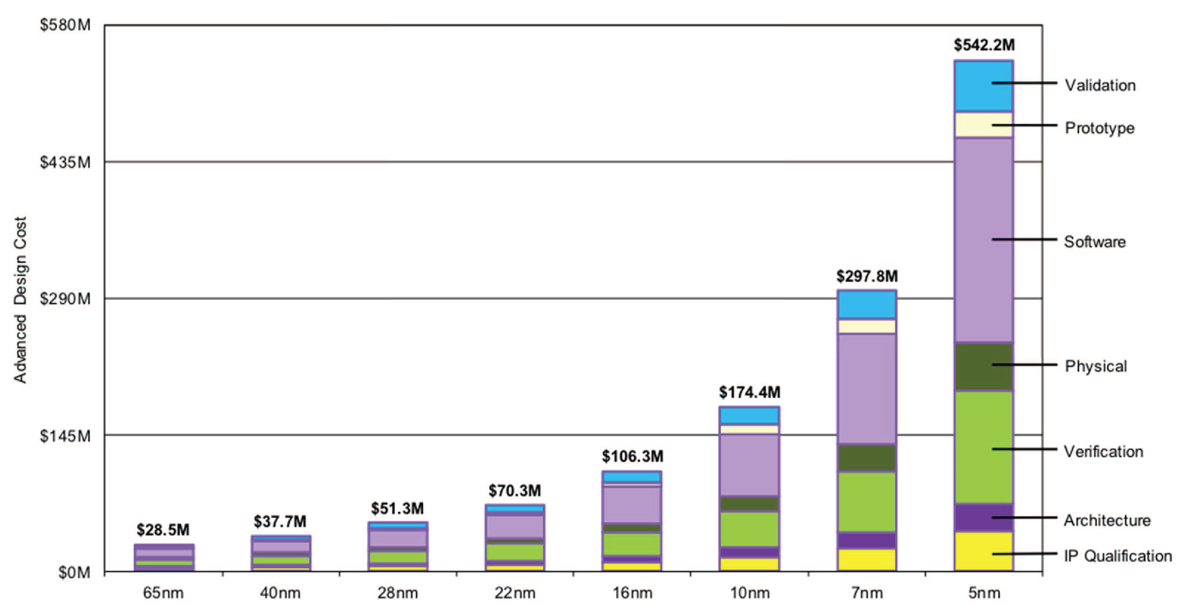
However, with the evolution of chip manufacturing process, the overall chip design cost has increased significantly due to the more complicated process and more difficult design and implementation. According to the survey from the International Business Strategy Corporation (IBS), the increase of design cost for each generation technology has exceeded 50% after 22 nm process, including EDA, design verification, IP core, tape-out, and so forth. For instance, the total design cost of 7 nm process is about 300 million dollars, and that of 3 nm process is expected to increase 5 times up to 1.5 billion dollars [
2], as depicted in
Figure 1. Thus, the difficulties for implementing a high-performance chip upgrade based on process improvement are increasing and the price-performance ratio is increasing. Furthermore, due to the technical limitations in yield (such as the mask size of lithography machine), the existing monolithic integration becomes unsustainable with new process for upgrading and expanding the functions and performance.
In such a scenario, chiplets provide a feasible way for future chip design. Multi-Chip Modules (MCM) technology [
14], which appeared in the 1980s, has already embodied the concept of chiplets. MCM technology connects multiple chips on a substrate or other medium for meeting the performance and functional requirements of complex system chips. MCM could reduce the overhead of board-level interconnection and the complexity of board-level system design, which saves the cost of building a system greatly. Recently, Intel, AMD, and other companies have developed a series of high-performance chip products based on MCM technology. However, MCM mainly focuses on the underlying packaging technology. And it does not consider the high-level problems on heterogeneous integration of chip, including multi-level interconnection standards, interfaces, tools, and ecology.
In 2017, DARPA planned the “General Heterogeneous Integration and IP Reuse Strategy [
12]” (CHIPS) in the “Electronic Revival Plan”. This project attempts to utilize the industrial and academic forces to solve the above problems. The participants consist of the system integration vendors (Lockheed Martin, Northrop Grumman, Boeing, Intel, Micron, etc.), EDA vendors (Cadence, Synopsys, etc.) and research institutions (University of Michigan, Georgia Institute of Technology and North Carolina State University, etc.). This project emphasizes on developing a new technology framework that incorporates chip dies with different functions, then matches and combines them onto the interposer. It not only integrates dies into on-chip systems at a lower cost, but also enhances the overall flexibility and reduces the design time of next-generation products.
The Open Compute Project (OCP) promoted by Facebook and other companies also actively launched the Open Domain-Specific Architecture (ODSA) [
15] research at the end of 2018. It tries to develop a complete architecture interface stack and to create a chiplet open market. By defining open standardized interfaces, the die integrated in Chiplet chips could interoperate to support the flexible combination from different vendors for building more flexible chip systems.
To achieve these above goals, the research and development of software toolchains and the typical applications will be the important problems to be addressed for further development of chiplets. To be specific, the software toolchains includes the full-stack feasible interconnection interface specifications and standards at the physical layer, link layer, and network layer, advanced chip packaging technologies, yield-oriented EDA, and so forth.
3. Advantages of Chiplets
Compared to the traditional printed circuit board (PCB) board integration and monolithic ASIC integration, the advantages of chiplets mainly reflected in technology, development cost, and business.
Technology. Chiplets improve the optimization potentials on performance and power consumption by recombining multiple small chips. Thus, it supports the domain-specific customization and mitigating the effect from the slowdown of Moore’s law for developing diverse chips. For instance, high-speed SerDes has higher requirements on power consumption for the network chips with high-density and high-speed interfaces. The network chips based on chiplet technology seperate the high-speed SerDes IO module from the core logic, providing more layout options for the power consumption. This is also an important reason why chiplet technology is applied in Intel’s programmable switching chip Tofino2. Besides, the memory access bandwidth is usually a performance bottleneck for high-performance CPUs and AI chips. Chiplets improve the signal transmission quality and bandwidth and mitigates the "storage wall" issue by combining the processor core and memory chips with 3D stacking technology. This is the key point that AMD and Intel focus and adopt chiplets in the early days.
Development Cost. Chiplets generally integrate multiple small dies into a large monolithic chip with advanced packaging processes. The features of low cost and high yield in small chips that occupy relatively low area could reduce the overall cost effectively [
16]. In addition to the chip manufacturing cost, the research and development cost gradually takes up a great proportion of the overall chip cost. By combining the known good dies (KGD) directly, the research and development cycle is greatly reduced and the relative investment is saved. The development and manufacturing cost of AMD’s 32 core EPYC CPU is reduced by 40% with chiplets [
17]. Besides, the large-scale high-performance chips, especially commercial chips, usually become mature products and come into market after multiple silicon verifications in traditional monolithic integration. This solution generally results in great pressure on the research and development cost. On the contrary, the chips developed with chiplets usually select the widely used and mature chip dies to integrate, reducing the development risk of chips. Thus, the number of re-spins and packaging is decreased and the cost is saved effectively.
Business. Chiplets could effectively improve the speed of chip development and reduce the related cost and barriers. Thus, scientific research and commercial institutions pay much attention to the core algorithms and technologies, which promotes technological innovation effectively. Besides, the continuous evolution and improvement of the chiplet ecosystem will accelerate the generation of new industries. The business model of chiplets may generate three types of business roles, including chiplet suppliers that supply chiplet modular chips, chiplet integrators that integrate chiplet modular chips to form a complete system, and EDA softwares that provide the tool chains and design automation services. At present, Intel, Micron and other corporations begin to play important roles in the industry chain while startups (like zGlue [
18]) focus on opening up the missing links in the chiplet industry chain.
Table 1 shows the comparisons between chiplet technology and traditional technologies. To be specific, chiplets are very close to a monolithic ASIC chip in terms of performance, power consumption and integration. With respect to the cost and design cycle, there is only a small gap between chiplets and traditional PCB technology. In summary, the chiplet makes a good tradeoff between monolithic ASIC and PCB technology and has great development potential.
4. Challenges of Chiplets
Although chiplets have many advantages as mentioned above, there are still many challenges for further development, including interconnect interfaces and protocols, packaging technology and quality control.
4.1. Interconnect Interfaces and Protocols
The interconnect interfaces and protocols among chiplets is very critical for the development of chiplets. The design of interfaces and protocols must consider the requirements of matching the manufacturing process and packaging technology, system integration, and expansion. Besides, the related performance indexes of chiplets in different fields are also crucial, such as the transmission bandwidth per unit area, power consumption per bit. Generally, the above-mentioned factors are contradictory, which brings greater challenges for the design of interconnected interfaces and protocols.
The interconnect interfaces used by chiplet technology in the physical layer could be divided into the following categories.
4.1.1. Serial Interfaces
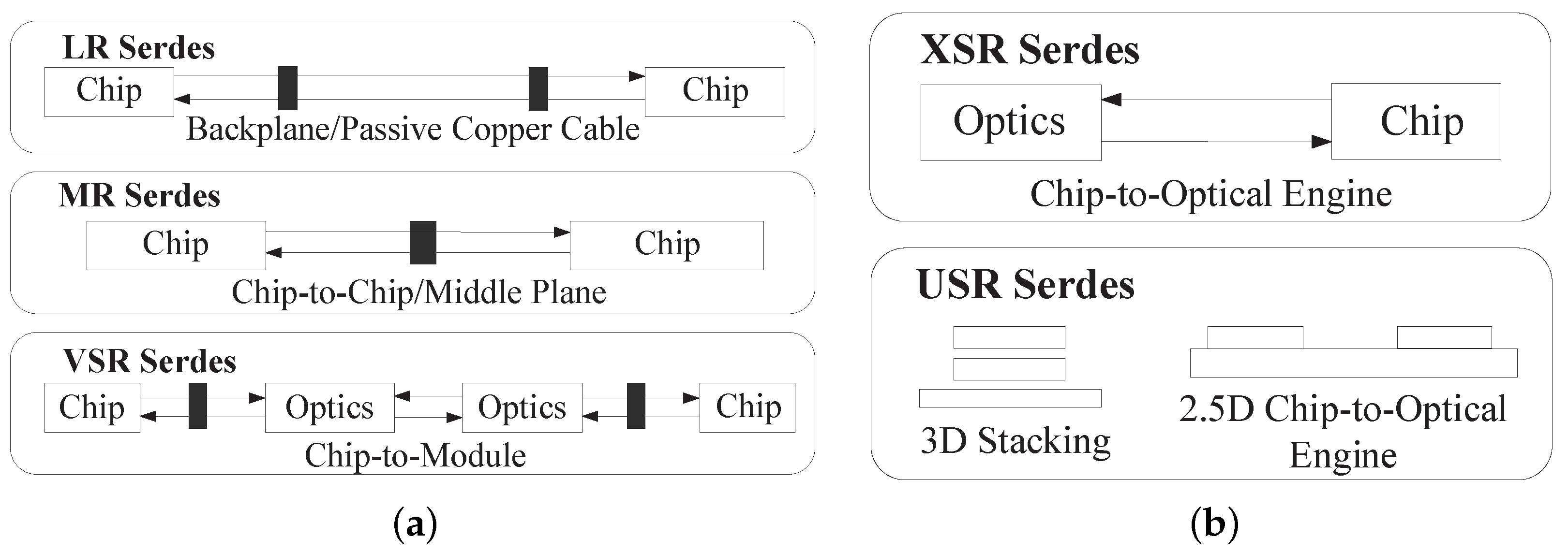
From the perspective of application transmission distance, serial interfaces consist of long reach/medium reach/very short reach SerDes (LR/MR/VSR SerDes), extremely short distance (XSR) SerDes and ultra-short distance (USR) SerDes.
Figure 2 shows that the application scenarios in which these interfaces are applied.
LR/MR/VSR SerDes are generally applied for the inter-chip and chip-to-module connections based on PCB boards. They are widely used to implement communication interfaces such as PCI-E, Ethernet, and RapidIO. The main features of these interfaces are reliable, long transmission distance, low cost, and easy integration. However, since these interfaces have no advantages in power consumption, area and delay, it is difficult to support the construction of high-performance chips that has high requirements on these indexes above.
XSR SerDes provide related SerDes standards for the interconnection of Die-to-Die(D2D) and Die-to-Optical Engine (D2OE). The design of XSR SerDes mainly focuses on the interconnection of D2OE. It is developed based on traditional SerDes structure that integrates the clock data recovery circuit (CDR) and has strict requirements on the cost of insertion loss. To achieve a lower bit error rate, complex forward error correction (FEC) mechanisms are necessary to be integrated. However, it will introduce significant delay and power consumption. Especially when the bandwidth reaches 112 G or higher, the overhead caused by signal reflection would introduce extra delay and power consumption. Moreover, in order to provide good signal integrity, high-performance chip process and packaging substrate materials are demanded to support large-scale integration. XSR is suitable to be deployed between optical devices and bare chips with end-to-end FEC.
Compared to XSR, USR SerDes mainly focuses on implementing high-speed interconnect communication of Die-to-Die at ultra-short distance (10 mm level) via 2.5D/3D packaging technology. Since the communication distance is short, USR provides better performance and power consumption ratio and better scalability with advanced coding, multi-bit transmission, and other technologies. For example, Kandou’s Glasswing 112 G USR SerDes using CNRZ-5 encoding could achieve 0.72 pJ/bit power consumption, and 224 G SerDes could achieve 0.8 pJ/bit [
19]. Since the implementation of USR interface generally involves patented technologies (such as encoding methods), its interoperability compatibility faces greater challenges. Besides, the requirements of USR on the transmission distance impede the integration of large-scale chiplets.
According to the 56 G SerDes interface specification defined by Reference [
20], a comprehensive comparison of multiple interfaces is presented in terms of transmission, application, and other aspects, as shown in
Table 2.
4.1.2. Parallel Interfaces
At present, the generic parallel interfaces for the interconnections of chiplet dies are Intel’s AIB/MDIO [
21], TSMC’s LIPINCON, OCP’s BoW [
22], and so forth. HBM interface also belongs to this type of interface and is dedicated to the interconnections among high-bandwidth storages.
Intel’s AIB (Advanced Interface Bus), a parallel interconnection standard in the physical layer, is similar to the DDR DRAM Interface. In DARPA’s CHIPS project, Intel provides free AIB interface licenses to related vendors for supporting the broad chiplet ecosystem. As an upgraded version of AIB, MIDO provides higher transmission efficiency, and the response speed and bandwidth density are over two times than that of AIB. AIB and MDIO technologies are mainly suitable for 2.5D and 3D packaging technologies with short communication distance and low loss, such as EMIB [
23], Foveros [
24].
LIPINCON [
25] is a high-performance interconnect interface proposed by TSMC for chiplets. By using advanced silicon-based interconnect packaging technologies (such as InFO and CoWoS) and timing compensation technology, LIPINCON could reduce power consumption and area overhead without PLL/DLL. The LIPINCON interface contains two types of PHY: PHYC and PHYM. PHYC is used for SoC die while PHYM is for memory and transceiver dies.
The BoW interface proposed by the OCP ODSA group focuses on solving the organic substrate-based parallel interconnection problems. There are three types of BoW, namely BoW-Base, BoW-Fast, and BoW-Turbo. BoW-Base is designed for the transmission distances below 10 mm and uses unterminated unidirectional interfaces. The data transmission rate of each line could reach up to 4 Gbps. With respect to BoW-Fast, it uses terminated interfaces and the cable length is up to 50 mm. The transmission rate per line is 16 Gbps. Compared to BoW-Fast, Bow-Turbo uses two wires to support bidirectional 16 Gbps transmission bandwidth. Moreover, BoW supports backward compatibility and has fewer restrictions on chip process and packaging technology. It does not rely on advanced silicon-based interconnection packaging technology and has a wide range of applications. These parallel interfaces of chiplets in the physical layer are compared in terms of encapsulation, transmission rate and bandwidth density, as described in
Table 3.
The above mentioned advanced electrical signal interface in the physical layer has achieved a low power consumption on per-bit data transmission. Whereas, as the bandwidth requirements of high-performance network and computing grow dramatically, the increase in power consumption caused by data transmission is still a critical challenge for chip development. Mark Wade et al. proposed to use the optoelectronics hybrid technology to solve IO bottlenecks, which provides new ideas for the development of interconnect technologies and standards with high-performance and low power consumption.
All the above interface standards are designed based on the specific interconnection requirements and the optimal chiplet interconnection solution is related to specific applications. Although parallel interfaces provide low power consumption, low latency, and high bandwidth, it requires more routing resources. On the contrary, serial interfaces require fewer routing resources, but it brings more power consumption and delay. Therefore, chiplet designers must select one or more interfaces in the physical layer for achieving the goal of system optimization according to the actual application requirements, constraints and die features.
4.1.3. Other Interfaces
In principle, traditional interface standards (such as Ethernet MAC, PCIe, etc.) could be used for the transmission of chiplets at the link layer by adapting to the underlying physical layer (PHY). Tilelink interface protocol receives widespread attention for its openness and open-source mode. It attempts to decouple the implementation of the on-chip network and cache controller from the cache consistency protocol. Any cache consistency protocol that follows the Tilelink transaction structure could be used in conjunction with any physical layer network and cache controller. The CCIX [
26] interface standard is designed specifically for the inter-chip accelerator structure. It supports the cache consistency by extending functions in the transaction layer and protocol layer over the standard PCIe data link layer. CCIX also supports flexible topologies and is mainly used for communication between the main CPU and accelerators.
In order to improve the scalability of synchronous communication mechanisms (such as Tilelink, CCIX), an active participant of the OSDA project, namely Netronome, designed the ISF interface protocol. ISF is a lightweight message protocol that supports asynchronous storage access and consists of transport layer, network layer, and link layer. ISF was originally used for the interconnections of on-chip components on the NFP network stream processor of Netronome and It would support the interconnection of Die-to-Die of chiplets.
Different from the industry that closely researches chiplet-related interconnect standards and specifications, the academia mainly focuses on the design and optimizations of the NOC architecture and algorithms between dies in the network layer. Besides, much attention is paid to the implementation of high-performance on-chip network communication based on the active intermediary layer [
16,
27,
28].
4.2. Packaging Technology
The physical implementation of die interconnection in chiplets depends on the completion of the chip packaging process. The performance, cost, and maturity of multi-chip packaging technology affect the application of chiplets greatly. As shown in
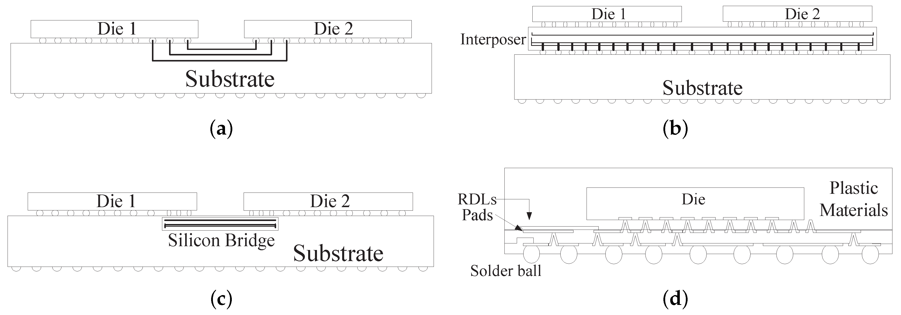
Figure 3, the packaging technologies that support interconnections of chiplets could be divided into three types according to the difference of connection media and processes. They are substrate-based packaging technologies, silicon interposers-based packaging technologies and RDL-based (Redistribution Layer) fan-out packaging technology.
At present, organic substrates are widely used due to the cost and other factors. Similar to the traditional PCB, the organic substrate materials complete the wiring connections with the etching process, which does not depend on the silicon process used in the semiconductor equipment. Multiple dies could be connected with high density on the substrate through wire bonding or flip-chip technology. Since the substrate-based packaging method does not rely on the chip foundry process, the related materials and production cost is low. With this method, the packaging size could be up to 110 mm × 110 mm (Land Grid Array Packaging, LGA) and it is widely used in large-scale chiplet systems [
29,
30]. However, the density of IO pins is low with wiring bonding and flip-chip and most pins of chip are occupied by the power supply. As a result, the pins used for data transmission are more scarce and the external bandwidth of the full chip is limited. Moreover, the crosstalk effect impedes the improvement of the transmission capability of a single pin. Furthermore, these above problems would also limit the transmission bandwidth of Die-to-Die connections and affect the development of chiplets with higher performance.
The 2.5D/3D packaging technologies are mainly in the form of silicon interposer-based packaging technology. The interconnection and communication between dies are implemented by placing an extra silicon layer between the substrate and die. The connection between die and substrate is achieved with through-silicon vias (TSVs) and Micro-Bumps. Since micro-bumps and TSVs have smaller bump pitch and trace distance, silicon interposer-based packaging technology provides a higher IO density and lower transmission delay and power consumption. However, compared to the organic substrate, the implementation of silicon interposer provided by the chip foundry brings higher cost in materials and process. To solve this problem, Silicon Bridge technology attempts to combine the substrate-based and silicon interposer-based technology. It integrates small thin layers on the substrate for inter-die interconnection (less than 75 um [
22]), which makes a good balance between performance and cost. Generally, there are two types of silicon interposers: one is a passive interposer that only contains the connection circuits, and the other is an active interposer that not only contains the connection circuits but also integrates the logic circuits. Although the implementation cost of active interposers is more expensive, it could provide more flexible and extensible solutions than passive interposers [
31,
32]. Therefore, academia focuses more on active interposers.
The substrate-less fan-out packaging technology based on the redistribution layer (RDL) deposits metal and dielectric layers on the surface of the wafer. It forms a redistribution layer to carry the corresponding metal wiring pattern and rearranges the IO ports of chips on the loose area outside the die. In fan-out packaging technology, RDL could enhance the signal quality by shortening the circuit length and improve the chiplet integration by reducing the area of chip. Moreover, fan-out packaging, as a substrate-less packaging method with lower vertical height, provides additional vertical space for more components to be stacked upward. Compared to the silicon interposer-based packaging technology, the cost of fan-out packaging is relatively low. But the wiring resources of fan-out packaging are limited by the RDL wiring level. Since the TSMC’s InFo (Integrated fan-out packaging) technology is applied in the A10 processor of Apple’s iPhone 7 successfully, fan-out technology has received extensive attention from packaging and testing factories and chip foundries. At present, there are more than 10 fan-out packaging technologies in the market launched, providing abundant selections for chiplet integration.
The comparisons of packaging technologies available for chiplet integration are shown in
Table 4. With the continuous development of chiplet technology and the evolution of the related packaging technologies, chiplet technology would gain better support by overcoming the problems about performance, power consumption, cost, and implementability.
4.3. Quality Control Technology
The dies integrated by chiplets are generally silicon-certified products. It could guarantee the validity of its design and physical implementation, but the yield problem would still occur during the filtering and packaging process. As for chiplets, the failure is costly because a problem in a single die would cause the monolithic chip failed. Therefore, perfect and comprehensive testing is particularly important for the quality control of chiplets. Compared with monolithic integration, the difficulty of chip testing is much higher because chiplet packages multiple dies together. Since the pins of chiplets are limited, it only guarantees the connection requirements of some pins and some dies during the test. Thus, it brings new challenges for chiplet comprehensive testing.
The EDA software in chiplets is an important solution to solve this problem. During the chip design and manufacturing process, 30%–40% of the cost is brought from software tools. Chiplets require EDA tools to provide comprehensive support in terms of architecture exploration, chip design, physical and packaging implementation. Therefore, with the intelligent and optimized assistance in each process, human participation is minimized and extra problems are avoided.
Currently, many research institutions and companies in academia and industry have started lots of productive work. Jinwoo Kim et al. [
11]. from Georgia Institute of Technology introduce the EDA process of 2.5D-based chiplet packaging. It covers and automates the entire design phase of the architecture, circuit, and packaging. Besides, the availability of EDA process is validated by a ROCKET-64 CPU with NOC configured. Moreover, traditional integrated circuit EDA companies, such as Cadence, Synopsys, and Mentor, are developing related tools to support chiplet integration.
5. Applications and Development Trends of Chiplets
Although the standardization of chiplets has just begun, it has demonstrated its unique advantages in many fields, ranging from high-performance CPU, FPGA, network chips to low-end chips for Bluetooth, Internet of Things (IoT) and wearable devices.
In terms of high-performance CPU, AMD’s Zen 2 architecture [
30] builds chiplets by combining multiple processor core dies (7 nm process), IO dies (14 nm process) and memory dies in different process nodes. Thus, the improvement of computing performance from the high-end process could be achieved at a lower cost.
Intel’s Stratix 10 high-performance FPGA was developed with chiplet technology in the early days. It integrates FPGA die and SerDes IO die with AIB interface based on EMIB silicon bridge packaging technology (2.5D). Stratix 10 integrates the dies in 6 process nodes from 3 chip foundries, effectively proving the interoperability of chiplet technology among different foundries. Intel’s Agilex FPGAs use advanced 3D packaging technology for the integration of 10 nm FPGA core and 112 G SerDes. It demonstrates that the feasibility of chiplet technology for building high-tech process and chips with high IO performance.
zGlue company focuses on the development and standardization of low-end and mid-range chiplets. The chiplets that developed and manufactured by zGlue, such as Bluetooth, Internet of Things and WiFi, are developed based on nearly 100 dies from more than 30 companies including ADI, Dialog, Macronix and Vishay. Moreover, zGlue builds a set of basic chiplet EDA toolchains, making it possible to achieve die composition and reuse quickly.
Overall, since chiplets could provide customizability and optimizability in multiple dimensions (such as the yield and cost), it would be widely applied in more fields [
33,
34]. With the rapid rise of open-source ecology and agile development [
35] in the chip field, chiplet approach would become the mainstream technology for chip development in the future. Therefore, it is worthwhile for scientific institutions and industry to research the relevant technical challenges and issues deeply.
6. Conclusions
By summary, this paper introduces the concept of chiplet technology and its developments. As a possible solution to break the slowdown of Moore’s law, chiplet heterogeneous integration technology has received widespread attention in recent years. Efforts made by industry on reducing manufacturing cost and improving yield during the last decade have been proven to be effective. In order to make better use of chiplet technology, more research should be carried out on related technologies, such as interconnection and packaging technologies, to simplify systematic integration complexity with higher performance, lower power consumption, and more area-efficient. What is more, from the perspective of IC designers, chiplets design is based on new architecture that heterogenous re-usable IP dies integrated in a systematic way into a monothetic chip, thus design methodology and the corresponding EDA tool development are also urgent research directions that need urgent attentions.


