Article

Switched Capacitor Compensation of Supply Distortion in Class-D Amplifiers

1
School of Electrical Engineering, University of Belgrade, Kralja Aleksandra 73, 11120 Belgrade, Serbia
2
Electrical Institute Nikola Tesla, University of Belgrade, Koste Glavinica 8a, 11000 Belgrade, Serbia
*
Author to whom correspondence should be addressed.
Electronics 2020, 9(12), 2197; https://doi.org/10.3390/electronics9122197
Submission received: 26 November 2020 / Revised: 16 December 2020 / Accepted: 17 December 2020 / Published: 20 December 2020
(This article belongs to the Section Industrial Electronics)

Abstract

:
This paper presents a switched capacitor technique for bus-pumping compensation in a half-bridge class-D amplifier. The proposed approach, in addition to the almost complete reduction of the bus-pumping effect, allows the half-bridge class-D amplifier to preserve maximum energy efficiency. The studied hardware implementation of the proposed technique demonstrates its advantages of high efficiency, simple circuit, and low cost. The principal design and operating principles are analyzed and described. The experimental static characteristics and time-domain waveforms for the proposed technique are shown to verify its feasibility.

1. Introduction

A class-D output stage in half-bridge (HB) configuration is one of the most used output stages in general-purpose power conversion, especially when the load is in single-ended form. Apart to audio amplifiers [1,2,3,4,5,6,7], it can be found in many other applications, including power electronic converters [7,8,9,10,11], power amplifier in grid testing equipment [12,13], as a compensation amplifier in feedback systems [14,15,16,17], etc. As a power amplifier, class-D HB is a simple, portable, and space and energy-efficient replacement for a linear class-AB amplifier.
As a configuration, class-D HB has long been matured. In the case of audio amplifiers, all important issues are investigated, and many solutions are proposed. However, for the case of applications in other engineering fields, some problems are still worthy of attention.
One of the problems in HB is known as a bus-pumping (BP) effect [1,7,8,15], which, in audio applications, increases distortion and noise and degrades the sound quality. It arises when the HB stage is supplied with a unilateral power source and when the amount of BP disturbance generated at power supply busses is equal to [1]:
Δ V B B = V B B / ( 8 π f a C a R a ) .
In Equation (1), VBB is power supply voltage, Ra is load resistance, Ca is power supply blocking capacitance, and fa is the frequency of an audio signal.
An alternative to HB output stage is a full-bridge (FB) output stage, which is structurally immune to BP effect. However, for a class-D amplifier supplied by front-end switching power supply, HB is still more used, due to simple circuit architecture, especially for multi-channel amplification [9,10,12,13,18,19]. Additionally, FB is limited to applications in which the load can be differentially driven [1,16].
The most commonly used solutions to this issue are not to eliminate the cause of the problem but to treat the consequences. This kind of solutions perform active techniques, based on feedback and feed-forward compensation, thus achieving noticeable results in the elimination of acoustic noise [5,20,21,22,23]. In power electronics applications, as well as in some high power audio applications, hardware methods that directly reduce BP are applied [7,8,24,25,26].
In some sensor applications, where HB class-D is used as a compensation amplifier, quantities fa, or Ra approaches to zero [14,15,17]. As a consequence, voltage disturbance on power supplies can be large enough to disable regular operation of the system, or even to damage power stage and other related electronics. Since fa can be zero, blocking capacitors of any reasonable size are ineffective. Existing hardware solutions are applicable, but they are too complex for portable sensor devices where simplicity and cost efficiency are required.
This paper treats the possibilities of eliminating BP primarily on DC, as well as at low frequencies where the efficiency of blocking capacitors is insufficient. A dissipative solution of BP compensation is analyzed in details as a foundation for non-dissipative switched-capacitor (SC) bus-pumping suppression solution. Based on that analysis, an SC circuit was designed for which it was experimentally determined to possess ability to greatly reduce BP and to preserve energy efficiency of ideal HB class-D amplifier.

2. Power Efficiency of an Ideal Class-D HB Amplifier and the Root of the BP Problem

For the case of AC operation, various analysis of the BP effect can be found in literature. However, it is difficult to find analysis of the DC transfer dependence of supply currents against PWM duty ratio (D). Therefore, simplified derivation of this dependence is performed, which serves as a foundation for rest of discussion.
For that purpose a HB output stage from Figure 1 is considered. DC power supply PS is ideal (bilateral) with output currents iSS and iDD. Gate drive logic is managed with clock CLK of switching period T. It controls ideal MOS switches, turning on M1 for D∙T seconds during first part of the switching period, and turning on M2 for (1−D)T seconds during second part of the switching period, where D is PWM duty ratio. Output stage load is represented as a serial connection of large inductance L and small serial resistance R. For simplicity, it is assumed that the time constant of the load τ = L/R is sufficiently large; therefore, il(t) → 0 and iL(t) ≈ IL. As a function on D, load current IL is equal to:
I L = I D 2 I D 1 = ( ( 1 D ) V S S D V D D ) / R .
By inverting Equation (2), duty factor D can be evaluated as:
D = ( V S S R I L ) / ( V S S + V D D ) .
For D = 1 or D = 0, load current reaches maximal possible amplitude:
  I L M = V S / R .
Using Equation (4), Equations (2) and (3) can be written in more suitable form:
D = 0.5 R I L / ( 2 V S ) = 0.5 I L / ( 2 I L M ) ,
and
I L = I L M ( 1 2 D ) .
Using Equation (5) and Equation (6), currents ID1, ID2 and their sum can be represented as:
I D 1 = D I L = I L M D ( 1 2 D ) ; I D 2 = ( 1 D ) I L = I L M ( 1 D ) ( 1 2 D ) I D 1 + I D 2 = I L M ( 1 2 D ) 2 .
Normalized values ID1/ILM and ID2/ILM, in respect to D, are displayed in Figure 2. It can be seen that current ID1 reaches minimum of −ILM/8 for D = 1/4, whereas current ID2 reaches the same minimum for D = 3/4.
Since IDD = ID1 and ISS = ID2, precisely one of the supply currents (IDD or ISS) is negative regardless of D. That means that part of the energy, deposited in L during the first part of a switching period, is recuperated during rest of the period. Using Equations (4), (5), and (7), total power consumption Ptot, as a function of D is in a form:
P t o t = V D D I D D + V S S I S S = V S ( I D 1 + I D 2 ) = V S I L M ( 1 2 D ) 2 = R I L M 2 ( 1 2 D ) 2 = R I L 2 .
According to Equation (8), the total power delivered by the supply is dissipated only on the load resistance R, so the class-D amplifiers’ theoretical power efficiency is optimal.
As a comparison, power consumption of an ideal class-AB power amplifier, with the same supply, and fictive parameter D, is equal to:
P l i n = | V S I L | = R I L M 2 | 1 2 D | .
Normalized power consumption as a function of D for previous two cases is depicted in Figure 3.
In typical applications, the power supply is usually unidirectional, which can be modeled with ideal diodes D1 and D2, Figure 4. Consequently, currents IDD and ISS cannot be negative. For example, if ID1 is negative, then IDD is zero, and blocking capacitor C1 has been charging much over VS, causing BP effect on VDD bus [15]. A similar effect occurs for negative ID2. Therefore, some countermeasures should be taken in order to prevent such behavior.
If the negative current IDD (or ISS) is entirely dissipated [15], then BP is fully stopped. In that case, only positive current ISS (or IDD) contribute to power consumption, which is described as:
P h = { V S I D 2 = R I L M 2 ( 1 D ) ( 1 2 D ) , D < 0.5 V S I D 1 = R 0 I L M 2 D ( 1 2 D ) , D > 0.5 .
Normalized power consumption Ph is depicted in Figure 3. Power consumption for the case (c), Equation (10), is positioned approximately in the middle between ideal case (a) and the power efficiency of class-AB amplifier, case (b).

3. Analysis of a Passive BP Suppression and Impact on Power Consumption

Principal schematic of class-D HB amplifier without control circuitry, powered with unidirectional power supply, and augmented with bus-pumping suppression circuitry, is presented in Figure 4.
Apart to dissipation on R, there is, in reality, an additional dissipation caused by power demands of used electronic components. This dissipation, modeled as current sources I0 in Figure 4, is usually small and negligibly affects the compensation of negative ID1 or ID2 [15,16].
With the help of additional passive circuit, modeled by r0 and VDZ, it is possible to significantly absorb negative ID1 or ID2 and perform partial or full compensation of the BP effect. For the simplicity, combination of I0, r0 and VDZ, inside subcircuits U1 and U2, can be replaced by a serial connection of r0 and voltage source V0, Figure 5:
Without loss of generality, from now on, analysis is limited to D < 0.5. For D > 0.5, conclusions are equivalent due to symmetry.
Let us assume that size of r0 is sufficient so that V0 + r0I01 is greater than VS for some values of D. Then, the VDD portion of the power supply is blocked, IDD = 0, and I01 = −ID1. The voltage on VDD bus is:
V D D = max { V S ,   V 0 I D 1 r 0 } ,
while the voltage on −VSS bus is equal to −VSS = −VS. According to Equation (2), current IL is equal to
I L = ( ( 1 D ) V 0 D V D D ) / R ,
and, for the case of VDD > VS, it is satisfied that:
V D D =   V 0 + D I L r 0 = V 0 + r 0 D ( 1 D ) V S D V D D R .
That means:
V D D = R V 0 + r 0 D ( 1 D ) V S R + r 0 D 2 .
For complete interval 0 < D < 0.5, VDD portion of power supply is equal to:
V D D = max { V S ,   R V 0 + r 0 D ( 1 D ) V S R + r 0 D 2 } = max { V S ,   V S V 0 / V S + ( r 0 / R ) D ( 1 D ) 1 + ( r 0 / R ) D 2 } = = max { V S ,   V S α + β D ( 1 D ) 1 + β D 2 } = max { V S ,   V S g ( α , β , D ) } ,
where α = V 0 / V S ,   and   β = r 0 / R ,   and   g ( α , β , D ) = ( α + β D ( 1 D ) ) / ( 1 + β D 2 ) .
Since D(1−D) > D2 for 0 < D < 0.5, if α > 1, then g(α, β, D) is always greater than 1. Therefore, in order to prevent BP, a necessary condition is that V0 < VS. Due to symmetry, the conclusion is also valid for U2.

3.1. Maximal Efficiency–Ideal Dissipative Method

A theoretically “ideal” case arises when r0 → 0, and α = 1 + ε, ε → 0. Then, IDD = 0 for all values of D in the range 0 < D < 0.5. Only −VSS portion of power supply delivers energy to the load, which corresponds to Equation (10), and dependence marked as case (c) in Figure 3. In reality, both VDZ and VS can be decently stable. But, VS can be intentionally variable, and VDZ is not precise in a simple implementation. So, if it happened that VS > VDZ, then excessive dissipation would occur.
For that reason, simple passive realizations, for example, Zener diode for VDZ, are hardly usable. For performance described by Equation (10), active clamp circuit can be applied, which performs active tracking between VS and VDZ [15].

3.2. Maximal Simplicity

For a low cost, low supply, or space critical designs, an active clamp circuit proposed in Reference [15] can be inappropriate. Furthermore, due to the negative feedback configuration, in some circumstances, it can face stability issues. Thus, with some lower performance regarding power efficiency, and proper selection of component parameters, the passive alternative from Figure 5 may be used.
For some combinations of β and α < 1, and some values of D < 0.5, it is satisfied that
g ( α , β , D ) = α + β D ( 1 D ) 1 + β D 2 < 1 .
Therefore, IDD = ID1+I01, and, consequently, ISS = ID2 + I02. For that case, total power consumption is greater than consumption derived in Equation (10), and, according to Equations (3)–(7), it is equal to:
P t o t = V S ( I D 1 + I 01 + I D 2 + I 02 ) = V S ( D I L + ( 1 D ) I L + I 01 + I 02 ) = = R I L M 2 ( 1 2 D ) 2 + V S ( I 01 + I 02 ) = R I L M 2 ( 1 2 D ) 2 + 2 ( V S V 0 ) / r 0 .
Parameters α < 1, and β can be selected for complete suppression of BP effect. In that case, Equation (16) should be satisfied for all values of D, including extreme condition, i.e., for D = 1/4:
α + 3 β / 16 1 + β / 16 1 β 8 ( 1 α ) .
Minimal consumption is achieved for the equality sign in the previous equation. Then, using V0 = αVS, and r0 = 8(1 − α)R and Equation (17), total power consumption in respect to D is equal:
P t o t 1 = R I L M 2 ( 1 2 D ) 2 + 2 ( V S V 0 ) / r 0 = R I L M 2 ( 1 2 D ) 2 + 2 V S V S α V S 8 ( 1 α ) R = = R I L M 2 ( 1 2 D ) 2 + R I L M 2 / 4 .
Since ( 1 2 D ) 2 + 1 / 4 > | 1 2 D | for any value of D, Ptot1 in Equation (19) is worse than Plin in Equation (9), as in Figure 3. Therefore, regarding power efficiency, the simple passive realization that guarantees BP-free operation is worse than a class-AB case; see Figure 3.
On the other hand, if some BP is allowed, power consumption can be positioned between Plin and Ph:
P t o t 2 = max { V S I D 2 , P t o t 1 } .
For example, if it is allowed that VDD and VSS could race up to 1.1VS, then, for α = 0.53 and β = 5, expression g(0.53, 5, D) is greater than 1 in a range of 1 / 8 < D < 3 / 8 . In that range, IDD = 0, only −VSS portion of power supply delivers energy to the load, and power dissipation complies expression from Equation (10). For D < 1 / 8   or   D > 3 / 8 , current IDD > 0, and power dissipation complies expression from Equation (17). Graphical representation of Ptot2 for the whole range of D is depicted in Figure 3.
If the application requirements are such that factor D is limited to a narrower range, i.e., 0 < D L O < D < D H I < 1 , and if a particular deviation of VDD from VS is tolerated, i.e., a small overshoot is allowed, then such a realization is quite competitive to active clamp solution proposed in Reference [15].
However, regarding power efficiency, passive suppression of BP effect cannot provide the full potential of HB topology.

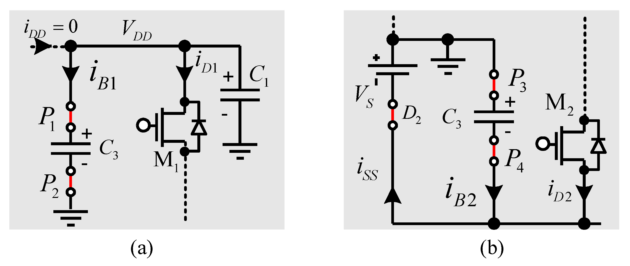
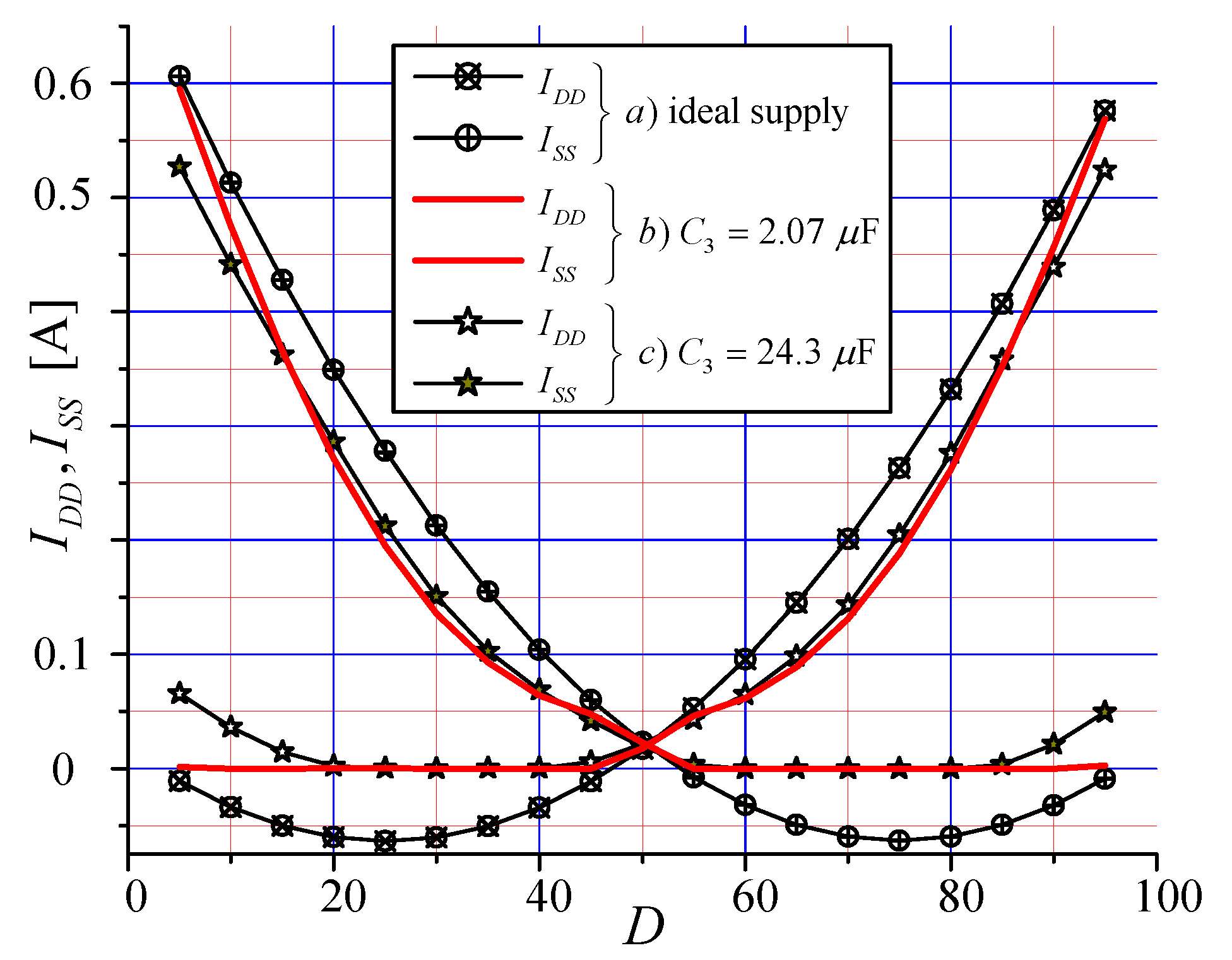
4. SC Compensation of BP Effect

SC techniques have long been routinely migrated from mixed-signal processing to power converter electronics [27,28,29,30,31,32]. With a simple rearrangement of switches, or by manipulation of frequency and phase of clock signals, SC counterparts of continuous circuits can easily acquire new features that are difficult to achieve in the continuous domain. One of the features is a flexible energy transfer from one part of the circuit to another, which is regularly used in power electronics designs [29,30,31,32].
Let us consider circuit from Figure 6, with a BP SC suppression subcircuit. The analysis is performed for 0 < D < 0.5, while the conclusions for 0.5 < D < 1 are symmetric and can be deduced from analogy. The SC subcircuit consists of capacitor C3 << C1, C2, MOS switches P1, P2, P3, and P4, and gate-drive logic (not shown on the picture). The gate-drive logic of P1, P2, P3, and P4 is clocked with a two-phase clock scheme CLK1 with nonoverlapping phases having duty factor of 0.5. The CLK1 with frequency f1 = 1/T1 is physically distinct to CLK. Clock phase φ1, which is active during the first half of switching period T1, turns on P1 and P2, while P3 and P4 are in the blocked state. During the second part of the switching period, clock phase φ2 is active, and it turns on P3 and P4, while P1 and P2 are in a blocked state. Therefore, during the first half of the period T1, capacitor C3 is connected in parallel with capacitor C1, while, during the rest of the period, it is connected in parallel with C2.

4.1. Power Efficiency Analysis

For values of D, which makes VDD greater than VS, a simplified version of the circuit, from Figure 6, is presented in Figure 7a,b. The current iDD is equal to zero, the VDD portion of the power supply is blocked, and, therefore, it is not shown. On the other hand, iSS > 0, maintaining negative supply active, and −VSS = −VS. Since capacitor C2 is at constant voltage VS, then ic2 = 0. Thus, C2 does not affect circuit operation, so it is not included in Figure 7.
Figure 7a describes the active part of the BP suppression SC circuit during the first half of the switching period T1. Switches P1 and P2, are closed, and C3 is connected in parallel with C1. C1 is large enough so that voltage VDD can be considered constant over several periods of T1. Since C3 << C1, capacitor C3 is charged to voltage VDD.
Figure 7b describes the active part of the BP suppression SC circuit during the second half of the switching period T1. Switches P3 and P4 are closed; capacitor C3 is connected to PS and charged to voltage VS.
Voltage change ΔVC3 (1) on capacitor C3, at the beginning of first half of the period T1, is equal to Δ V C 3 ( 1 ) = V D D V S , thus having the charge flowing through C3 equal to Δ Q ( 1 ) = Δ V C 3 ( 1 ) C 3 . Consequently, the average value of current iB1 during single switching period T1 is equal to
I B 1 = Δ Q ( 1 ) / T 1 = C 3 ( V D D V S ) / T 1 .
Voltage change ΔVC3 (2) on capacitor C3, at the beginning of second half of the period T1, is equal to Δ V C 3 ( 2 ) = V S V D D = Δ V C 3 ( 1 ) . Therefore, the charge flowing through C3 is equal to Δ Q ( 2 ) = Δ Q ( 1 ) , and the average value of current iB2 during single switching period T1 is equal to −IB1. According to Figure 7a, it is fulfilled that −IB1 = ID1, from which it follows that IB2 = ID1. Since ISS = IB2 + ID2, it follows that ISS = ID1 + ID2, and total power consumption is equal to Ptot = VS(ID1 + ID2). The obtained result confirms that Ptot is the same as in the ideal case and that applied SC circuit provides maximum consumption efficiency of the class-D amplifier.

4.2. BP Analysis

Based on Figure 7 and Equation (21), it can be seen that the SC circuit behaves as the circuit from Figure 5, where VDD bus is connected via SC equivalent resistor r0 = T1/C3 to the generator VDZ = VS and that IB1I01
I B 1 = V D D V S T 1 / C 3 = V D D V S r 0 = I 01 .
Therefore, for BP analysis, circuits from Figure 4 and Figure 5, together with corresponding Equations, can be used.
If we neglect I0, then V0 = VDZ = VS, α =1, and BP effect occurs for full range 0 <D < 0.5:
V D D = V S 1 + β D ( 1 D ) 1 + β D 2 > V S .
Contrary to dissipative BP suppression, SC equivalent resistor r0 can be arbitrarily small. Therefore, BP effect can be made negligible. For example, if β = 0.5, maximum voltage on VDD bus is achieved approximately at D = 1/4 and is equal to:
V D D = V S 1 + 0.5 3 / 16 1 + 0.5 1 / 16 = 1.06 V S .
In practical realizations, there is always a small current I0, which causes the current IDD to be greater than zero during a small part of the period T. Still, this fact does not change the essence of the conducted analysis.

4.3. Dynamical Behavior

Due to the existence of the zero-order hold effect, SC circuits are well equivalent to their continual counterparts up to ≈1/10 of the sampling frequency [27,28]. From that side, proposed SC compensation of BP effect is useful to at least 1/10 of f1 = 1/T1. With the current state of technology, sampling frequencies can routinely go over 50 kHz, so that blocking capacitors solve the BP problem easily at f1/10. As an illustration, we may consider the following “worst-case” example. Let us assume that the sampling frequency of the SC BP suppression circuit is f1 = 10 kHz. Thus, we can pessimistically consider that over f1/10 = 1 kHz SC circuit is ineffective regarding BP suppression. Furthermore, let us assume that class-D amplifier has the following parameters: Ra =1 Ω, and Ca = 4.7 mF. At f1/10 = fa = 1 KHz, according to Equation (1), ΔVBB/VBB = 1/(4.7∙8π) = 0.0085, which is below 1%. Therefore, if usual switching frequencies are used, modeling performed in the paper is sufficient for accurate prediction of the dynamical behavior of the proposed SC BP suppression method.
When frequencies below f1/10 are observed, the transient behavior of the voltages vDD and vSS is defined by the time constants τDD = r0C1 and τSS = r0C2. For the case of positive supply bus, when diode D1 is blocked, and RB is disconnected, as in Figure 6, Unit-step response of the voltage vDD is in the form
S D D ( t ) = 1   [ A ]   r 0 ( 1 e t / τ D D ) u ( t ) ,
where u(t) is Unit-step function, and assumed excitation is current iD1. The same equation is valid for a negative supply bus. It can be seen that the worst case is on DC and that the purpose of the dynamic behavior analysis can only be to optimize the values of the blocking capacitors C1 and C2.

4.4. Experimental Verification

Previous derivations regarding power consumption and suppression of BP effect are verified using experimental setup based on Figure 6. Power source PS is configured as ±12 V desktop power supply modified with diodes D1 and D2 (MUR1045), which gives final output voltage as ±VS ≈ ±11.5 V at 0.5 A load and load regulation of 0.6 V/A. When needed, the bilateral power supply is simulated by adding a blinder resistor RB = 215 Ω between nodes A and B, as in Figure 6, so that currents IDD and ISS could flow in both directions. The current through RB has a negligible effect on the load regulation; it does not affect IDD or ISS and is not covered by the measurements. Measured electrical quantities are IDD, ISS, VDD, VSS, and IL in a range of 0.05 < D < 0.95. For each pair of MOS transistors, and an accompanying gate driving logic, one-half of each of the three different L6202 is used. Capacitors C1 and C2 have values of 1000 μF. Quiescent supply current for D = 0.5 is I0 ≈ 20 mA, giving power consumption at rest as
P 0 = 2 V S I 0 = 460   mW .
Used load is made of coil with L = 50 mH, rL = 5.3 Ω, and resistor RL = 10 Ω, which gives R = RL + rL = 15.3 Ω. Switching periods are T1 = T = 100 μs. For a set of different C3 values, the calculated characteristic quantities, used in paper equations, are given in Table 1. VDD supply bus voltage is calculated for D = 1/4, which is near the extreme value for both VDD and VSS.
Measured supply voltages VDD and VSS for the selected set of C3 values, as well as calculated supply voltages based on Table 1, are given in Figure 8. Measured voltages are presented as line charts, whereas calculated voltages are presented as symbol + line charts. The picture shows a good agreement between experiment and theory.
Measured supply currents IDD and ISS against D, are presented in Figure 9. For cases (b) and (c), supply currents are greater than or equal to zero for a complete range of D, whereas sum IDD + ISS is the same for all 3 cases, which corroborates theoretical predictions.
Power consumption, for several measured or theoretically calculated cases, is presented in Figure 10. For cases (b) and (c), power supply is unidirectional, and the SC circuit is fully active. For the case (a) in which power supply is bilateral, capacitor C3 is removed (C3 = 0) so that SC circuit contributes to quiescent consumption, but it does not engage in BP suppression.
When power consumption is measured, for cases (a), (b), and (c), it is done indirectly as
P t o t = V D D I D D + V S S I S S .
For the case (d) and (e), power consumption is calculated on the basis of Equation (8) and Equation (10), augmented with quiescent consumption P0:
P t o t = P o + R I L M 2 ( 1 2 D ) 2 ,
for bilateral power supply, and
P t o t = { P 0 + R I L M 2 ( 1 D ) ( 1 2 D ) ,   D < 0.5 P 0 + R 0 I L M 2 D ( 1 2 D ) ,   D > 0.5 ,
for unilateral power supply.
It can be observed that the use of proposed SC circuit preserves energy efficiency, as in the case of ideal power supply.
The waveforms for illustrating dynamic behavior of the positive and negative supply voltages when the duty factor alternately changes from 0.5 to 0.25, and vice versa, with intervals of 50 ms, are shown in Figure 11. Responses are captured in a following way: for the case of bilateral supply, case (a); for the case of unilateral power supply and two different values of capacitor C3, cases (b), (c). Voltage vL, a seen in Figure 6, is displayed on channel CH 1, voltage +vDD is displayed on channels CH 5–CH 7, and voltage −vSS is displayed on channels CH 2–CH 4.
For the case (a), there is no bus-pumping, and power supply voltages +vDD and −vSS suffer from voltage drops caused by load regulation. Transient response of supply voltages follows the transient response of the load, with time constant τL = L/R = 3.3 ms.
For the cases (b) and (c), only positive portion of the power supply is blocked during time periods when D = 0.25, and +vDD bus experiences BP. Transient response of +vDD is slowed down due to time constants τ3 and τ4, Table 1. On the other hand, the negative portion of the power supply is active, and transient response of the voltage −vSS follows transient response of the load, according to time constant τL.

5. Conclusions

For the case of standard unilateral power supplies, described dissipative methods for BP suppression in class-D amplifiers can be extremely simple and cost-effective. Still, they cannot provide the full potential of HB topology regarding power efficiency. As an alternative, a high-efficiency SC technique for BP reduction in HB class-D amplifiers is proposed in this paper. It is shown that the proposed SC technique can reduce BP significantly and preserve energy efficiency of ideal HB class-D amplifier, with advantages of high efficiency, simple implementation possibility, and low cost. Analytical results are given to verify the operation principles. Hardware implementation of the proposed technique and its operation considerations were analyzed and described. A laboratory prototype was implemented and tested to show its performance, regarding BP suppression, power efficiency, and dynamical characteristics.

Author Contributions

Conceptualization, M.P. and S.M.; methodology, M.P.; validation, M.P., and S.M.; formal analysis, S.M.; resources, M.P.; writing—original draft preparation, M.P.; writing—review and editing, M.P. and S.M.; supervision, S.M. All authors have read and agreed to the published version of the manuscript.

Funding

This research received no external funding.

Acknowledgments

This work was supported by bilateral scientific cooperation between the Ministry of Education, Science and Technology Development of the Republic of Serbia and the Ministry of Science of the Republic of Montenegro: Projects 451-03-02263/2018-09/1 and 451-03-02263/2018-09/14.

Conflicts of Interest

The authors declare no conflict of interest.

Nomenclature

DC and average quantities are represented by uppercase symbols with uppercase subscripts, for example, ID1. AC quantities are represented by lowercase symbols with lowercase subscripts, for example, id1. Total quantities AC+DC are characterized by lowercase symbols with uppercase subscripts, for example, iD1 = id1 + ID1. Any quantity is considered negative if it is less than zero; for example, negative iD1 means that iD1 < 0.

References

  1. Honda, J.; Adams, J. Class D Audio Amplifier Basics, Application Note AN-1071. International Rectifier (USA). February 2005. Available online: https://www.infineon.com/dgdl/an-1071.pdf (accessed on 2 November 2020).
  2. Zia, M.Y.I.; Tierno, R.; Luque-Nieto, M.-Á.; Otero, P. An Energy-Efficient Integration of a Digital Modulator and a Class-D Amplifier. Electronics 2020, 9, 1319. [Google Scholar] [CrossRef]
  3. Colli-Menchi, A.I.; Sánchez-Sinencio, E. A High-Efficiency Self-Oscillating Class-D Amplifier for Piezoelectric Speakers. IEEE Trans. Power Electron. 2015, 30, 5125–5135. [Google Scholar] [CrossRef]
  4. Galic, J.; Pesic-Brdjanin, T.; Iriskic, L. Class-D Audio Amplifier using PulseWidth Modulation. In Proceedings of the 6th Small Systems Simulation Symposium 2016, Nis, Serbia, 12–14 February 2016; pp. 133–136. [Google Scholar]
  5. Kovacevic, S.; Pesic-Brdjanin, T.; Galic, J. Class D Audio Amplifier with Reduced Distortion. In Proceedings of the 2018 International Symposium on Industrial Electronics (INDEL), Banja Luka, Bosnia, Herzegovina, 1–3 November 2018; pp. 1–4. [Google Scholar]
  6. Zaman, H.; Zheng, X.; Wu, X.; Khan, S.; Ali, H.A. Fixed-Frequency Sliding-Mode Controller for Fourth-Order Class-D Amplifier. Electronics 2018, 7, 261. [Google Scholar] [CrossRef] [Green Version]
  7. Zhou, X.; Xu, J.; Zhong, S.; Liu, Y. Soft Switching Symmetric Bipolar Outputs DC-Transformer (DCX) for Eliminating Power Supply Pumping of Half-Bridge Class-D Audio Amplifier. IEEE Tran. Power Electron. 2019, 34, 6440–6455. [Google Scholar] [CrossRef]
  8. Zhong, S.; Xu, J.; Zhou, X. 2.1-Channel Switching Amplifier With DC/High-Frequency-AC Mixed Power Supply for Efficiency Improvement and Bus Voltage Pumping Elimination. IEEE Tran. Power Electron. 2018, 33, 9110–9115. [Google Scholar] [CrossRef]
  9. Zhang, G.; Chen, H.; Qu, L.; Chen, S.; Zhang, Y. A Family of Y-Impedance-Network Half-Bridge Converters with Additional Voltage Adjustment Function. Energies 2019, 12, 3430. [Google Scholar] [CrossRef] [Green Version]
  10. Wei, Y.; Xu, Y.; Zou, J.; Li, Y. Current Limit Strategy for BLDC Motor Drive With Minimized DC-Link Capacitor. IEEE Tran. Ind. Appl. 2015, 51, 3907–3913. [Google Scholar] [CrossRef]
  11. Erickson, R.W.; Maksimovic, D. Fundamentals of Power Electronics, 2nd ed.; Kluwer Academic Publishers: Secaucus, NJ, USA, 2001. [Google Scholar]
  12. Roinila, T.; Vilkko, M.; Sun, J. Online Grid Impedance Measurement Using Discrete-Interval Binary Sequence Injection. IEEE J. Emerg. Sel. Top. Power Electron. 2014, 2, 985–993. [Google Scholar] [CrossRef]
  13. Miao, Z.; Tong, H.; Yao, W.; Lu, Z. Online high-band grid impedance measurement using variable frequency carrier-based PWM scheme. CSEE J. Power Energy Systems 2020. [Google Scholar] [CrossRef]
  14. Velasco-Quesada, G.; Román-Lumbreras, M.; Conesa-Roca, A.; Jerez, P. Design of a Low-Consumption Fluxgate Transducer for High-Current Measurement Applications. IEEE Sens. J. 2011, 11, 280–287. [Google Scholar] [CrossRef]
  15. Veinovic, S.; Ponjavic, M.; Milic, S.; Djuric, R. Low-power design for DC current transformer using class-D compensating amplifier. IET Circuits Devices Syst. 2018, 12, 215–220. [Google Scholar] [CrossRef]
  16. Ponjavic, M.; Veinovic, S. Low-power self-oscillating fluxgate current sensor based on Mn-Zn ferrite cores. J. Magn. Magn. Mater. 2021, 518. [Google Scholar] [CrossRef]
  17. Radivoje, D.; Ponjavic, M. Self-oscillating fluxgate current sensor with pulse width modulated feedback. Electronics 2010, 14, 33–36. Available online: http://els-journal.etf.unibl.org/journal/Vol14No2/xPaper_06.pdf (accessed on 19 December 2020).
  18. Berkhout, M. An integrated 200-W class-D audio amplifier. IEEE J. Solid State Circuits 2003, 38, 1198–1206. [Google Scholar] [CrossRef]
  19. 7 IRAUDAMP4: 120 W x 2 Channel Class D Audio Power Amplifier Using IRS20955 and IRF6645. Available online: https://www.infineon.com (accessed on 19 December 2020).
  20. Leigh, S.P.; Mellor, P.H.; Cheetham, B.M.G. Distortion analysis and reduction in a completely digital PWM Class-D power amplifier. Int. J. Model. Simul. 1994, 14, 75–79. [Google Scholar] [CrossRef]
  21. Bai, M.R.; Lee, D.J. Comparison of active noise control structures in the presence of acoustical feedback by using H∞ synthesis techniques. J. Sound Vib. 1997, 206, 453–471. [Google Scholar] [CrossRef] [Green Version]
  22. Sala, V.; Romeral, L.; Garcia, T.; Delgado, M. Study of hybrid active control strategies for the BP cancellation in the Half-Bridge Class-D audio power amplifiers. In Proceedings of the 2011 IEEE International Symposium on Industrial Electronics, Gdansk, Poland, 27–30 June 2011; pp. 431–437. [Google Scholar] [CrossRef]
  23. Sala, V.M.; Cusido, J.; Delgado, M.; Ruiz, G.; Ortega, J.A. Feed-Back Active Control for Half-Bridge Class-D audio amplifiers. In Proceedings of the 2008 IEEE International Symposium on Industrial Electronics, Cambridge, UK, 30 June–2 July 2008; pp. 369–373. [Google Scholar] [CrossRef]
  24. Ljusev, P.; Andersen, M.A.E. Direct-conversion Switching-mode Audio Power Amplifier with Active Capacitive Voltage Clamp. In Proceedings of the 2005 IEEE 36th Power Electronics Specialists Conference, Recife, Brazil, 16 June 2005; pp. 2848–2854. [Google Scholar] [CrossRef] [Green Version]
  25. Hoyerby, M.C.W.; Andersen, M.A.E. Carrier Distortion in Hysteretic Self-Oscillating Class-D Audio Power Amplifiers: Analysis and Optimization. IEEE Trans. Power Electron. 2009, 24, 714–729. [Google Scholar] [CrossRef] [Green Version]
  26. Xu, D.; Zhou, G.; Huang, R.; Liu, X.; Liu, F. High Efficiency Half Bridge Class-D Audio Amplifier System With Front-End Symmetric Bipolar Outputs LLC Converter. IEEE Trans. Ind. Electron. 2020, 68, 1220–1230. [Google Scholar] [CrossRef]
  27. Allen, P.E.; Sánchez-Sinencio, E. Switched Capacitor Circuits; Van Nostrand: New York, NY, USA, 1984. [Google Scholar]
  28. Liou, M.; Kuo, Y.-L. Exact analysis of switched capacitor circuits with arbitrary inputs. IEEE Trans. Circuits Syst. 1979, 26, 213–223. [Google Scholar] [CrossRef]
  29. Daowd, M.; Antoine, M.; Omar, N.; van den Bossche, P.; van Mierlo, J. Single Switched Capacitor Battery Balancing System Enhancements. Energies 2013, 6, 2149–2174. [Google Scholar] [CrossRef] [Green Version]
  30. Ye, Y.; Cheng, K.W.E.; Fong, Y.C.; Xue, X.; Lin, J. Topology, Modeling, and Design of Switched-Capacitor-Based Cell Balancing Systems and Their Balancing Exploration. IEEE Tran. Power Electron. 2017, 32, 4444–4454. [Google Scholar] [CrossRef]
  31. Ahmadi, D.; Zou, K.; Li, C.; Huang, Y.; Wang, J. A Universal Selective Harmonic Elimination Method for High-Power Inverters. IEEE Trans. Power Electron. 2011, 26, 2743–2752. [Google Scholar] [CrossRef]
  32. Tang, S.T.S.; Wang, J.; Zheng, R.; Wang, D.; Zhang, C.; Yin, X.; Shuai, Z.; Shen, J. Detection and Identification of Power Switch Failures Using Discrete Fourier Transform for DC-DC Flying Capacitor Buck Converters. IEEE J. Emerg. Sel. Top. Power Electron. 2020. [Google Scholar] [CrossRef]
Figure 1. Basic configuration of class-D half-bridge (HB) amplifier without control circuitry. Amplifier output stage is powered by symmetrical supply with voltages VDD = VS and −VSS = −VS.
Electronics 09 02197 g001
Figure 2. Normalized values ID1/ILM and ID2/ILM with respect to D.
Electronics 09 02197 g002
Figure 3. Normalized power consumption as a function of D, for several amplifier realizations: (a) HB with bilateral power supply, Equation (8); (b) Class-AB power amplifier, Equation (9); (c) HB with unilateral power supply and ideal absorption of negative supply currents, Equation (10); (d) Ptot1 Equation (19); (e) Ptot2 Equation (20).
Electronics 09 02197 g003
Figure 4. Principal schematic of class-D HB amplifier without control circuitry. An amplifier is powered with unidirectional power supply and augmented with pus-pumping suppression electronics. Capacitors C1 and C2 are large enough so that voltages on supply busses can be considered as ripple-free.
Electronics 09 02197 g004
Figure 5. Equivalent representation of subcircuits U1 and U2. Typically, voltage source VDZ is made of Zener diode with breakdown voltage VDZ. Subcircuits U1 and U2 consume energy and, therefore, are thermodynamically passive.
Electronics 09 02197 g005
Figure 6. Principal schematic of class-D HB amplifier without control circuitry. The amplifier is powered with unidirectional power supply and augmented with bus-pumping (BP) switched-capacitor (SC) suppression circuit. Resistor RB is disconnected during regular operation of the amplifier. The total resistance R is the sum of the coil resistance rL and the load resistance RL: R = RL + rL.
Electronics 09 02197 g006
Figure 7. The active part of the BP suppression SC circuit: (a) during the first half of switching period T1; (b) during the second half of the switching period T1.
Electronics 09 02197 g007
Figure 8. Measured and calculated supply voltages VDD and VSS for the selected set of C3 values. Measured voltages are presented as line charts, whereas calculated voltages are presented as symbol + line charts.
Electronics 09 02197 g008
Figure 9. Measured supply currents: (a) ideal (bilateral) power supply; (b) unilateral power supply and C3 = 2.07 μF; (c) unidirectional power supply and C3 = 24.3 μF.
Electronics 09 02197 g009
Figure 10. Measured and calculated power consumption: (a) measured, bilateral power supply; (b) measured, unidirectional supply and C3 = 2.07 μF; (c) measured, unidirectional supply and C3 = 24.3 μF; (d) calculated, ideal case augmented with quiescent consumption P0 (e) calculated, unilateral power supply and perfect absorption of negative supply currents, raised with quiescent consumption P0 (ideal dissipative method).
Electronics 09 02197 g010
Figure 11. Vertical scale CH 1: 2 V/div, zero position −4 V. Vertical scale CH 2–CH 4: 200 mV/div, zero position 12.5 V. Vertical scale CH 5–CH 7: 200 mV/div, zero position −12.2 V. Horizontal scale: 10 ms/div. Channels: (a) CH 2 and CH 7, transients on supply busses, bidirectional power supply; (b) CH 6 and CH 3, transients on supply busses, unidirectional power supply, C3 = 24.3 μF; (c) CH 6 and CH 3, transients on supply busses, unidirectional power supply, C3 = 24.3 μF. (d) CH 5 and CH 4, transients on supply busses, unidirectional power supply, C3 = 10.3 μF.
Electronics 09 02197 g011
Table 1. Characteristic quantities r0, V0, α, β, and extreme values for VDD and VSS.
C3
[μF]
r0 = T1/C3 [Ω]V0 = VSI0r0 [V]αβMax{VDD} at D = 1/4, Equation (15)
Max{VSS} at D = 3/4
[V]
Time
Constant
C1r0 [ms]
2.0748.310.530.9163.15714.48τ1 = 48.3
5.1619.411.110.9661.26712.83τ2 = 19.4
10.39.711.310.9830.63512.19τ3 = 9.7
24.34.111.420.9930.26911.80τ4 = 4.1
Publisher’s Note: MDPI stays neutral with regard to jurisdictional claims in published maps and institutional affiliations.

