Article

A New Hybrid Ćuk DC-DC Converter with Coupled Inductors

Applied Electronics Department, Politehnica University Timișoara, 300006 Timisoara, Romania
*
Author to whom correspondence should be addressed.
Electronics 2020, 9(12), 2188; https://doi.org/10.3390/electronics9122188
Submission received: 16 November 2020 / Revised: 14 December 2020 / Accepted: 15 December 2020 / Published: 18 December 2020
(This article belongs to the Section Power Electronics)

Abstract

:
This paper proposes a new hybrid Ćuk-type converter employing two inductors built on the same core which can be successfully used in applications requiring an output voltage considering higher than the input one. With few components added, in the proposed converter the static conversion ratio can be easily extended becoming wider compared to the classical Ćuk topology. At the same duty cycle range the output voltage is higher than in the classical Ćuk converter. The output voltage remains with negative polarity and with a reduced ripple. An advantage of the new converter is given by its two degrees of freedom. A DC and AC analysis is carried out, device stresses are evaluated and a comparative analysis of the proposed hybrid Ćuk topology to other indirect converters has also been performed. All the equations necessary for designing the converter are provided. The simulations performed together with the practical experiments carried out, all results confirm that the theoretical considerations are correct and validate the features that the proposed converter can provide a higher static conversion ratio without operating at high duty cycles.

1. Introduction

Dc-dc converters are used in a large variety of applications: unidirectional and bidirectional chargers in automotive, renewable energies in photovoltaic cells for example, dc grids, cellphones, computers, laptops and so forth. These power circuits should be able to step-up [1,2,3,4,5,6,7,8,9], step-down [10,11,12,13] or step-up/step-down [14,15,16,17,18,19,20,21] the voltage from the input. The polarity of the output voltage can be the same [1,2,3,4,6,7,8] or reverse [5,22,23,24,25,26,27,28,29] compared to that of the input voltage. Regarding to the static conversion ratio, the converter can be used in applications where a small or large difference between the input and output voltages of the converter are encountered. Therefore, depending on the application requirements, considering the few parameters mentioned before, different types of converters exist on the market. Because this paper introduces a new Ćuk topology, different types of both step-down/step-up converters have been analyzed [14,15,16,17,18,19,20,21,22,23,24,25,26,27,28,29,30,31,32]. If isolation is not necessary, the classical Buck-Boost converter [30] can be used. It even has the advantage of a reduced number of components and simplicity; however, control is sometimes difficult because its transistor is floating. Another step-up/step-down structure it is the classical Ćuk converter [32]. This topology can be used with coupled [32] or uncoupled inductors [31]. The advantage of coupling the inductors is that the current through the one of the inductors can be made with a very small ripple. For increasing the step-down nature of the converter, the authors of References [25,27], are using a switched-capacitor or switched inductor structure [25,27] that it is inserted in the traditional Ćuk converter. The same work reported in References [25,27] improve the step-up capabilities by inserting a switched inductor structure in the classical Ćuk converter. In References [24,28], it is shown that coupling the inductors in the additional switching cell inserted in a Ćuk converter, this leads to a higher step-up conversion ratio than in the classical one. Different structures of isolated Ćuk converters are presented in References [33,34]. The step-up and step-down nature can be also found in quadratic converters [20].
How it was mentioned, in this paper a new hybrid Ćuk-type topology with coupled inductors exhibiting a higher static conversion ratio than in a classical Ćuk converter is introduced. The development of the new proposed converter, dc analysis and the main waveforms are depicted in Section 2. The semiconductors current and voltage stresses, the peak-to-peak ripples and the Continuous Conduction Mode (CCM) operation condition are derived in Section 3. In Section 4 a theoretical comparative study to other step-up/step-down topologies is performed and a design example is presented in Section 5.
In order to confirm the theoretical considerations at set of simulations are performed in Section 6. Finally, the practical experiments that validate the feasibility of the proposed converter are presented in Section 7, while Section 8 is devoted to the conclusions.

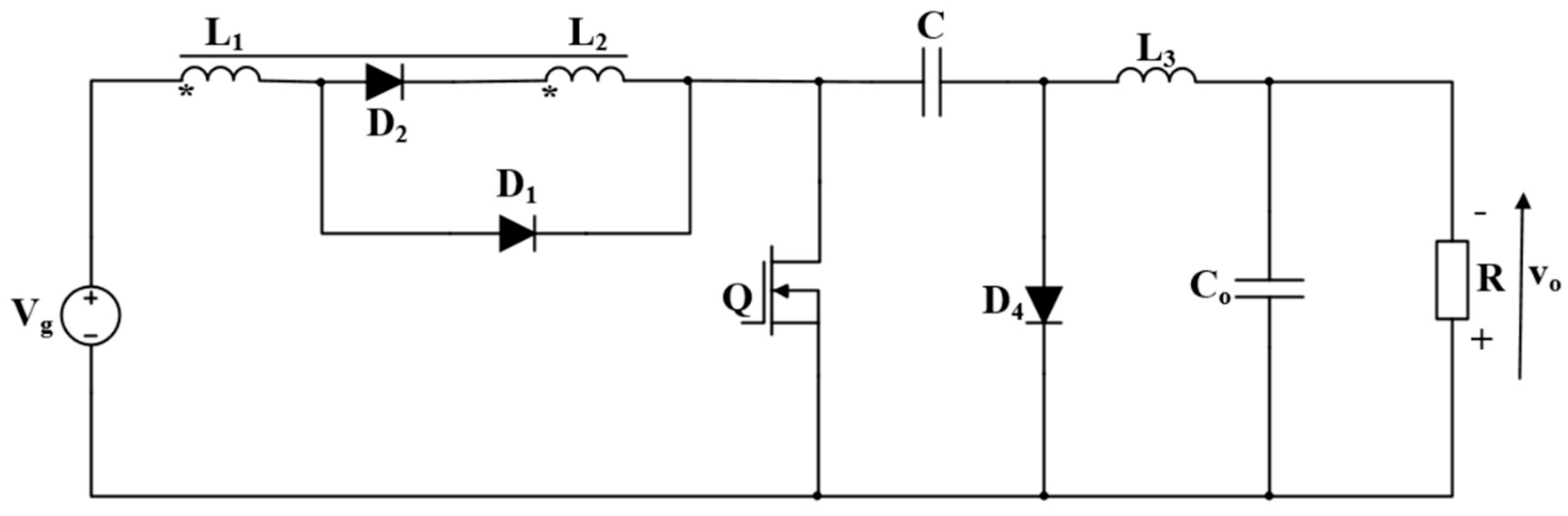
2. Description of Operation and Steady State Analysis of the Proposed Hybrid Ćuk Converter

The origin of the new proposed converter is the hybrid step-up converter with switching structure Up3 from Reference [25], enfaced in Figure 1.
The first step in developing the proposed converter was to couple the inductors L1 and L2. Assuming perfect coupling and denoting by N1 and N2 the turns number corresponding to L1 and L2 respectively, the transformer ratio n is assumed higher than unity.
The transformer ratio is defined as:
n = N 2 N 1 > 1 .
For n > 1, diode D3 will be always off and therefore it can be removed from the circuit.
The new proposed converter, as Figure 2 reveals includes one transistor, three diodes, three inductors out of which two are coupled, therefore two magnetic cores are used and two capacitors.
Modelling the coupled inductors by an ideal transformer (IT) together with a magnetizing inductor, LM, the equivalent schematic is represented in Figure 3. In this approach the magnetizing inductor LM is considered equal with L1 and all components are assumed to be ideal.
In Continuous Conduction Mode (CCM), depending on the state of the power transistor, two topological states are possible. The switching frequency and the corresponding switching period are denoted fs and Ts respectively. The converter is controlled by a pulse width modulated signal of duty cycle D. The first topological state, last from 0 to D∙Ts and the configured circuits is presented in Figure 4a, where transistor Q and diode D1 are on, while the other two diodes D2 and D4 are off, as they are reversely biased. From D∙Ts to Ts, the second topological state is configured with transistor Q and diode D1 off, while diodes D2 and D4 are on. The corresponding circuit is depicted in Figure 4b.
Taking into consideration the notations from Figure 3, the ideal transformer equations are:
{ v 1 1 = v 2 n   i 1 + n · i 2 = 0
The small ripple assumptions is assumed for the capacitor voltages and inductor currents, therefore in the subsequent analysis these variable are assumed constant and equal to their dc value.
Invoking the volt-second balance principle for the magnetizing inductor LM and inductor L3, the equations are:
{ D · V g + ( 1 D ) · V g V C 1 + n = 0 D · ( V C V C O ) + ( 1 D ) · ( V C O ) = 0
After solving system (3), the dc voltages across the internal capacitor C and across the output capacitor CO can be written as:
V C = 1 + n · D 1 D · V g .
V C O = ( 1 + n · D ) · D 1 D · V g .
As V C O = V O , the ideal static conversion ratio M of the new converter is given by (5):
M = ( 1 + n · D ) · D 1 D .
From (6), the duty cycle can be expressed in terms of static conversion ratio as:
D = 1 M + ( 1 + M ) 2 + 4 n M 2 n .
Examining the Equation (6), after some simple algebra, it follows that if the duty cycle is higher than 1 + n 1 n the static conversion ratio is higher than unity. For n = 2, we have 1 + n 1 n = 0.365 , for n = 3, 1 + n 1 n = 0.33 , which means that the proposed converter from Figure 2 has a both step-up and step-down nature. However, compared to the Buck-Boost or the Ćuk converter the converter starts to step-up as a considerably lower duty cycle, in the example provided around 0.33 compared to the value of 0.5. The higher the value of n the lower will be the duty cycle that defines the step-up region. In conclusion, the step-up region is more extended compared to the Buck-Boost and the Ćuk converter.
For calculating the dc magnetizing inductor current ILM and the dc output inductor current IL3, the charge balance principle related to the capacitor C and CO is invoked:
{ D · ( I L 3 ) + ( 1 D ) · I L M 1 + n = 0 D · ( I L 3 V C O R ) + ( 1 D ) · ( I L 3 V C O R ) = 0
Solving (8) the dc magnetizing inductor current ILM is:
I L M = D 2 · ( 1 + n · D ) · ( 1 + n ) ( 1 D ) 2 · V g R .
and, the dc output inductor current IL3 is:
I L 3 = D · ( 1 + n · D ) 1 D · V g R .
The steady state waveforms for the reactive components and semiconductor devices are drawn in Figure 5, Figure 6 and Figure 7.
The control voltage q(t) associated to the transistor is chosen as a reference, where q(t) is given by:
q ( t ) = { 1 ,   Q O N 0 ,   Q O F F .
Because the inductive voltages are piecewise constant, exhibiting a rectangular shape, the inductive currents will be piecewise linear, increasing if the voltage is positive and decreasing if the voltage is negative. Similarly, the internal capacitor current is piecewise constant, resulting in a piecewise linear internal capacitor voltage. As the output node is a non-switched one, the current through the output capacitance, Co, is piecewise linear - has the same shape as iL3 but with zero dc value. Since the current of the capacitance Co is piecewise linear, its voltage will be piecewise parabolic.

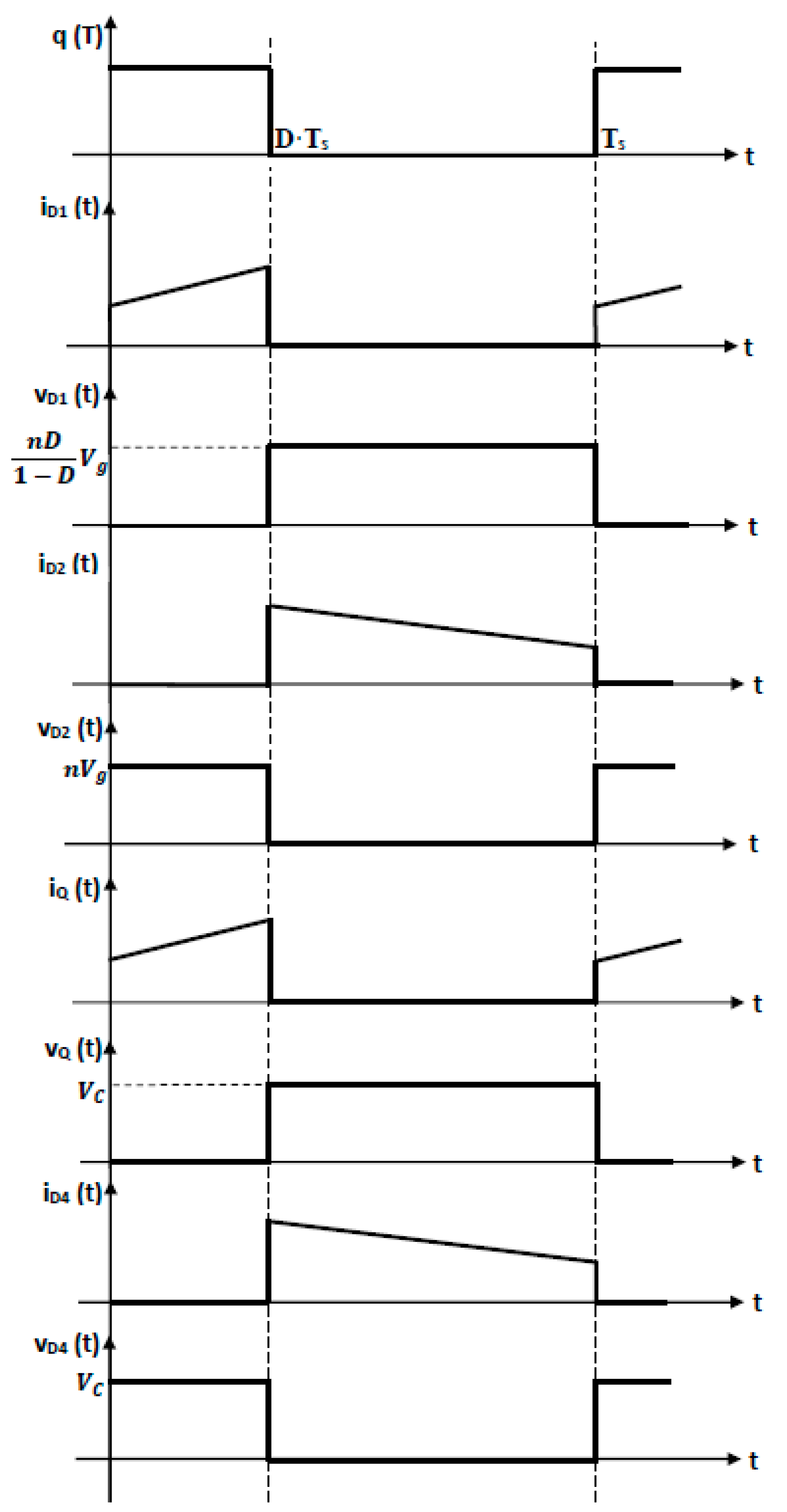
3. Semiconductor Stresses and Inductor Currents and Capacitor Voltages Peak-to-Peak Ripple

In the design process of the converter and practical implementation is necessary that the current and voltage stresses related to the semiconductors to be known. These stresses will be expressed in terms of the supply voltage Vg, the control duty cycle D, load R and the circuit parameters.
The voltage across switch Q is calculated from the second topological state as being equal to the voltage across the internal capacitor VC. By replacing Vc from (4), the transistor voltage stress is:
V Q = 1 + n · D 1 D · V g .
The dc transistor current stress is the sum between ILM and IL3, so the dc transistor current is:
I Q = D · ( I L M + I L 3 ) = D 2 · ( 1 + n · D ) 2 ( 1 D ) 2 · V g R .
The voltage stress across diode D1 results from second topological state:
V D 1 = n · V g V C 1 + n = n · D 1 D · V g .
The dc current through diode D1 is given by:
I D 1 = D · I L M = D 2 · ( 1 + n · D ) · ( 1 + n ) ( 1 D ) 2 · V g R .
The voltage across diode D2 can be found from first topological state:
V D 2 = n · V g .
The dc current through the diode D2 is calculated as:
I D 2 = ( 1 D ) · I L M 1 + n = D 2 · ( 1 + n · D ) 1 D · V g R .
The voltage across diode D4 can be found from first topological state:
V D 4 = 1 + n · D 1 D · V g .
The dc current through diode D4 can be written as:
I D 4 = ( 1 D ) · ( I L M 1 + n + I L 3 ) = D · ( 1 + n · D ) 1 D · V g R .
Regarding the ripples, the magnetizing peak-to-peak current ripple is given by:
Δ I L M = D · V g L M · f s .
The peak-to-peak current ripple for L3 inductor can be expressed as:
Δ I L 3 = D · ( 1 + n · D ) · V g L 3 · f s .
The internal capacitor voltage ripple, Δ V C , is provided by:
Δ V C = D 2 · ( 1 + n · D ) 1 D · V g C · R · f s .
In order to calculate the output capacitor voltage ripple, the same technique applied for the Buck converter output voltage ripple calculations is used. The charge injected in the capacitor between the time moments corresponded to the minimum and the maximum capacitor voltage is:
Δ Q = 1 2 · T s 2 · Δ I L 3 2 .
Now, the capacitor voltage ripple can be easily estimated as:
Δ V C O = Δ V O = Δ Q C .
The CCM operation condition requires the diodes to be permanently on during the whole topological state they are assumed to conduct. This imposes the condition that diode currents have to stay positive during those topological states or equivalently the minimum current to be positive.
Because D1 and D2 currents are equal to iLM for these diodes the CCM condition is the same and imposes that the minimum magnetizing current, ILMmin to be positive. As, I L M m i n = I L M 1 2 · Δ I L M , using (9) and (20), the final condition is:
2 · L M · f s R ( 1 D ) 2 D · ( 1 + n · D ) · ( 1 + n ) .
The CCM condition for diode D4 takes into account the current flowing through it is i L M n + 1 + i L 3 . Because iLM and iL3 have the same monotonicity, the CCM condition results immediately.
2 · L e · f s R ( 1 D ) 2 1 + n · D ,
where, the equivalent inductor is:
L e = ( L M · ( 1 + n · D ) ) | |   L 3 1 + n .
It can be remarked that (26) has the same form to that of Buck-Boost or Ćuk converter.
Although the inductors can be designed from the CCM operation conditions, a more realistic design comes from the small ripples condition. It is known that this small ripple conditions imposes the peak-to-peak current ripple to be less than 25% of the dc value of the corresponding inductor current:
Δ I L M 1 4 · I L M
Δ I L 3 1 4 · I L 3 .
From Equations (9), (10), (20) and (21) the minimum inductor values results:
L M m i n = 4 M · ( 1 + n ) · R f s · ( 1 D )
L 3 m i n = 4 · ( 1 D ) · R f s .
Similarly, the minimum capacitor values result also from the small ripple conditions that in this case requires the capacitor voltage ripple to be less than a percent of its dc value. Using (4) and (22) the minimum required value is:
C m i n = D 2 · ( 1 + n · D ) 1 D · V g Δ V C · f s · R .
The output capacitor is design such that to be high enough to assure an output voltage ripple less than the value imposed by specifications. From Equations (5) and (24) its minimum value is given by:
C O m i n = 1 D 8 · f s 2 · L 3 · V C O Δ V C O .

4. Comparison to Similar Converter Topologies

A comparison between the proposed hybrid Ćuk dc-dc converter and different step-up/step-down topologies namely the classical Buck-Boost [30], classical Ćuk [32] and hybrid Ćuk from Reference [24] is presented in Table 1. In order the comparison to be fair, it is considered that they are supplied by the same input voltage Vg, they deliver the same output voltage Vo on the same load R. Hence, the conversion ratio M and the output power Po are the same. The comparative parameters are: the number of active and passive semiconductors, total number of components, the system order, the expression of the static conversion ratio M, the expression of the duty cycle D, the current and voltage semiconductor stresses.
From Table 1, it can be seen that each topology has only one transistor. In comparison to the classical Ćuk, the proposed topology has two additional diodes, the same system order but smaller transistor and diode dc current stresses. How it was demonstrated in Section 2, at the same duty cycle D, the static conversion ratio of the proposed topology is higher than that of any of the compared converters. This is revealed in Figure 8, where the dependency of the static conversion ratios against duty cycle for classical Ćuk and the proposed topology, at different transformer ratios, is presented. Therefore, for step-up applications where a big difference between the input and output voltage is needed the proposed hybrid Ćuk topology is better suitable.

5. Design Example

It is desired to design a hybrid Ćuk converter according to the following specifications:
  • Input voltage: Vg = 24 ÷ 36 V
  • Output voltage: Vo = 120 V
  • Output power: Po = 30 ÷ 50 W
  • Switching frequency: fs = 100 kHz
It is assumed that operation is in closed loop size that the output voltage is maintained constant.
Because the input and output voltages are known, the maximum and minimum value of the static conversion ratio can be calculated:
M m i n = V O V g m a x = 3.33
M m a x = V O V g m i n = 5 .
We shall choose to operate at a moderate duty cycle range D ∈ [0.6, 0.7].
With Dmin = 0.6, because the minimum static conversion ratio corresponds to Dmin, the necessary turns ratio results from Equations (6) and (34):
n = M m i n M m i n · D m i n D m i n D m i n 2 = 2.03 .
From Equations (7), the maximum duty cycle, that corresponds to maximum static conversion ratio is:
D m a x = 1 M m a x + ( 1 + M m a x ) 2 + 4 n M m a x 2 n = 0.68 .
The minimum and the maximum load resistor results from the maximum and the minimum output power.
R m i n = V O 2 P O m a x = 288
R m a x = V O 2 P O m i n = 480 .
The minimum value of the magnetizing inductor was calculated from Equation (30) in the worst case, that is for maximum load resistor and maximum input voltage L M m i n = 492.9   µ H was obtained. The value of L1 will be equal to the value of LM, so L1min= LMmin = 492.9 μH and L2min = n2·LMmin = 2.03 mH. For practical implementation, a value of L M = 773.38   µ H was used. From (31) the minimum value for inductor L3 is obtained for maximum input voltage and minimum output power. It results L 3 m i n = 3.1   m H and L3 = 3.45 mH was used.
The value of the internal capacitor can be calculated from (32), imposing that the voltage ripple to be less than 5% of its dc value. A minimum value of C m i n = 24.4   µ F , results. A standard value of 33   µ F is chosen. For the output capacitor the ripple is considered 10% of its dc value and from (33) a value of C O m i n = 2.08   µ F is calculated. In this case a standard value of 3.3   µ F is chosen.
The transistor voltage stress will be VQ = 210 V, according to (12) and its average current using (13) is IQ = 1.5 A. respectively. To evaluate the voltage and current stresses across the diodes, Equations (14)–(19) will be used. The highest stresses for diodes are VD = 210 V calculated from (18) and the maximum dc current ID = 1.2 A, given by (15).

6. Simulation Results

In order to check the validity of the theoretical considerations in case of the ideal hybrid Ćuk converter, a set of simulation in Caspoc [35] tool were performed. Converter parameters were the same values used for implementing the practical prototype according with the previous design specifications:
Vg = 35 V, L1 = 773.38 μH, L2 = 2.39 mH, L3 = 3.45 mH, C = 33 µF, C0 = 3.3 µF, R = 360 Ω, fs = 100 kHz.
Since the inductors were practically realized, a small change to the initial value of transformer ratio is found. Therefore, the new transformer ratio is n = 1.758. With this value, the required duty cycle is calculated (7) as D = 0.621. The delivered dc output voltage V0, resulted from the simulation, is shown in Figure 9.
It can be remarked that the required value from the specifications is obtained.
The magnetizing inductor current cannot be directly displayed and only a part of the triangular shape will be seen, on the first winding, Figure 10 and the other part of triangular shape on the second winding in Figure 11. Also, the inductive voltages for the windings L1 and L2 are shown in these figures.
The correct CCM operation of the converter is proven both by the voltage and currents in the two windings and the triangular shape of the inductor current iL3 together with the two-level inductor voltage vL3, presented in Figure 12.
The voltage and current waveforms for the capacitors are illustrated in Figure 13 and Figure 14. The triangular capacitor voltage shape is validated by the simulation and also its peak-to-peak ripple value. For the output capacitor Co, the current through it is verified to have the same shape as iL3 but with zero dc value, due to the non-switched output node.
In the following figures, Figure 15, Figure 16, Figure 17 and Figure 18, the simulation results for current and voltage of the semiconductors are presented.
The simulation results have validated the theoretical considerations, not only qualitatively but also quantitatively with respect to dc currents, dc voltages and peak-to-peak ripples, as all this magnitude have been measured in the simulation and compared to the theoretical predictions.

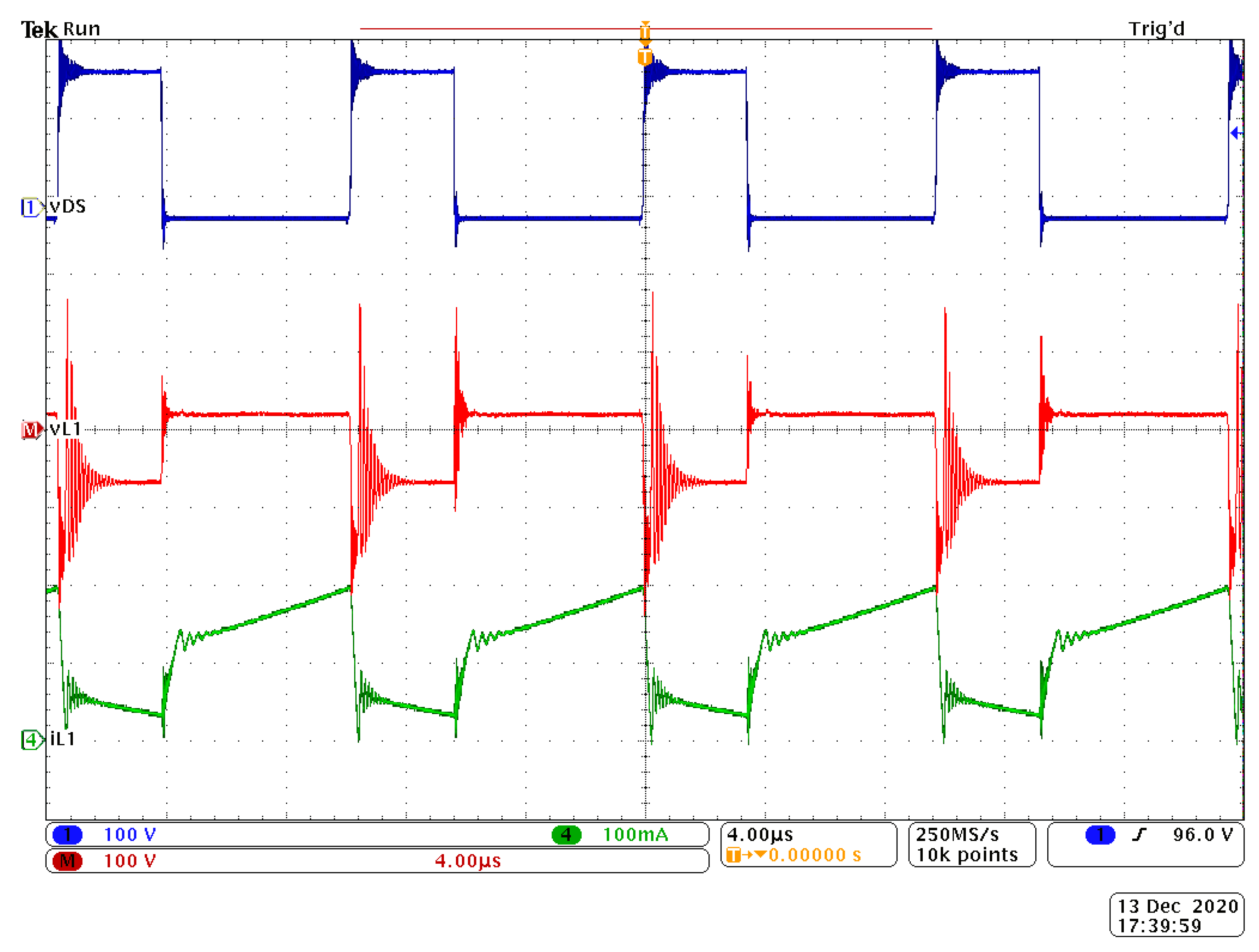
7. Experimental Results

In order to validate the feasibility of the proposed converter, a prototype was built with the same parameters like in the design example. The chosen transistor was Infineon Mosfet STW37N60DM2AG and the chosen diodes D1,2,4 was of RFN10NS6SFH type. In all the acquired waveforms the reference signal on the oscilloscope was the drain-to source voltage of the transistor Q. The experiments were performed, with a fixed input voltage Vg = 35 V, a fixed switching frequency fs = 100 kHz and a load R = 360 Ω.
The acquired waveforms for a duty cycle D = 0.2 are shown in Figure 19. It can be remarked that at this low duty cycle the operation is in DCM with respect to diodes D1 and D2. This is confirmed by Equation (25).
The acquired waveforms for a duty cycle D = 0.66 are shown in Figure 20, Figure 21, Figure 22 and Figure 23. The typical rectangular shape for inductor voltages and triangular shape for the inductor currents with corresponding monotonicity can be remarked, like in the theory. These waveforms also match the simulated ones and the rectangular shape of the inductor voltages and piece-wise linear shape of the inductor currents are verified both regarding monotonicity and phase.
The static conversion ratio for the prototype was measured modifying the duty cycle D and measuring the output voltage, Vo. The comparison between the ideal conversion ratio, theoretical conversion ratio in the presence of the conduction losses and the measured one is presented in Figure 24. It can be remarked that: up to a duty cycle of 0.6, all three curves are almost overlapping. At higher duty cycles the measured curve deviates, which is a typical phenomenon encountered in converters with step-up nature. In Figure 25, the theoretical statical conversion ratio in the presence of losses is presented at very high duty cycles. It can be remarked that the theoretical curve in the presence of conduction losses reaches a maximum and then start to decrease. This is a typical behavior in step-up converters in which the maximum attainable conversion ratio is a finite and limited value. The dependency of the efficiency against the output power at a constant output voltage of 120 V is shown in Figure 26.

8. Conclusions

This paper introduces a new converter that has the conversion ratio (1 + nD) times higher than the classical Ćuk topology. Therefore, in the step-up region, a wide static conversion ratio is achieved, being useful in applications where there is very big difference between the input and output voltage. Compared to the classical Ćuk converter, it includes two additional diodes but it exhibits lower semiconductor dc current stresses. Moreover, the turns ratio brings an additional degree of freedom that facilitate the design process. The operating principle, the steady state equations are revealed, the main waveforms are presented and the relationship for designing the converter are provided. The simulation and the experimental results validate the theoretical consideration, thus confirming the feasibility and the applicability of the proposed converter.

Author Contributions

The authors have equal contribution. Conceptualization, I.-M.P.-C., M.B. and D.L.; software, M.B. and D.L.; simulation, I.-M.P.-C. and M.B.; practical implementation I.-M.P.-C., M.B. and D.L.; validation, I.-M.P.-C. and D.L.; writing—original draft preparation, I.-M.P.-C. and M.B.; writing—review and editing, D.L.; supervision, I.-M.P.-C.; funding acquisition, I.-M.P.-C. All authors have read and agreed to the published version of the manuscript.

Funding

This work was supported by a grant of the Romanian Ministry of Education and Research, CNCS-UEFISCDI, project number PN-III-P1-1.1-PD-2019-1006, within PNCDI III, PD 76/2020.

Conflicts of Interest

The authors declare no conflict of interest.

References

  1. Abdel-Rahim, O.; Orabi, M.; Abdelkarim, E.; Ahmed, M.; Zoussef, M. Switched Inductor Boost Converter for PV Applications. In Proceedings of the 2012 27th Annual IEEE Applied Power Electronics Conference and Exposition (APEC), Orlando, FL, USA, 5–9 February 2012; pp. 2100–2106. [Google Scholar]
  2. Tseng, S.Y.; Wang, H.Y. A photovoltaic power system using a high step-up converter for DC load applications. Energies 2013, 6, 1068–1100. [Google Scholar] [CrossRef] [Green Version]
  3. Pop-Calimanu, I.-M.; Lica, S.; Popescu, S.; Lascu, D.; Lie, I.; Mirsu, R. A New Hybrid Inductor-Based Boost DC-DC Converter Suitable for Applications in Photovoltaic Systems. Energies 2019, 12, 252. [Google Scholar] [CrossRef] [Green Version]
  4. Karmahapatra, A.; Choudhury, T.R.; Nayak, B.; Santra, S.B. Design and Analysis of a Quadratic Boost Derived High Step up Converter for DC Micro-grid Application. In Proceedings of the International Conference on Recent Innovations in Electrical, Electronics & Communication Engineering (ICRIEECE), Bhubaneswar, India, 27–28 July 2018; pp. 3151–3155. [Google Scholar]
  5. Maroti, P.K.; Padmanaban, S.; Bhaskar, M.S.; Blaabjerg, F.; Wheeler, P. New Inverting Modified CUK Converter Configurations with Switched Inductor (MCC) for High-Voltage/Low-Current Renewable Applications. In Proceedings of the 20th European Conference on Power Electronics and Applications (EPE’18 ECCE Europe), Riga, Latvia, 17–21 September 2018; pp. 1–10. [Google Scholar]
  6. Hasanpour, S.; Siwakoti, Y.P.; Mostaan, A.; Blaabjerg, F. New Semiquadratic High Step-Up DC/DC Converter for Renewable Energy Applications. IEEE Trans. Power Electron. 2020, 36, 433–446. [Google Scholar] [CrossRef]
  7. Malik, M.Z.; Chen, H.; Nazir, M.S.; Khan, I.A.; Abdalla, A.N.; Ali, A.; Chen, W. A New Efficient Step-Up Boost Converter with CLD Cell for Electric Vehicle and New Energy Systems. Energies 2020, 13, 1791. [Google Scholar] [CrossRef] [Green Version]
  8. Premkumar, M.; Kumar, C.; Sowmya, R. Analysis and Implementation of High-Performance DC-DC Step-Up Converter for Multilevel Boost Structure. Front. Energy Res. 2019, 7, 149. [Google Scholar] [CrossRef] [Green Version]
  9. Anasudheen, P.; Jayanand, B. Negative to positive voltage conversion cuk converter with high boost capability. In Proceedings of the International Conference on Power, Instrumentation, Control and Computing (PICC), Thrissur, India, 9–11 December 2015; pp. 1–5. [Google Scholar]
  10. Umuhoza, J.; Zhang, Y.; Zhao, S.; Mantooth, H.A. An Adaptive Control Strategy for Power Balance and the Intermittency Mitigation in Battery-PV Energy System at Residential DC Microgrid Level. In Proceedings of the 2017 IEEE Applied Power Electronics Conference and Exposition (APEC), Tampa, FL, USA, 26–30 March 2017; pp. 1341–1345. [Google Scholar]
  11. Basaran, K.; Cetin, N.S.; Borekci, S. Energy management for on-grid and off-grid wind/PV and battery hybrid systems. IET Renew. Power Gener. 2017, 11, 642–649. [Google Scholar] [CrossRef]
  12. Khambuya, R.; Khwan-on, S. A New High Step-down DC-DC Converter for Renewable Energy System Applications. Procedia Comput. Sci. 2016, 86, 349–352. [Google Scholar] [CrossRef] [Green Version]
  13. Cornea, O.; Hulea, D.; Muntean, N.; Andreescu, G.D. Step-Down Switched-Inductor Hybrid DC-DC Converter for Small Power Wind Energy Conversion Systems with Hybrid Storage. IEEE Access 2020, 8, 136092–136107. [Google Scholar] [CrossRef]
  14. Sun, Z.; Bae, S. Multiple-Input Soft-Switching Step-up/down Converter for Renewable Energy Systems. In Proceedings of the 7th International Conference on Renewable Energy Research and Applications (ICRERA), Paris, France, 14–17 October 2018; pp. 632–636. [Google Scholar]
  15. Wu, H.; Sun, K.; Chen, L.; Zhu, L.; Xing, Y. High Step-Up/Step-Down Soft-Switching Bidirectional DC–DC Converter with Coupled-Inductor and Voltage Matching Control for Energy Storage Systems. IEEE Trans. Ind. Electron. 2016, 63, 2892–2903. [Google Scholar] [CrossRef]
  16. Siouane, S.; Jovanović, S.; Poure, P.; Jamshidpour, E. An Efficient Fault Tolerant Cascaded Step-Up Step-Down Converter for Solar PV Modules. In Proceedings of the 2018 IEEE International Conference on Environment and Electrical Engineering and 2018 IEEE Industrial and Commercial Power Systems Europe (EEEIC/I&CPS Europe), Palermo, Italy, 12–15 June 2018; pp. 1–5. [Google Scholar]
  17. Chen, M.M.; Cheng, K.W.E. A new bidirectional DC-DC converter with a high step-up/down conversion ratio for renewable energy applications. In Proceedings of the 2016 International Symposium on Electrical Engineering (ISEE), Hong Kong, China, 16–18 March 2016; pp. 1–6. [Google Scholar]
  18. Moury, S.; Lam, J. New soft-switched high frequency multi-input step-up/down converters for high voltage DC-distributed hybrid renewable systems. In Proceedings of the 2017 IEEE Energy Conversion Congress and Exposition (ECCE), Cincinnati, OH, USA, 1–5 October 2017; pp. 5537–5544. [Google Scholar]
  19. Baliwant, B.B.; Gothane, A.R.; Waghmare, V.B. Hardware Implementation of DC-DC SEPIC Converter for Applications of Renewable Energy Using PWM Based Charge Controller. In Proceedings of the 3rd International Conference on Electronics, Communication and Aerospace Technology (ICECA), Coimbatore, India, 12–14 June 2019; pp. 562–565. [Google Scholar]
  20. Gholizadeh, H.; Sarikhani, A.; Hamzeh, M. A Transformerless Quadratic Buck-Boost Converter Suitable for Renewable Applications. In Proceedings of the 10th International Power Electronics, Drive Systems and Technologies Conference (PEDSTC), Shiraz, Iran, 12–14 February 2019; pp. 470–474. [Google Scholar]
  21. Paul, A.K.; Paul, S.; Paul, B. Transformerless Buck-Boost Converter with Positive Output Voltage and Feedback. Int. J. Eng. Res. Technol. (IJERT) 2017, 6, 656–661. [Google Scholar]
  22. Zhu, M.; Luo, F.L. Enhanced Self-Lift Cûk Converter for Negative-to-Positive Voltage Conversion. IEEE Trans. Power Electron. 2010, 25, 2227–2233. [Google Scholar] [CrossRef]
  23. Galea, F.; Apap, M.; Spiteri Staines, C.; Cilia, J. Design of a high efficiency wide input range isolated Ćuk Dc-Dc converter for grid connected regenerative active loads. In Proceedings of the World Engineers’ Convention, Geneva, Switzerland, 4–9 September 2011. [Google Scholar]
  24. Lica, S.; Pop-Calimanu, I.M.; Lascu, D.; Popescu, S.; Tomoroga, M.; Ciresan, A. A New Hybrid Ćuk Converter. In Proceedings of the International Symposium on Electronics and Telecommunications (ISETC), Timisoara, Romania, 8–9 November 2018; pp. 1–4. [Google Scholar]
  25. Axelrod, B.; Berkovich, Y.; Ioinovici, A. Switched capacitor/switched inductor structures for getting transformerless hybrid dc-dc PWM converters. IEEE Trans. Circuits Syst. I Regul. Pap. 2008, 55, 687–696. [Google Scholar] [CrossRef]
  26. Axelrod, B.; Berkovich, Y.; Ioinovici, A. Hybrid switched-capacitor-Cuk/Zeta/Sepic converters in step-up mode. In Proceedings of the IEEE International Symposium on Circuits and Systems, Kobe, Japan, 23–26 May 2005; Volume 2, pp. 1310–1313. [Google Scholar]
  27. Axelrod, B.; Berkovich, Y.; Ioinovici, A. Switched-capacitor (SC)/switched inductor (SL) structures for getting hybrid step-down Cuk/Sepic/Zeta converters. In Proceedings of the IEEE International Symposium on Circuits and Systems, Island of Kos, Greece, 21–24 May 2006; p. 4. [Google Scholar]
  28. Axelrod, B.; Berkovich, Y.; Tapuchi, S.; Ioinovici, A. Steep conversion ration Ćuk, Zeta, and Sepic converters based on a switched coupled-inductor cell. In Proceedings of the IEEE Power Electronics Specialists Conference, Rhodes, Greece, 15–19 June 2008; pp. 3009–3014. [Google Scholar]
  29. Maksimovic, D.; Ćuk, S. Switching Converters with Wide DC Conversion Range. IEEE Trans. Power Electron. 1991, 6, 151–157. [Google Scholar] [CrossRef]
  30. Erickson, R.W.; Maksimovic, D. Fundamentals of Power Electronics, 2nd ed.; Kluwer Academic Publishers: New York, NY, USA, 2001. [Google Scholar]
  31. Ćuk, S. A new zero-ripple switching DC-to-DC converter and integrated magnetics. IEEE Trans. Magn. 1983, 19, 57–75. [Google Scholar] [CrossRef] [Green Version]
  32. Middlebrook, R.D.; Cuk, S. A general unified approach to modelling switching-converter power stages. In Proceedings of the IEEE Power Electronics Specialists Conference, Cleveland, OH, USA, 8–10 June 1976; pp. 18–34. [Google Scholar]
  33. Anand, A.; Singh, B.; Chandra, A.; Al-Haddad, K. Isolated Cuk Converter with Two Symmetrical Output voltages for SRM Drive. In Proceedings of the IEEE Wireless Power Transfer Conference (WPTC), Montreal, QC, Canada, 3–7 June 2018; pp. 1–4. [Google Scholar]
  34. Li, C.; Herrera, L.; Jia, J.; Fu, L.; Isurin, A.; Cook, A.; Huang, Y.; Wang, J. Design and Implementation of a Bidirectional Isolated Ćuk Converter for Low-Voltage and High-Current Automotive DC Source Applications. IEEE Trans. Veh. Technol. 2014, 63, 2567–2577. [Google Scholar] [CrossRef]
  35. Simulation Research; Caspoc Simulation Program. Available online: http://www.simulationresearch (accessed on 22 October 2020).
Figure 1. The initial Ćuk step-up converter with the switching cell Up3 [25].
Electronics 09 02188 g001
Figure 2. The novel proposed hybrid Ćuk-type dc-dc converter with coupled inductors.
Electronics 09 02188 g002
Figure 3. Equivalent schematic of the proposed hybrid Ćuk dc-dc converter with coupled inductors.
Electronics 09 02188 g003
Figure 4. The equivalent circuits of the proposed hybrid Ćuk dc-dc converter with coupled inductors in CCM: (a) First topological state; (b) Second topological state.
Electronics 09 02188 g004
Figure 5. Main waveforms associated to the magnetizing inductor LM and the inductor L3.
Electronics 09 02188 g005
Figure 6. Main waveforms associated to the internal capacitor C and output capacitor Co.
Electronics 09 02188 g006
Figure 7. Main semiconductor waveforms.
Electronics 09 02188 g007
Figure 8. Static conversion ratio against duty cycle for the proposed converter (for n = 1.3, 2.2 and 3.4) and for the classical Ćuk converter.
Electronics 09 02188 g008
Figure 9. Caspoc Simulation. Output dc voltage.
Electronics 09 02188 g009
Figure 10. Voltage and current corresponding to the primary winding.
Electronics 09 02188 g010
Figure 11. Voltage and current corresponding to the secondary winding.
Electronics 09 02188 g011
Figure 12. Voltage and current corresponding to inductor L3.
Electronics 09 02188 g012
Figure 13. Voltage and current corresponding to internal capacitor C.
Electronics 09 02188 g013
Figure 14. Voltage and current corresponding to output capacitor CO.
Electronics 09 02188 g014
Figure 15. Voltage and current waveform for transistor Q.
Electronics 09 02188 g015
Figure 16. Voltage and current corresponding to diode D1.
Electronics 09 02188 g016
Figure 17. Voltage and current corresponding to diode D2.
Electronics 09 02188 g017
Figure 18. Voltage and current corresponding to diode D4.
Electronics 09 02188 g018
Figure 19. Oscilloscope waveforms: drain-to-source voltage (dark blue-vDS); gate-to-source voltage (purple-vGS); current through L2 at the duty cycle D = 0.2.
Electronics 09 02188 g019
Figure 20. Oscilloscope waveforms: drain-to-source voltage (dark blue-vDS); voltage across the primary (red-vL1); the primary current L1 (green-iL1). Duty cycle D = 0.66.
Electronics 09 02188 g020
Figure 21. Oscilloscope waveforms: drain-to-source voltage (dark blue-vDS); voltage across the secondary L2 (red-vL2); secondary current (green-iL2). Duty cycle D = 0.66.
Electronics 09 02188 g021
Figure 22. Oscilloscope waveforms: drain-to-source voltage (dark blue-vDS); voltage across L3 (red-vL3); output voltage (light blue-VO) and current through L3 (green-iL3). Duty cycle D = 0.66.
Electronics 09 02188 g022
Figure 23. Oscilloscope waveforms: drain-to-source voltage (dark blue-vDS); gate-to-source voltage (purple); output voltage (light blue-VO), current through L3 (green-iL3). Duty cycle D = 0.66.
Electronics 09 02188 g023
Figure 24. The experimental static conversion ratio against the duty cycle (blue) compared to the ideal one (purple) and the theoretical one in the presence of conduction losses (red).
Electronics 09 02188 g024
Figure 25. The theoretical dependency of the static conversion ratio on the duty cycle in the presence of losses considering an extended duty cycle range, revealing the maximum attainable dc gain.
Electronics 09 02188 g025
Figure 26. The experimental efficiency against the output power.
Electronics 09 02188 g026
Table 1. Comparison between main parameters of different step-up converters.
ParameterType of Converter
Classical Buck-Boost [30]Classical Ćuk [32]Hybrid Ćuk [24]Proposed Hybrid Ćuk
Switches1111
Diodes1133
Total no. of components4688
System order2444
Static conversion ratio-M D 1 D D 1 D D · ( n + D ) n · ( 1 D ) D · ( 1 + n · D ) 1 D
Duty cycle-D M 1 + M M 1 + M A n · ( 1 + M ) 2 B ( 1 + M ) 2 n
Switch current stress M 2 · V g R M · ( 1 + M ) · V g R M 2 · V g R M 2 · V g R
Switch voltage stress ( 1 + M ) · V g ( 1 + M ) · V g 2 · M · V g n n · M + A 2 n M · V g 1 M + B
Maximum diode dc current stress M 2 · V g R M · ( 1 + M ) · V g R M · V g R M · V g R
Maximum diode voltage stress ( 1 + M ) · V g ( 1 + M ) · V g 2 · M · V g n n · M + A 2 n M · V g 1 M + B
where, A = n 2 ( 1 + M ) 2 + 4 nM , B = ( 1 + M ) 2 + 4 n M .
Publisher’s Note: MDPI stays neutral with regard to jurisdictional claims in published maps and institutional affiliations.

