Optimization of the Ablative Laser Cutting of Shadow Mask for Organic FET Electrode Fabrication

Abstract
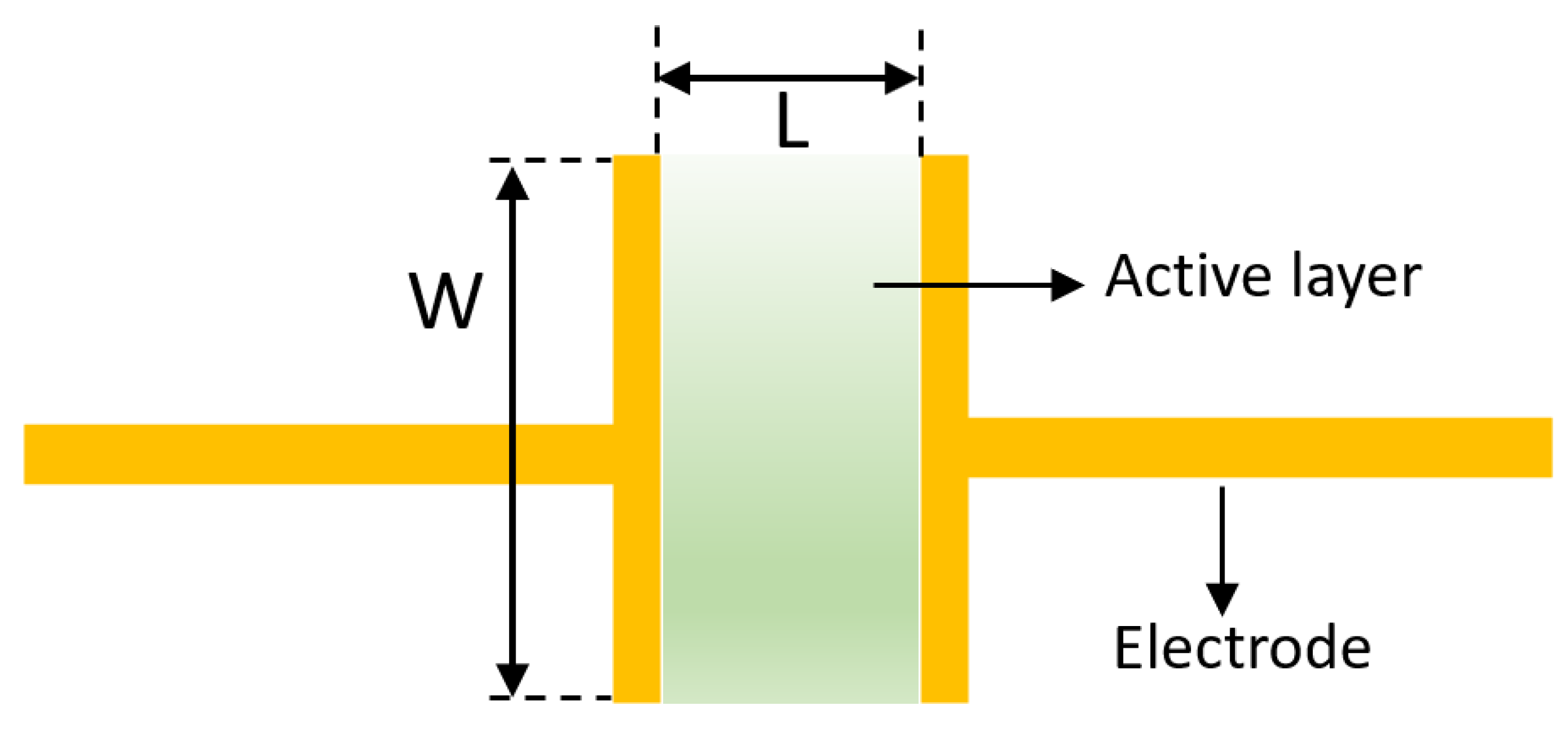
:1. Introduction
2. Materials and Methods
2.1. Laser Process
- Stainless steel SMT stencil foils PhD, 120 µm thick;
- Cold-rolled stainless, spring steel-1.4310, 35 µm thick;
- Hardened steel 1.1274, 30 µm thick.
2.2. Optimalization of the Mask-Cutting Process
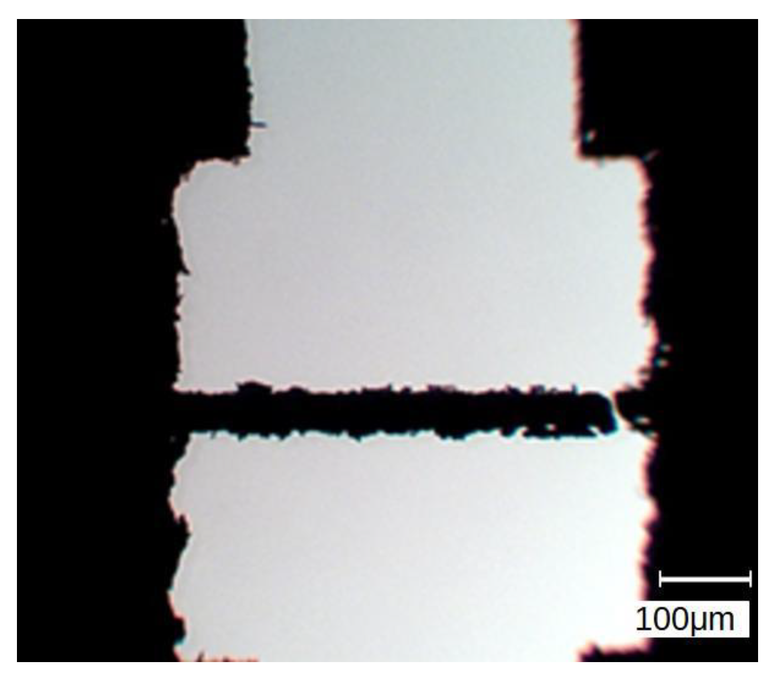
3. Results
4. Discussion
Author Contributions
Funding
Acknowledgments
Conflicts of Interest
References
- Farson, F.; Feeley, D.F.T. (Eds.) LIA Handbook of Laser Materials Processing; Springer: Berlin/Heidelberg, Germany, 2001. [Google Scholar]
- Steen, W.M.; Mazumder, J. Laser Material Processing, 4th ed.; Springer: London, UK; Dordrecht, The Netherlands; Heidelberg, Germany; New York, NY, USA, 2010. [Google Scholar]
- Banat, D.; Ganguly, S.; Meco, S.; Harrison, P. Application of high power pulsed nanosecond fibre lasers in processing ultra-thin aluminium foils. Opt. Lasers Eng. 2020, 129, 106075. [Google Scholar] [CrossRef]
- Korzeniewska, E.; Tomczyk, M.; Pietrzak, Ł.; Hadžiselimović, M.; Štumberger, B.; Sredenšek, K.; Seme, S. Efficiency of laser-shaped photovoltaic cells. Energies 2020, 13, 4747. [Google Scholar] [CrossRef]
- Pawlak, R.; Tomczyk, M.; Walczak, M.; Sek, P.; Tanski, M. The efficiency and quality of silicon micromachining above the ablation threshold: A comparison for femto, pico and nanosecond laser. In Proceedings of the SPIE—The International Society for Optical Engineering, Jastarnia, Poland, 24–28 September 2018; Volume 10974, p. 109740X. [Google Scholar]
- Pawlak, R.; Tomczyk, M.; Walczak, M.; Domagalski, P. Semiconductor and ceramic microstructure made by single mode fiber laser. J. Phys. Conf. Ser. 2014, 494, 012015. [Google Scholar] [CrossRef] [Green Version]
- Siciński, M.; Korzeniewska, E.; Tomczyk, M.; Pawlak, R.; Bieliński, D.; Gozdek, T.; Kaluzinska, K.; Walczak, M. Laser-textured rubbers with carbon nanotube fillers. Polymers 2018, 10, 1091. [Google Scholar]
- Ahmadivand, A.; Gerislioglu, B.; Ramezani, Z. Toroidal Metamaterials: Fundamentals, Devices, and Applications; Springer Nature: Berlin/Heidelberg, Germany, 2020. [Google Scholar]
- Ahmadivand, A.; Gerislioglu, B.; Ahuja, R.; Mishra, A.K. Toroidal metaphotonics and metadevices. Laser Photon. Rev. 2020, 14, 1900326. [Google Scholar] [CrossRef]
- Ahmadivand, A.; Semmlinger, M.; Dong, L.; Gerislioglu, B.; Nordlander, P.; Halas, N.J. Toroidal dipole-enhanced third harmonic generation of deep ultraviolet light using plasmonic meta-atoms. Nano Lett. 2019, 19, 605–611. [Google Scholar]
- Pawlowski, S.; Plewako, J.; Korzeniewska, E. Analysis of flow field distribution in a thin conductive layer with an elliptical defect. Przegląd Elektrotechniczy 2020, 96, 234–237. [Google Scholar]
- Servaites, J.D.; Ratner, M.A.; Marks, T.J. Organic solar cells: A new look at traditional models. Energy Environ. Sci. 2011, 4, 4410–4422. [Google Scholar] [CrossRef]
- Someya, T.; Bauer, S.; Kaltenbrunner, M. Imperceptible organic electronics. MRS Bull. 2017, 42, 124–130. [Google Scholar] [CrossRef]
- Nawrocki, R.A.; Matsuhisa, N.; Yokota, T.; Someya, T. 300-nm Imperceptible, Ultraflexible, and Biocompatible e-Skin Fit with Tactile Sensors and Organic Transistors. Adv. Electron. Mater. 2016, 2, 2–5. [Google Scholar] [CrossRef]
- Bardagot, O.; Kubik, P.; Marszalek, T.; Veyre, P.; Medjahed, A.A.; Sandroni, M.; Grévin, B.; Pouget, S.; Domschke, T.N.; Carella, A.; et al. Impact of Morphology on Charge Carrier Transport and Thermoelectric Properties of N-Type FBDOPV-Based Polymers. Adv. Funct. Mater. 2020, 30, 1–11. [Google Scholar] [CrossRef]
- TSekitani, T.; Zschieschang, U.; Klauk, H.; Someya, T. Flexible organic transistors and circuits with extreme bending stability. Nat. Mater. 2010, 9, 1015–1022. [Google Scholar] [CrossRef] [PubMed]
- Zhang, L.; Wang, H.; Zhao, Y.; Guo, Y.; Hu, W.; Yu, G.; Liu, Y. Substrate-Free Ultra-Flexible Organic Field-Effect Transistors and Five-Stage Ring Oscillators. Adv. Mater. 2013, 25, 5455–5460. [Google Scholar] [CrossRef] [PubMed]
- Ren, H.; Tang, Q.; Tong, Y.; Liu, Y. 320-nm Flexible Solution-Processed 2,7-dioctyl[1] benzothieno[3,2-b]benzothiophene Transistors. Materials 2017, 10, 918. [Google Scholar] [CrossRef] [Green Version]
- Choi, H.H.; Cho, K.; Frisbie, C.D.; Sirringhaus, H.; Podzorov, V. Critical assessment of charge mobility extraction in FETs. Nat. Mater. 2018, 17, 2–7. [Google Scholar] [CrossRef]
- Horowitz, G. Organic thin film transistors: From theory to real devices. J. Mater. Res. 2004, 19, 1946–1962. [Google Scholar] [CrossRef] [Green Version]
- Zhou, Y.X.; Johnson, A.T.; Hone, J.; Smith, W.F. Simple Fabrication of Molecular Circuits by Shadow Mask Evaporation. Nano Lett. 2003, 3, 1371–1374. [Google Scholar] [CrossRef]
- Naulleau, P. Optical Lithography; Elsevier Ltd.: Amsterdam, The Netherlands, 2019; Volume 1–5. [Google Scholar]
- Korzeniewska, E.; Tomczyk, M.; Walczak, M. The influence of laser modification on a composite substrate and the resistance of thin layers created using the PVD process. Sensors 2020, 20, 1920. [Google Scholar] [CrossRef] [Green Version]
- Pramanik, D.; Goswami, S.; Kuar, A.; Sarkar, S.; Mitra, S. A Parametric Study of Kerf Deviation in Fiber Laser Micro Cutting on Ti6Al4V Superalloy. Mater. Today Proc. 2019, 18, 3348–3356. [Google Scholar]
- QLin, Q.; Fan, Z.; Wang, W.; Yan, Z.; Zheng, Q.; Mei, X. The effect of spot overlap ratio on femtosecond laser planarization processing of SiC ceramics. Opt. Laser Technol. 2020, 129, 106270. [Google Scholar]
- Decker, W.; Belan, R.; Heydemann, V.; Armstrong, S.; Fisher, T. Novel low pressure sputtering source and improved vacuum deposition of small patterned features using precision shadow masks. In Proceedings of the Society of Vacuum Coaters 59th Annual Technical Conference, Indianapolis, IN, USA, 9–13 May 2016; Volume 1, pp. 556–571. [Google Scholar] [CrossRef]
- Ablat, A.; Kyndiah, A.; Houin, G.; Alic, T.Y.; Hirsch, L.; Abbas, M. Role of Oxide/Metal Bilayer Electrodes in Solution Processed Organic Field Effect Transistors. Sci. Rep. 2019, 9, 6685. [Google Scholar]
- Lee, J.H.; Kim, S.; Kim, H.; Lee, J. Solvent-dependent performance of solution-processed small-molecule organic field-effect transistors. Org. Electron. 2018, 52, 184–189. [Google Scholar] [CrossRef]


| Laser SPI G3.1 SM 20 W | |
|---|---|
| Wavelength (nm) | 1062 |
| Average power (W) | 20 |
| Pulse duration (ns) | 15–220 |
| Pulse energy (mJ) | ≤0.55 |
| Frequency of repetition (kHz) | 35–290 |
| Quality of beam (M2) | <1.3 |
| Scanner (Nutfield Techn. Inc.) | |
| F-theta lens (mm) | 100–164 |
| Maximum scanning speed (mm/s) | 6000 |
| Pulsed Laser Beam Expander | |
| Mechanical Outline | 7.0 × 8.7 |
Publisher’s Note: MDPI stays neutral with regard to jurisdictional claims in published maps and institutional affiliations. |
© 2020 by the authors. Licensee MDPI, Basel, Switzerland. This article is an open access article distributed under the terms and conditions of the Creative Commons Attribution (CC BY) license (http://creativecommons.org/licenses/by/4.0/).
Share and Cite
Tomczyk, M.; Kubik, P.; Waliszewski, W. Optimization of the Ablative Laser Cutting of Shadow Mask for Organic FET Electrode Fabrication. Electronics 2020, 9, 2184. https://doi.org/10.3390/electronics9122184
Tomczyk M, Kubik P, Waliszewski W. Optimization of the Ablative Laser Cutting of Shadow Mask for Organic FET Electrode Fabrication. Electronics. 2020; 9(12):2184. https://doi.org/10.3390/electronics9122184
Chicago/Turabian StyleTomczyk, Mariusz, Paweł Kubik, and Witold Waliszewski. 2020. "Optimization of the Ablative Laser Cutting of Shadow Mask for Organic FET Electrode Fabrication" Electronics 9, no. 12: 2184. https://doi.org/10.3390/electronics9122184