Article

Analysis of Symmetric Dual Switch Converter under High Switching Frequency Conditions

1
State Key Laboratory of Reliability and Intelligence of Electrical Equipment, Hebei University of Technology, Tianjin 300130, China
2
Laboratory of Electromagnetic Field and Electrical Apparatus Reliability of Hebei Province, Hebei University of Technology, Tianjin 300130, China
*
Author to whom correspondence should be addressed.
Electronics 2020, 9(12), 2183; https://doi.org/10.3390/electronics9122183
Submission received: 12 November 2020 / Revised: 12 December 2020 / Accepted: 15 December 2020 / Published: 18 December 2020
(This article belongs to the Special Issue High-Frequency Power Converters)

Abstract

:
Electric vehicle batteries have the problem of low output voltage, so the application of a high-gain converter is a research hotspot. The symmetrical dual-switch high gain converter has the merits of simple structure, low voltage and current stress, and low EMI. Due to the deterioration of circuit performance caused by circuit parasitic parameters under high frequency operating conditions, the former analysis under low frequency condition cannot satisfy the requirements for performance evaluation. To clarify whether the symmetrical dual-switch high-gain converter can maintain its operating characteristics under high-frequency operating conditions, this paper establishes the converter model considering parasitic parameters, and deduces the sneak circuit modes at high frequency. The effects of parasitic parameters at high frequency on voltage gain, switch stress, and symmetrical operating are analyzed, which is beneficial for the selection and optimization of power devices. This paper believes that considering parasitic parameters may reduce the output gain of the symmetrical double-switch high-gain converter considering parasitic parameters under high frequency conditions, increase the switching stress, and affect the symmetry of the circuit operation when the parasitic parameter values are different. Finally, an experimental platform rated on 200 W with 200 kHz switching frequency is established, and experimental verification is given to verify the analysis.

1. Introduction

With the increasingly serious problems of environmental pollution and energy crisis, the new energy vehicle battery has gradually become a research hotspot in the field of new energy vehicles [1]. The new energy vehicle battery refers to a kind of power source that provides driving power source for electric vehicles, electric trains, electric bicycles, and other transportation tools. Compared with battery usage scenarios such as the energy supply of electronic and electrical equipment and the energy storage of energy storage power stations, the new energy vehicle battery has to adapt to the harsh usage scenarios of various vehicles. This requires that the battery should have the characteristics of high energy density, high charge and discharge power, high safety, long life, and low cost. Currently, there are many different types of battery technology systems that can provide power for vehicles, including lead–acid batteries, nickel–metal hydride batteries, lithium-ion batteries, supercapacitors, metal–air batteries, etc.
The new energy vehicle battery is the core component of the power system of electric vehicles, and its comprehensive performance directly affects the performance of electric vehicles. Electric vehicle power battery packs provide traction for electric vehicles and supply energy to vehicle equipment—such as vehicle air conditioners, lighting equipment, etc. Due to the slow dynamic response of the new energy vehicle battery and the large voltage variation range, high gain DC/DC converter is necessary to achieve the high DC (direct current) bus voltage. Compared to isolated converter, the non-isolated high gain converter has the merits such as low cost, high efficiency, convenient to control, and so on [2]. Most of the non-isolated high-gain converters are derived from Boost converter. Commonly used voltage lifting method includes cascading, switched capacitor, and coupled inductors [3,4,5]. The above-mentioned boost converter has problems such as insufficient gain range, excessive switching stress of the device, and EMI (electromagnetic interference) problems. Compared to the high gain converters, the dual switch converter has the advantages of simple structure, high efficiency, low voltage, and current stress [6], while the asymmetric structure induces the unbalance across the power switches. A symmetric dual switch converter is derived to overcome the above disadvantage, it has the advantages of symmetrical circuit structure, internal voltage clamping, small EMI, etc. The symmetric dual switch converter can realize steady-state and dynamic voltage equalization of switches [7].
The symmetric dual switch converter circuit can reflect the working condition of the circuit based on ideal analysis model at low switching frequency [8]. In order to further improve the power density, a higher switching frequency is required. However, high switching frequency is inflicted with higher switching loss that can considerably reduce the power efficiency of power electronic systems [9]. Therefore, the former analysis under low frequency condition cannot satisfy the requirements for performance evaluation. As a result, many researchers considered parasitic components in their analytical models. Investigations into the effect of parasitic components under high frequency conditions can be summarized as the switching performances of MOSFET (metal-oxide-semiconductor field-effect transistor), switching loss, electromagnetic interference problems, the line current total harmonic distortion of Boost PFC (power factor correction) converter, and the voltage gain of the converter [10,11,12,13,14]. In early research, Gutsmann measured the effects of parasitic components in the power electronic systems by circuit simulations [15]. In Reference [16], the parasitic components were researched individually, the effect of parasitic inductance on MOSFET switching characteristics is studied through experiment. Xiong and Murthy-Bellur have analyzed the impacts of parasitic components and also provided solutions [17]. In Reference [18], the sneak circuit modal analysis method is used to analyze the changes in the operating characteristics of the DCM (discontinuous conduction mode) boost converter after considering the parasitic parameters. After analyzing the effect on gain and stress, the feasibility of the sneak circuit analysis method is proved.
Refer to the analysis content and analysis ideas of the above documents, this paper analyzes the sneak circuit and operating characteristics of the symmetrical dual-switch high gain converter considering parasitic parameters at high frequencies. This paper establishes the converter model considering parasitic parameters, and deduces the sneak circuit modes at high frequency. The effects of parasitic parameters at high frequency on voltage gain, switch stress, and symmetrical operating are analyzed, which is beneficial for the selection and optimization of power devices.
The arrangement of this paper is as follows: in Section 2, the converter model considering devices parasitic parameters at high frequency is established. The sneak modes considering the non-ideal device models are established. In Section 3, the influence of parasitic parameters under high-frequency conditions on the voltage gain, switching stress, and symmetrical operating of the converter is analyzed. The influence of parasitic parameters on the symmetrical performance of the circuit is analyzed. In Section 4, experiments are given to verify the theoretical analysis. Section 5 summarizes the full text of this article.

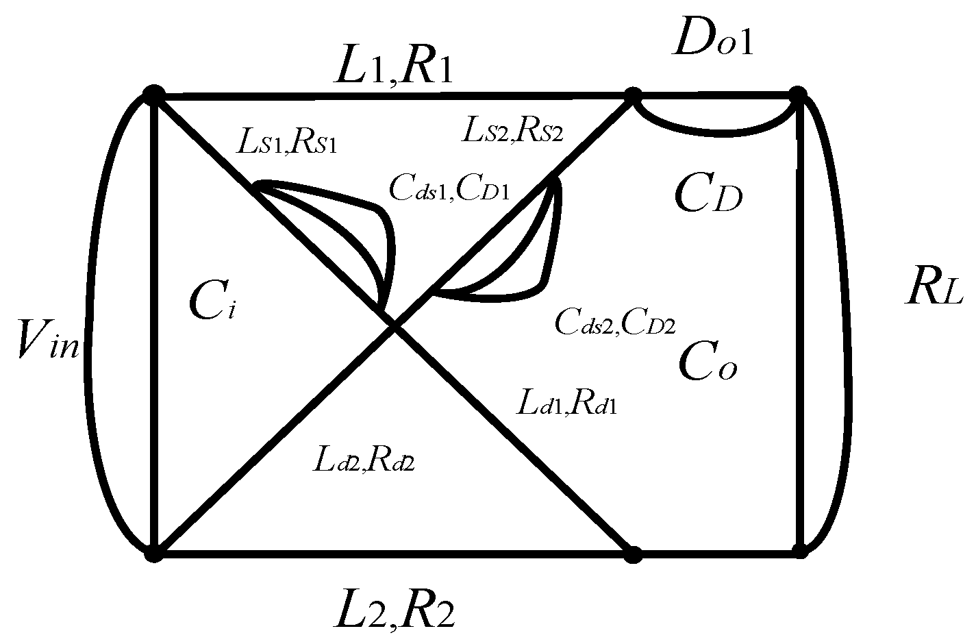
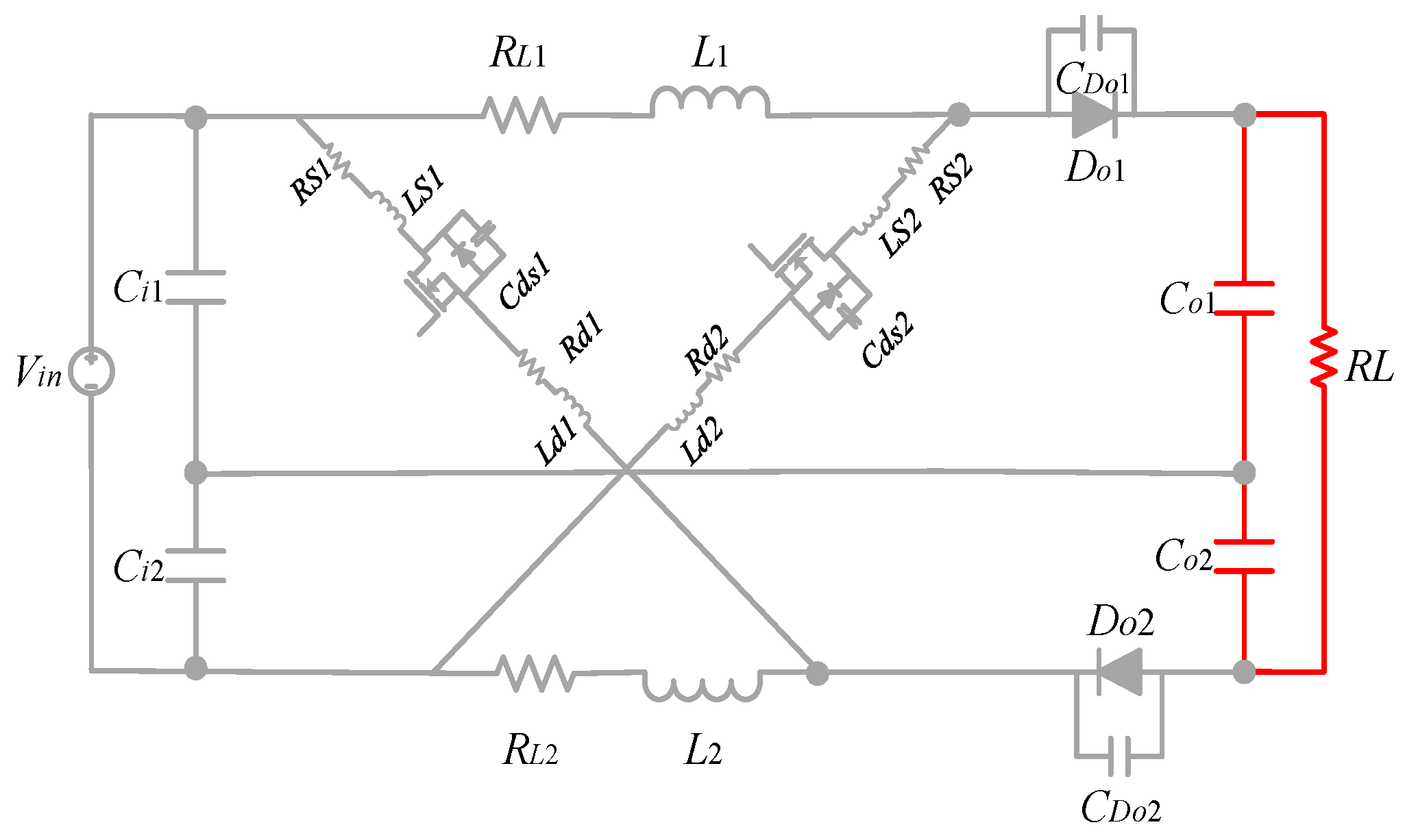
2. Analysis of Sneak Circuit of Dual-Switch Converter with Parasitic Parameters

The circuit topology of the symmetric dual switch high-gain converter is shown in Figure 1. The converter performs parallel charge and series discharge of L1, L2 by controlling the switch to obtain high voltage gain. Since the voltage of the capacitor is constant in steady-state, the voltage of S2 is clamped by Co1 and Ci2, and the voltage of S1 is clamped by Co2 and Ci1. Due to the symmetry of the structure, the converter can achieve the voltage balance of both switches either in steady-state or dynamic-state.
For devices in the converter circuit: the inductors L1, L2 consider its parasitic resistances RL1, RL2; diodes D1, D2 consider their parasitic capacitors CD01, CD02; for MOSFET: Cds1, Cds2 are the parasitic capacitors between the drain-source, Ld_in, Ls_in are the parasitic inductor of the drain and the source. Rs, Rd are the external equivalent parasitic resistor of the switch. Ld_ex, Ls_ex are the external equivalent parasitic inductors of the switch. For the convenience of calculations, let Ld = Ld_in + Ld_ex, Ls = Ls_in + Ls_ex. The converter model after considering parasitic parameters is given in Figure 2.
Use the mesh combination analysis method to analyze the sneak circuit caused by the parasitic parameters at high frequency. First, establish its undirected graph model as shown in Figure 3 below.
According to the mesh combination analysis method, the maximum number of sub-circuits of the dual-switch converter can be obtained as 236. After removing duplicate sub-circuits, 106 actual sub-circuits are obtained. According to the working principle of the converter, the five effective working modes of the converter are obtained. Comparing these five working modes with the ideal working mode, the three normal modes and two sneak circuit modes caused by parasitic parameters under high-frequency conditions are obtained as follows:
For the convenience of reference, the parameters used in this article are defined as follows: URs is the terminal voltage of Rs; URd is the terminal voltage of Rd; ULs is the terminal voltage of Ls; ULd is the terminal voltage of Ld; UCds is the terminal voltage of Cds, UCdsmax is the maximum value of UCds, UCdsmin is the minimum value of UCds, UCdsp-p is the peak-to-peak voltage; IR is the current of Rs; IRd is the current of Rd; ILs is the current of Ls; ILd is the current of Ld; ICds is the current of Cds.

2.1. Analysis of Normal Modes

Mode 1, t [ m T s , t o n ] : When the gate drive voltage reaches UG, the switches are turned on. During this period, the switches S1, S2 remain on, and the diodes D1, D2 remain off. The power supply Vin charges the inductors L1, L2, and the inductor current iL increases linearly. The load side is powered by Co1, Co2. Its equivalent circuit is shown in Figure 4.
Mode 2, t [ t r , t o f f ] : At the time tr, the diodes D1, D2 are still in the conducting state, the energy storage in the power supply and the inductors L1, L2 continues to be transferred to the load, and the inductor current iL decreases linearly. At the same time, all the energy stored in the parasitic inductors Ld, Ls of the MOSFET is released. The equivalent circuit is given in Figure 5.
Mode 3, t [ t D C M , ( m + 1 ) T s ] : Due to the energy consumption of the resistances in the circuit and the parasitic parameters, the inductor current iL will attenuate to zero at time tDCM. At this time, the inductor current can be regarded as zero, and the output capacitors Co1, Co2 continue to provide energy to the load, and their equivalent circuits are shown in Figure 6.

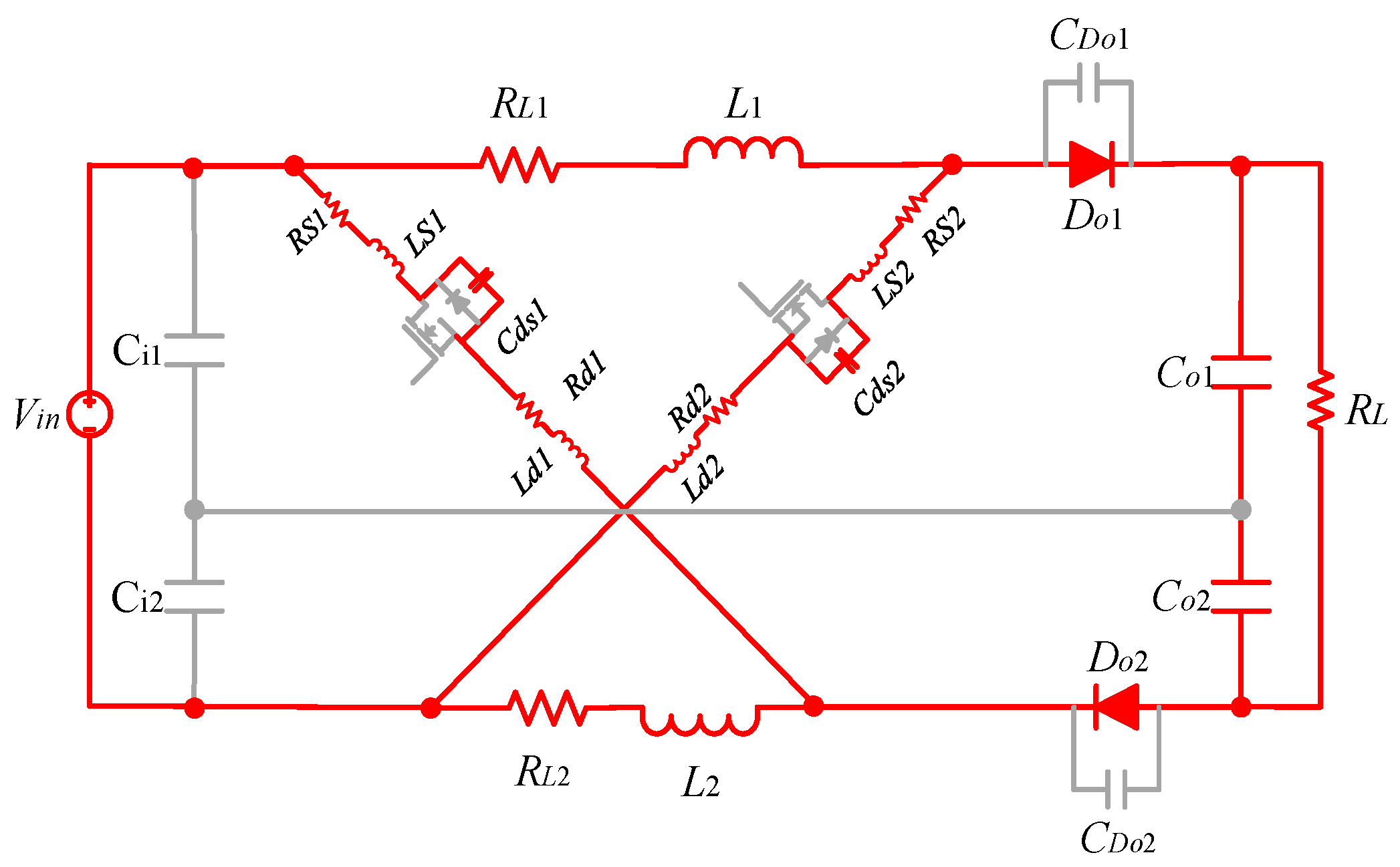
2.2. Analysis of Sneak Modes

Sneak Mode 1, t [ t o n , t r ] : The switches S1, S2 are turned off at the time ton, and the inductor current iL is transferred from the switches S1, S2 to the diodes D1, D2, and the energy is transferred to the load end. At the ton moment, the voltage across CD01 increases from UCDmin to UCdsmax, the voltages across Cds1, Cds2 increase from UCdsmin to UCdsmax. The inductors and the parasitic capacitors in the circuit resonate. The equivalent circuit is shown in Figure 7, and the equations of Sneak Mode 1 can be obtained as
{ i L 1 II = I L 1 ( t o n ) e R L 1 + R L 2 + R e 2 L 1 ( t t o n ) + U i U o U C D max R L 1 + R L 2 + R e 2 [ 1 e R L 1 + R L 2 + R e 2 L 1 ( t t o n ) ] i L 2 II = I L 2 ( t o n ) e R L 1 + R L 2 + R e 1 L 2 ( t t o n ) + U i U o U C D max R L 1 + R L 2 + R e 1 [ 1 e R L 1 + R L 2 + R e 1 L 2 ( t t o n ) ] U C d s p p 1 = 2 U C d s 1 max + U C D max U o ω 1 2 L e 1 C e 1 U C d s p p 2 = 2 U C d s 2 max + U C D max U o ω 2 2 L e 2 C e 2 U C d s max = U o + U i + U C D max 2 i L II R s L d i L II d t U C d s min = U o + U i + U C D min 2 i L II R s L d i L II d t
{ C e 1 = C d s 1 + C g s 1 C g d 1 C g s 1 + C g d 1 , C e 2 = C d s 2 + C g s 2 C g d 2 C g s 2 + C g d 2 ω 1 = 2 1 / L e 1 C e 1 C o C e 1 + C o , ω 2 = 2 1 / L e 2 C e 2 C o C e 2 + C o
It can be seen from the formulas that UCds p-p is very small compared with UCds max. If UCds p-p is small enough at time t > ton, it can be considered that the operation process of the converter circuit at high frequency will cross the Sneak Mode. Set the boundary value equation as U C d s p _ p / U C d s max = ζ . When U C d s p _ p / U C d s max = ζ , the converter can skip Sneak Mode 1 operation.
Sneak Mode 2, t [ t o f f , t D C M ] : When the toff time is reached, the inductor current decreases and then increases in the reverse direction, the parasitic capacitor and the inductor resonate, the voltage across the diode’s parasitic capacitor CD discharges from UCDmax to UCDmin, and the voltage of the switch parasitic capacitor Cds discharges from UCdsmax to UCdsmin. When the discharge voltage reaches the turn-on voltage of diodes, the diodes are turned on, and the converter then enters the reverse recovery process. The equivalent circuit is shown in Figure 8. Similarly, the equations of Sneak Mode 2 can be obtained as
{ i L 1 IV = U i U o U C D maxx ω 1 ( L 1 + L 2 + L e 2 + L q 1 ) e ρ 1 ( t t o f f ) sin ω 1 ( t t o f f ) i L 2 IV = U i U o U C D maxx ω 2 ( L 1 + L 2 + L e 1 + L q 2 ) e ρ 2 ( t t o f f ) sin ω 2 ( t t o f f ) U C D 01 = U i U o ( U i U o U C D max ) e ρ 1 ( t t o f f ) [ cos ω 1 ( t t o f f ) + ρ 1 ω 1 sin ω 1 ( t t o f f ) ]
{ ρ 1 = 2 R L 1 + R e 1 2 L 1 , ρ 2 = 2 R L 2 + R e 2 2 L 2 ω 1 = 1 L 1 ( C D + C e 1 ) ρ 1 2 , ω 2 = 1 L 2 ( C D + C e 2 ) ρ 2 2 C r 1 = C D + C e 1 , C r 2 = C D + C e 2 L q 1 = L e 1 C e 1 C D R o 2 [ C D 2 ( C e 1 + C o ) + C o 2 C r 1 ] ( C r 1 ω 1 2 L e 1 C e 1 C D ) 2 + ω 1 2 R o 2 ( C e 1 C D + C o C r 1 ω 1 2 L e 1 C e 1 C D ) 2 L q 2 = L e 2 C e 2 C D R o 2 [ C D 2 ( C e 2 + C o ) + C o 2 C r 2 ] ( C r 2 ω 2 2 L e 2 C e 2 C D ) 2 + ω 2 2 R o 2 ( C e 2 C D + C o C r 2 ω 2 2 L e 2 C e 2 C D ) 2
The analysis shows that the inductor current iL in Sneak Mode 2 is a sinusoidal wave with resonant angular frequency ω. Substituting the voltage of CD into the previous equation, the voltage expression of UCD can be obtained as
{ U C D min 1 = U i U o + ( U i U o U C D max ) e ρ 1 π ω 1 U C D min 2 = U i U o + ( U i U o U C D max ) e ρ 2 π ω 2 U C D max 1 = ( U i U o ) ( 1 + e ρ 1 π ω 1 ) + 2 U o C e 1 C e 1 + C D U C D max 2 = ( U i U o ) ( 1 + e ρ 2 π ω 2 ) + 2 U o C e 2 C e 2 + C D
From the above analysis of the sneak circuit, considering the parasitic parameters of the devices under high-frequency conditions will cause the converter to resonate due to the parasitic junction capacitors and the inductors in the circuit, which will affect the output characteristic of the converter.
In the DCM mode, the circuit modes operation sequences are Mode 1, Sneak Mode 1, Mode 2, Sneak Mode 2, Mode 3. In the CCM (continuous conduction mode) mode, the circuit modes operation sequences are Mode 1, Sneak Mode 1, Mode 2, Sneak Mode 2. The operation process of the circuit in the CCM mode and the DCM mode is shown in the Figure 9 below.

3. Considering the Influences of Parasitic Parameters on Converter Characteristic

According to the law of conservation of energy, write the following equation for the column
{ U i m T s ( m + 1 ) T s i L d t = U o 2 R L T s + m T s ( m + 1 ) T s ( U R L 1 + U R L 2 ) i L d t U o m T s ( m + 1 ) T s i 0 d t = U o 2 R L T s
During t [ t o n , t o f f ] the inductor current satisfies the equation as
t o n t o f f i L d t = 1 2 D T s I L ( t o n ) = U o R L T s 2 C D ( U C D max U C D min )
Among them, D T s = t o f f t o n .

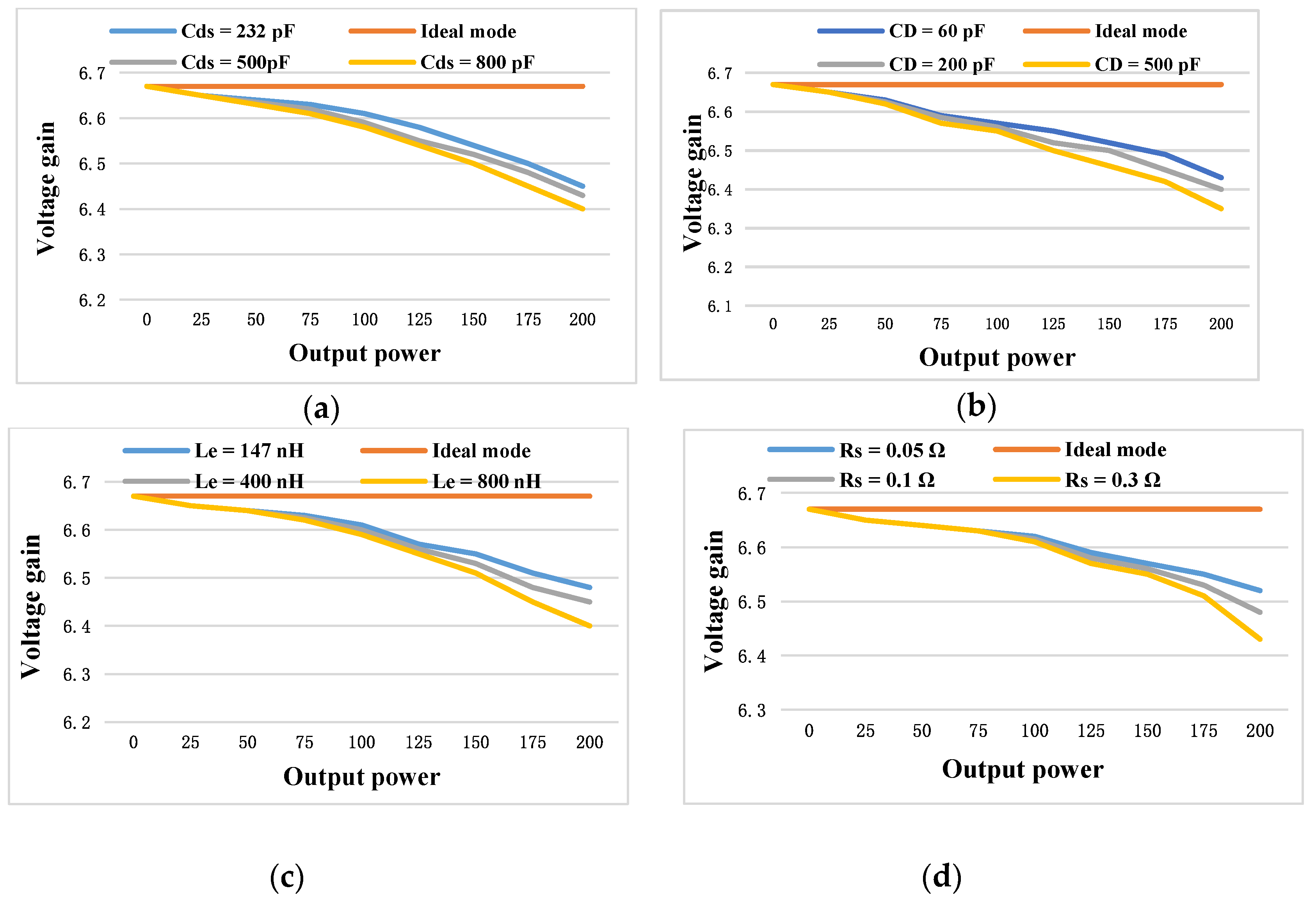
3.1. Effects of Parasitic Parameters on Voltage Gain

  • In the Ideal Case
According to the volt-second equilibrium principle and the relationship between iL and iD in ideal mode, the voltage gain of an ideal dual-switch step-up converter can be obtained as
M = U o U i = 1 + D 1 D
2.
Considering Parasitic Parameters
According to the volt-second equilibrium principle and the law of energy conservation, the voltage gain of the dual-switch converter with parasitic parameters can be obtained as follows:
Switch on period:
U L 1 = U L 2 = U i U R 1 U R e 2
Switch off period:
U L 1 = U L 2 = 1 2 ( U i U o U R L 1 U R L 2 )
Simultaneous equations are obtained:
M = 1 + D [ ( R S + R d + R L ) 2 U i R o + f s C D ( U C D min U C D max ) + f s L e ] 1 e 2 ρ D / f s R S + R d + R L 1 D
From the above equations, the relationship between input voltage and output voltage is a constant value when the circuit parameters and operating period of the converter are determined in the ideal working state. When the converter considering parasitic parameters, the relationship is an exponentially decreasing expression.
Set the rated parasitic parameters values as follows: Cds = 232 pF, CD = 60 pF, Rs = 0.05 Ω, Le = 147 nH. In the case where the ideal circuit parameter values are unchanged, the influences of the changes in the values of each parasitic parameter on the output gain characteristics of the converter are shown in Figure 10.
The above figures show the results that those four parasitic parameters share the common characteristic: the larger the values of the parasitic parameter, the more obvious the effects of reducing the output gain.

3.2. Effects of Parasitic Parameters on Switch Stress

List the voltage and current stress of the switching devices in the ideal model and the model considering parasitic parameters as follows:
  • Ideal conditions
    { I S ¯ = U i L 1 + L 2 D T s U S = M U i 2 I D ¯ = U i L 1 + L 2 D T s U D = M U i
  • Conditions considering parasitic parameters
    { I S 1 ¯ = U i U C d s 1 min R S 1 + R L 1 + R d 1 ( 1 e R S 1 + R L 1 + R d 1 L 1 t ) I S 2 ¯ = U i U C d s 2 min R S 2 + R L 2 + R d 2 ( 1 e R S 2 + R L 2 + R d 2 L 2 t ) U S 1 = U o + U i + U C D max 2 i L II R s L d i L II d t + U C d s 1 max + U C D max U o ω 1 2 L e 1 C e 1 U S 2 = U o + U i + U C D max 2 i L II R s L d i L II d t + U C d s 2 max + U C D max U o ω 2 2 L e 2 C e 2 I D ¯ = U i U C d s min R S 1 + R L 1 + R d 1 ( 1 e R S 1 + R L 1 + R d 1 L 1 t ) U D = U C D min
Set the rated parasitic parameter values as follows: Cds = 232 pF, CD = 60 pF, Rs = 0.05 Ω, Le = 147 nH. The voltage stress of the ideal model and the model considering the parasitic parameter are shown in Figure 11 below.
It can be seen from the above figures that, compared with the voltage stress under ideal conditions, the voltage stress when considering parasitic parameters of the converter is greater. The larger the values of the parasitic capacitors, the larger the amplitude of the resonance voltage of the switches. If the device selection does not consider the impacts of the inductor current fluctuations and the switching stress differences, it may cause new modes or circuit failures in the circuit, which means the selections of devices in circuits under high-frequency conditions must take the effects of parasitic parameters into account.

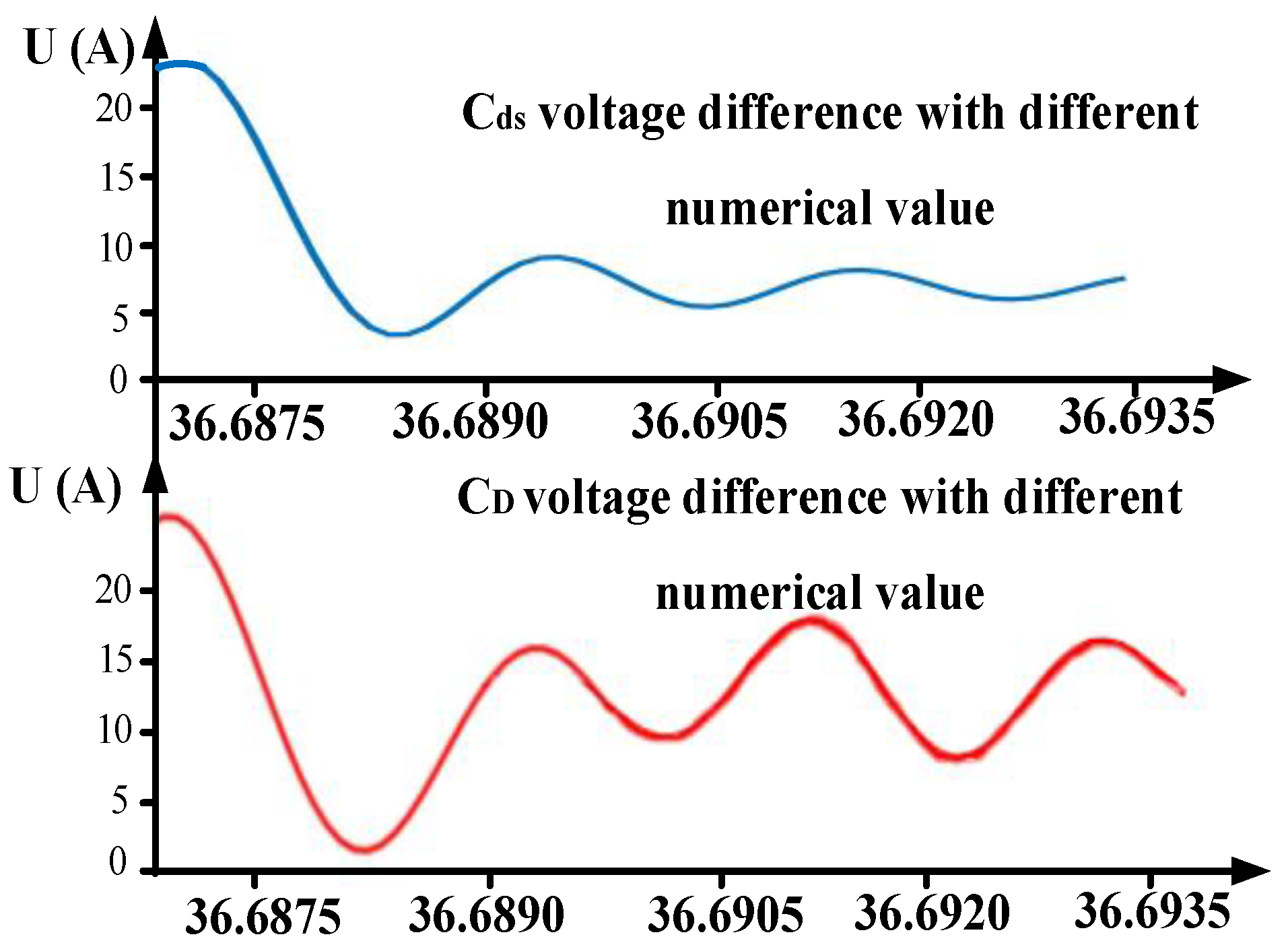
3.3. Influence of Parasitic Parameters Asymmetry on Circuit

In the ideal model, due to the symmetrical structure of the converter, the voltage balance of the switches S1, S2 can be achieved under both steady-state and dynamic conditions, and the centerline has no charge and discharge current. However, if the parasitic parameter values are different for the same type of devices, the symmetric circuit will present an asymmetric working state, which will bring adverse effects on the performance of the converter.
The analysis equations about the voltages of the MOSFET in the sneak modes is re-wrote in this paper to get the expressions of the voltage difference of the parasitic capacitors of the MOSFETs as follows:
Δ U C d s = U C D 01 max U C D 02 max 2 i L II ( R s 1 R s 2 ) ( L 1 L 2 ) d i L II d t
The analytical equations for the inductor current and diode voltage in Sneak Mode is re-wrote in this paper to get the difference expressions as follows:
{ i L 1 IV = U i U o U C D 01 max U C D 02 max ω r 1 ( 2 L 1 + L e 2 + L q ) e ρ 1 ( t t o f f ) sin ω r 1 ( t t o f f ) i L 1 IV = U i U o U C D 01 max U C D 02 max ω r 2 ( 2 L 2 + L e 1 + L q ) e ρ 2 ( t t o f f ) sin ω r 2 ( t t o f f ) U C d s 01 = U i U C d s 1 min R S 1 + R L 2 + R d 1 ( 1 e R S 1 + R L 2 + R d 1 L 1 t ) ρ 1 ω r 1 sin ω r 1 ( t t o f f ) U C d s 02 = U i U C d s 2 min R S 2 + R L 1 + R d 2 ( 1 e R S 2 + R L 1 + R d 2 L 2 t ) ρ 2 ω r 2 sin ω r 2 ( t t o f f ) U C D 01 = ( U i U o U C D 01 max U C D 02 max ) e ρ 1 ( t t o f f ) [ cos ω r 1 ( t t o f f ) + ρ 1 ω r 1 sin ω r 1 ( t t o f f ) ] U C D 02 = ( U i U o U C D 01 max U C D 02 max ) e ρ 2 ( t t o f f ) [ cos ω r 2 ( t t o f f ) + ρ 2 ω r 2 sin ω r 2 ( t t o f f ) ] ρ 1 = 2 R L 1 + R e 1 2 L 1 , ρ 2 = 2 R L 2 + R e 2 2 L 2 ω r 1 = 1 L 1 ( 2 C D + C e 1 ) ρ 1 2 ω r 2 = 1 L 2 ( 2 C D + C e 2 ) ρ 2 2
The influences of the parasitic parameters Cds, CD are reflected in the influences on the oscillation frequency ωr and equivalent inductor Lq. The influences of the parasitic parameter RL are reflected in the influences on oscillation frequency ωr, equivalent parameter ρ, and equivalent inductor Lq. The change of parasitic parameters will result in different inductor current values of iL1, iL2, and the occurrence times of the resonance currents, which makes the charge and discharge currents appear in the centerline of the circuit. The two MOSFETs and diodes have different resonance amplitudes and resonance appearance times. The operation symmetry of the circuit is destroyed, which may cause new modalities or circuit failures. Draw the waveform of the stress difference formulas considering the parasitic parameters as shown in Figure 12.

4. Simulations and Experiment Verification

An experimental platform for the symmetric dual switch high-gain converter is built in the laboratory. The devices selections and parameter values settings of the experimental platform are shown in Table 1.

4.1. Simulations in Saber

The simulated waveforms of the inductor current, switch voltage and diode voltage are shown in Figure 13. The inductor current waveform shows a trend of first rising and then falling. The inductor current, MOSFET voltage, and diode voltage waveforms are all resonant. Compared with ideal conditions, the voltage amplitudes of MOSFETs and diodes are increased due to the influences of resonance when considering parasitic parameters under high-frequency conditions.
The simulation waveforms show that, due to the high-frequency resonance under high-frequency conditions, the amplitudes of inductor currents, MOSFET voltage and diode voltage all increases due to the parasitic capacitors resonate with the inductors in the sneak circuit, in line with the previous analysis.

4.2. Experimental Verification

The experimental platform of the dual-switch high-gain converter built in the laboratory is shown in the Figure 14 below.
The parasitic parameter values of the devices are sot as RS1 = RS2 = 0.05 Ω, Cds1 = Cds2 = 232 pF, in the case of symmetrical parasitic parameters, the experimental waveforms of Po = 200 W are shown in Figure 15.
After the output power in the original experiment is adjusted from 200 W to 80 W, the diagrams of the experimental waveforms of Po = 80 W are shown in Figure 16. From the diagrams of the experimental waveforms, the amplitude of the current resonance reduces 0.4 A, and the amplitude of the MOSFET voltage reduces 8.5 V, which confirms the theoretical analysis.
To verify the effects of different parasitic parameter values of the same type of devices on the converter under high-frequency conditions, the value of the parasitic resistance RL2 is adjusted from 0.05 Ω to 0.1 Ω. The experimental waveforms of Po = 200 W are shown in Figure 17 below.

4.3. Comparative Analysis of Simulation and Experimental Waveforms

The resonance current amplitudes values in experimental waveforms Figure 15a are iL1 = 8.8 A, iL2 = 8.7 A, and resonance current amplitudes values in simulation waveforms Figure 13a are iL1 = 8.9 A, iL2 = 8.7 A. The amplitudes are almost the same.
By comparing the experimental waveforms, the simulation waveforms, and theoretical analysis of the inductor currents, it can be known that the analysis of the influences of the parasitic parameters on the inductor currents is in line with the actual working situations.
The resonance voltage amplitudes values in experimental waveforms Figure 15b are UCds1 = 188 V, UCds2 = 183 V, and voltage amplitudes values in simulation waveforms Figure 13b are UCds1 = 187 V, UCds2 = 184 V. The experimental waveforms of MOSFETs resonant voltages are consistent with the simulated waveforms.
From above analysis, it can be known that the parasitic capacitors and the inductors in the circuit resonate under high-frequency conditions, and the amplitudes of the voltages are increased by the influences of resonance, which is consistent with the conclusions obtained from theoretical analysis.
From the above experimental waveform Figure 17a, it can be seen that the resonance current peak value of the inductor current iL2 is enhanced by 0.64 A compared to iL1, and the appearance time is advanced by 8.3 us. Since the inductor currents iL1 and iL2 no longer maintain the same phase and amplitude, the centerline will have charge and discharge currents. Experimental waveform Figure 17b shows the current in the converter centerline to prove this conclusion. Through the above analysis of the experimental waveforms of the inductor currents iL1 and iL2 in the asymmetric condition, it can be known that the symmetry of the ideal symmetric dual switch high-gain converter will be destroyed and the dynamic balance characteristics of converters will be affected when considering parasitic parameters under high-frequency conditions.
From the experimental waveform Figure 17c, it can be seen that the peak value of the resonance voltage UCds2 increases by 7 V than UCds1, and the phases of the two voltages UCds1, UCds2 are no longer the same. From the waveform Figure 17d, it can be seen that the peak value of the resonance voltage UCD02 increases by 13 V than UCD01, and the phases of the two voltages UCD01, UCD02 are different. Through the above analysis, it can be known that the amplitudes of the resonance voltages of MOSFETs and diodes no longer maintains the same values after considering the parasitic parameters values asymmetry, which puts more precise requirements for the selection of devices and the selection of device-rated voltages in actual applications.
From the above experimental waveforms, it can be seen when the values of the parasitic parameters become larger, the voltage stress values of the corresponding switches will be greater. Through the comparisons of experimental waveforms with the same and different parasitic parameter values, it can be seen that when the parasitic parameter values of the devices are different, the symmetry of the ideal symmetric dual switch high-gain converter will be destroyed and the dynamic balance characteristics of converters will be affected and the resonance voltages amplitudes of the MOSFETs are no longer the same, which puts more precise requirements for the selections of devices and the selections of device rated voltages in actual high-frequency application conditions.
A comparison of voltage gains obtained from the experiment and calculation is shown in Figure 18.
In Condition 1, the values of parasitic parameters are: Cds = 232 pF, CD = 60 pF, Rs = 0.05 Ω, Le = 147 nH. In Condition 2, the values of parasitic parameters are: Cds = 232 pF, CD = 120 pF, Rs = 0.1 Ω, Le = 147 nH. The different values in Figure 18 are acquired by adding external capacitors, inductors, and resistors across the device terminals. Figure 18 proves that by varying the values of parasitic parameters while other parameters remain unchanged, the greater the parasitic parameter values, the more obvious the impacts on the output gain, which consistent with theoretical results. The results of the theoretical analysis and experiments verify that the sneak circuit phenomena can be reduced by choosing the value of parameters appropriately, which means higher requirements for the selection and optimization of power devices.

5. Conclusions

This paper takes the symmetrical dual-tube high-gain converter as the research object, and analyzes the characteristics of the high-frequency down-converter considering the parasitic parameters. A model of the symmetrical dual-switch high-gain converter considering parasitic parameters is established, and two sneak operating modes—Sneak Mode 1 and Sneak Mode 2—are found through sneak circuit analysis. Through the analysis of operating characteristics, it is found that considering the parasitic parameters of devices such as Cds, CD, RL, LS, Ld, and RS under high frequency will reduce the voltage gain, increase the switching stress, and affect the symmetry of the circuit operation when the parasitic parameter values are different. Finally, the conclusions obtained through simulation and experiment are consistent with the theoretical analysis, which proves the correctness of the above analysis. The analysis of the working characteristics of the converter under high frequency in this paper has certain reference value for the selection of devices and the selection of margin under high frequency.

Author Contributions

Methodology, H.T.; software, H.T.; validation, D.K.; formal analysis, H.T.; investigation, Y.T.; resources, H.T.; data curation, D.K.; writing—original draft preparation, D.K.; writing—review and editing, D.K.; visualization, H.T.; supervision, H.T. All authors have read and agreed to the published version of the manuscript.

Funding

This work was funded by the National Natural Science Foundation of China under Grant 51677084, The Hebei Province Science Fund for Distinguished Young Scholars grant number E2020202140, and in part by Support Program (III) for 100 Outstanding Innovative Talents in Universities of Hebei Province under Grant SLRC2019025.

Conflicts of Interest

The authors declare no conflict of interest.

References

  1. Han, J.; Gu, X.; Yang, Y.; Tang, T. Dynamic Improvement with a Feedforward Control Strategy of Bidirectional DC-DC Converter for Battery Charging and Discharging. Electronics 2020, 9, 1738. [Google Scholar] [CrossRef]
  2. Zhang, B.; Qiu, D. Sneak circuits in power converters: Concept, principle and application in CPSS Transactions on Power Electronics and Applications. CPSS Trans. Power Electron. Appl. 2017, 2, 68–75. [Google Scholar] [CrossRef]
  3. Hongchen, L.; Li, F. Novel High Step-Up DC-DC Converter with Active Coupled-Inductor Network for a Sustainable Energy System. IEEE Trans. Power Electron. 2015, 30, 6476–6482. [Google Scholar]
  4. Liu, G.; Zhao, P.; Zhao, M.; Yang, Z.; Chen, H. Electromagnetic Disturbed Mechanism of Electronic Current Transformer Acquisition Card under High Frequency Electromagnetic Interference. Electronics 2020, 9, 1293. [Google Scholar] [CrossRef]
  5. Li, M.; Zhang, B.; Qiu, D. Sneak circuit analysis of Boost converter considering parasitic parameters. In Proceedings of the Applied Power Electronics Conference & Exposition, IEEE, Fort Worth, TX, USA, 16–20 March 2014. [Google Scholar]
  6. Tang, Y.; Wang, T.; He, Y.; Fu, D. Study of a high step-up voltage gain DC/DC converter with passive lossless clamp circuit. In Proceedings of the IEEE IECON, Vienna, Austria, 10–13 November 2013; pp. 1308–1313. [Google Scholar]
  7. Shen, C.-L.; Chen, L.-Z.; Chen, H.-Y. Dual-Input Isolated DC-DC Converter with Ultra-High Step-Up Ability Based on Sheppard Taylor Circuit. Electronics 2019, 8, 1125. [Google Scholar] [CrossRef] [Green Version]
  8. Zhao, B.; Song, Q.; Li, J.; Liu, W.; Liu, G.; Zhao, Y. High-Frequency-Link DC Transformer Based on Switched Capacitor for Medium-Voltage DC Power Distribution Application. IEEE Trans. Power Electron. 2016, 31, 4766–4777. [Google Scholar] [CrossRef]
  9. Zhang, B.; Qiu, D.Y. Sneak Circuits of Power Electronic Converters; Wiley: New York, NY, USA, 2015. [Google Scholar]
  10. Zhaksylyk, Y.; Halvorsen, E.; Hanke, U.; Azadmehr, M. Analysis of Fundamental Differences between Capacitive and Inductive Impedance Matching for Inductive Wireless Power Transfer. Electronics 2020, 9, 476. [Google Scholar] [CrossRef] [Green Version]
  11. Rogina, M.R.; Rodríguez, A.; Vázquez, A.; Lamar, D.G.; Hernando, M.M. Event-Focused Digital Control to Keep High Efficiency in a Wide Power Range in a SiC-Based Synchronous DC/DC Boost Converter. Electronics 2020, 9, 2154. [Google Scholar] [CrossRef]
  12. Ansari, S.A.; Moghani, J.S. A Novel High Voltage Gain Noncoupled Inductor SEPIC Converter. IEEE Trans. Ind. Electron. 2018, 66, 7099–7108. [Google Scholar] [CrossRef]
  13. Ragab, K.; Kozak, M.; Sun, N. Thermal Noise Analysis of a Programmable-Gain Switched-Capacitor Amplifier with Input Offset Cancellation. IEEE Trans. Circuits Syst. II Express Briefs 2013, 60, 147–151. [Google Scholar] [CrossRef]
  14. Muhammad, M.; Armstrong, M.; Elgendy, M.A. A Nonisolated Interleaved Boost Converter for High-Voltage Gain Applications. IEEE J. Emerg. Sel. Top. Power Electron. 2016, 4, 352–362. [Google Scholar] [CrossRef] [Green Version]
  15. Gutsmann, B.; Mourick, P.; Silber, D. Exact inductive parasitic extraction for analysis of IGBT parallel switching including DCB-backside eddy currents. In Proceedings of the 2000 IEEE 31st Annual Power Electronics Specialists Conference, Galway, Ireland, 23 June 2000. [Google Scholar]
  16. Chen, Z.; Boroyevich, D.; Burgos, R. Experimental parametric study of the parasitic inductance influence on MOSFET switching characteristics. In Proceedings of the 2010 International Power Electronics Conference-ECCE ASIA, Sapporo, Japan, 21–24 June 2010. [Google Scholar]
  17. Xiong, F.; Zhang, J.M.; Qian, Z.M. Effect of parasitic parameters on current distortion of boost PFC circuit. Proc. CSEE 2010, 30, 40–47. [Google Scholar]
  18. Li, M.; Zhang, B.; Qiu, D.; Zhang, G. Sneak Circuit Phenomena in a DCM Boost Converter Considering Parasitic Parameters. IEEE Trans. Power Electron. 2017, 32, 3946–3958. [Google Scholar] [CrossRef]
Figure 1. Dual switch step-up DC/DC converter.
Electronics 09 02183 g001
Figure 2. Dual switch step-up DC/DC converter considering parasitic parameters.
Electronics 09 02183 g002
Figure 3. Undirected graph of dual-switch boost converter considering parasitic parameters.
Electronics 09 02183 g003
Figure 4. Equivalent circuit of Mode 1.
Electronics 09 02183 g004
Figure 5. Equivalent circuit of Mode 2.
Electronics 09 02183 g005
Figure 6. Equivalent circuit of Mode 3.
Electronics 09 02183 g006
Figure 7. Equivalent circuit of Sneak Mode 1.
Electronics 09 02183 g007
Figure 8. Equivalent circuit of Sneak Mode 2.
Electronics 09 02183 g008
Figure 9. Operation mode conversion diagrams of the converter under two operating modes. (a) The modes of the converter in DCM (discontinuous conduction mode) mode. (b) The modes of the converter in CCM (continuous conduction mode) mode.
Electronics 09 02183 g009
Figure 10. Comparisons of the influence of various parasitic parameters on the output gain. (a) Influences of numerical value of Cds. (b) Influences of numerical value of CD. (c) Influences of numerical value of Cds. (d) Influences of numerical value of Cds.
Electronics 09 02183 g010
Figure 11. Comparisons of the influence of various parasitic parameters on the output gain. (a) The effects of the Cds on the switching stress. (b) The effects of CD on switching stress.
Electronics 09 02183 g011
Figure 12. Waveforms of voltage stress with different parasitic parameter values.
Electronics 09 02183 g012
Figure 13. Circuit waveforms obtained through Saber simulation. (a) Simulation waveform of inductor current. (b) Simulation waveform of MOSFET (metal-oxide-semiconductor field-effect transistor) voltage. (c) Simulation waveform of diode voltage.
Electronics 09 02183 g013
Figure 14. Experiment platform.
Electronics 09 02183 g014
Figure 15. Experimental waveforms considering parasitic parameters for Po = 200 W. (a) Experimental waveform of inductor current. (b) Experimental waveform of MOSFET voltage. (c) Experimental waveform of diode voltage. (d) Experimental waveform of centerline current.
Electronics 09 02183 g015
Figure 16. Experimental waveforms considering parasitic parameters for Po = 80 W. (a) Inductor current experimental waveform. (b) MOSFET voltage (UCds) experimental waveform.
Electronics 09 02183 g016
Figure 17. Experimental waveforms considering parasitic parameters for Po = 200 W after the parasitic parameter RL2 value is changed. (a) Experimental waveform of inductor current. (b) Experimental waveform of centerline current. (c) Experimental waveform of MOSFET voltages. (d) Experimental waveform of diode voltages.
Electronics 09 02183 g017
Figure 18. Experimental and calculated voltage gain under different cases. (a) Condition 1. (b) Condition 2.
Electronics 09 02183 g018
Table 1. Parameter values of devices.
ComponentsParameter Values
Ui/Uo30–50 V/200 V
FS200 kHz
S1, S2IRFP250
DSF24
CD126 pF
Ld1, Ld2135 nH
Ls1, Ls212 nH
Cds1, Cds2232 pF
RL, Rd0.05 Ω
Rs1, Rs20.1 Ω
CD01, CD0260 pF
Publisher’s Note: MDPI stays neutral with regard to jurisdictional claims in published maps and institutional affiliations.

