Article

Subthreshold Characteristics of AlGaN/GaN MIS-FinFETs with Controlling Threshold Voltages

School of Electronic and Electrical Engineering, Kyungpook National University, Daegu 41566, Korea
*
Author to whom correspondence should be addressed.
Electronics 2020, 9(11), 1967; https://doi.org/10.3390/electronics9111967
Submission received: 12 October 2020 / Revised: 17 November 2020 / Accepted: 19 November 2020 / Published: 21 November 2020
(This article belongs to the Section Microelectronics)

Abstract

:
AlGaN/GaN metal-insulator-semiconductor field-effect transistors with fin structures (AlGaN/GaN MIS-FinFETs) were fabricated and characterized by changing fin width and using different dielectric layers. The FinFET with 20 nm-thick SiO2 dielectric layer exhibits a very small subthreshold swing (SS) of 56 mV/decade. However, the threshold voltage of the device is too low to ensure low off-state leakage current (at the gate voltage of 0 V), even though the fin width of the device is reduced to 30 nm, which would not meet the requirement for low standby power consumption. On the other hand, the FinFET with a 10 nm-thick Al2O3 dielectric layer and a much wider fin width of 100 nm shows normally-off operation with a threshold voltage of 0.8 V, SS of 63 mV/dec, and very low off-state current of 1 nA/mm. When the fin width is reduced to 40 nm, the threshold voltage of the FinFET is increased to 2.3 V and the SS is decreased to 52 mV/decade. These excellent switching performances convince us that the FinFETs might be promising either for low voltage logic or for efficient power switching applications. The observed SS values, which are smaller than the theoretical Boltzmann limit (60 mV/decade), can be explained by the concept of the voltage-dependent effective channel width.

1. Introduction

AlGaN/GaN-based high electron mobility transistors (HEMTs) are very promising for high power and high-frequency applications due to their wide bandgap, large critical electric field, and high saturation velocity [1,2,3,4]. Recently, AlGaN/GaN metal-insulator-semiconductor field-effect transistors with fin structures (MIS-FinFETs) have been widely investigated to achieve better gate controllability and higher device linearity, compared with conventional planar HEMTs, which results in a great reduction of off-state leakage current (IOFF), suppression of drain induced barrier lowering (DIBL), and improvement of subthreshold swing (SS) [5,6,7,8,9,10]. It is worth noting that the threshold voltage (VTH) of the MIS-FinFET increases as the fin width (Wfin) decreases due to the lateral depletion of 2-dimensional electron gas (2DEG) channel by sidewall gate and eventually the device can show a normally-off operation when the Wfin is reduced to a few tenths of a nanometer [11,12], without adapting additional process methods, such as recessed gate, P-GaN gate, thin AlGaN barrier layer, and cascode structure, usually applied to conventional planar HEMTs [13,14,15,16].
Our previous work demonstrated that AlGaN/GaN MIS-FinFETs with Wfin of around 30 nm can show not only normally-off operation, but also extremely low IOFF as well as small SS (smaller than theoretical Boltzmann limit of < 60 mV/decade) [17]. These excellent performances of the AlGaN/GaN MIS-FinFETs suggest that the GaN-based materials, combined with novel nano-structure such as fin or nanowire, can offer an opportunity for a new possible low power logic device application [18,19,20], in addition to conventional efficient power switching device application which requires a relatively large positive VTH to ensure safe device operation as well as low standby power consumption. For low-power logic applications, however, it is better to keep the VTH of the device low as long as the off-state leakage current (IOFF; at gate voltage, VG = 0 V) is low, which can be achieved with very steep SS.
In this work, two different AlGaN/GaN MIS-FinFETs with either 20 nm-thick SiO2 or 10 nm-thick Al2O3 dielectric layers were characterized to investigate the effects of the fixed oxide charge and the surface trap at the GaN/dielectric interface on the device performances with varying the Wfin. In addition, the MIS-FinFETs with different sidewall planes, either steep m-plane or sloped plane (12° off-angle to m-plane), were also characterized for the same purpose.

2. Device Fabrication

Epitaxial layers of 2 μ m-thick highly resistive undoped GaN, 50 nm-thick GaN channel layer and 25 nm-thick Al0.25Ga0.75N barriers were sequentially grown on the sapphire substrate by using metal-organic chemical vapor deposition (MOCVD). The 2DEG density of 8.83 × 1012 cm−2 and the electron mobility of 1800 cm2 · V−1 · s−1 were estimated by Hall measurement. Figure 1a shows the schematic image of AlGaN/GaN MIS-FinFET. The fabrication processes of the FinFETs were similar to our previous work [17]. Figure 1b,c exhibit the cross-sectional TEM images for the fin with sloped and steep sidewall surface, respectively. It was found that the formation of fin shape depends on the etching time in anisotropic lateral etching tetramethylammonium hydroxide (TMAH: 25% solution at 85 ℃) solution. It was also found the slope of the dry-etched fin, prior to the TMAH wet etching, is important in determining the fin shape. However, the exact etching mechanism for the fin shape still remains unclear and further study is required. It is worth noting that, as shown Figure 1b, the sloped sidewall surface has ~12° off-angle to the m-plane, while the top AlGaN layer has a negatively sloped shape with almost the same off-angle as shown in both Figure 1b,c. This negative slope might be due to the existence of stress induced by lattice mismatch between AlGaN and GaN layers, which increases the etch rate at the interface during TAMH wet etching.
The dielectrics, 20 nm-thick plasma enhanced chemical vapor deposited (PECVD) SiO2 layer and 10 nm-thick atomic layer deposited (ALD) Al2O3 layer, were used to investigate the influence of different dielectric layer on device performance. The gate length (LG), which corresponds to fin length (Lfin), and the mesa width for all devices are 1 and 50 μ m , respectively. Both of the gate to drain spacing LGD and the gate to source spacing LGS are 5 μ m. The fin height (Hfin) is 100 nm and the Wfin varies from 30 to 150 nm. All the devices have a fin number (Nfin) of 45. Drain current (ID) and transconductance (gm) are normalized by gate width ( W G ) = [ W f i n + w i d t h   o f   G a N   c h a n n e l   ( 50   n m ) × 2 ] × N f i n , and VTH is defined as the VG when drain current ID equals to 0.1   μ A × W G L G .

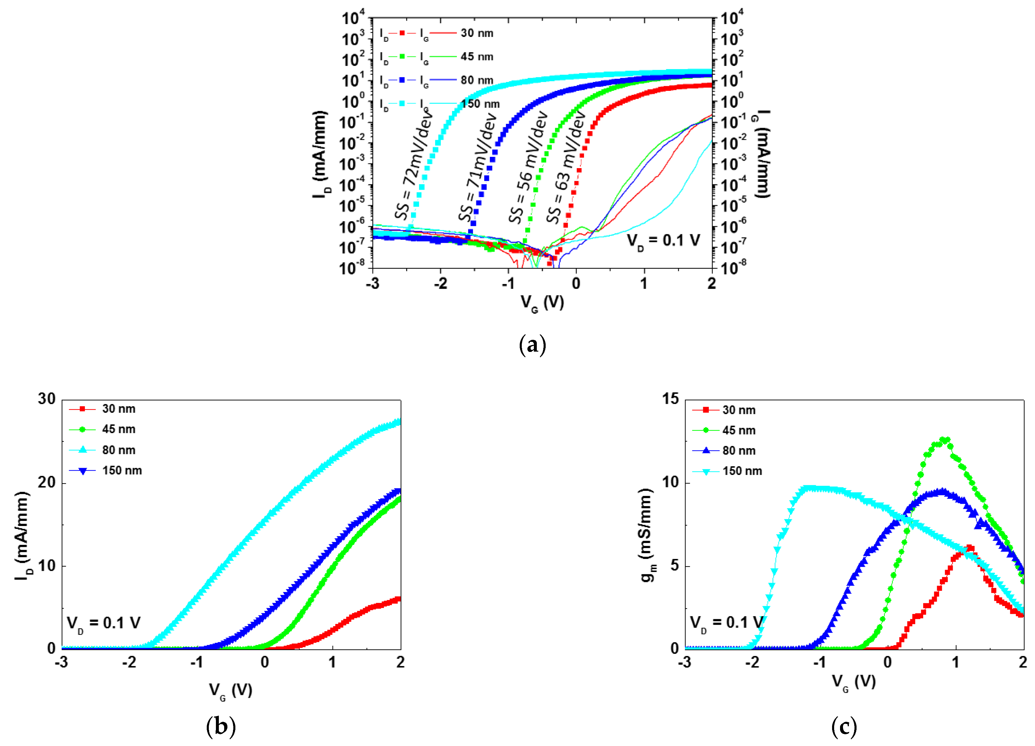
3. Results and Discussion

Figure 2a,b show the logarithmic and linear transfer curves, respectively, for the sloped sidewall AlGaN/GaN MIS-FinFETs with 20 nm-thick SiO2 gate dielectric varying the Wfin from 150 to 30 nm. The key parameters such as VTH, SS, gm peak value, full width at half maximum (FWHM) of gm, and hysteresis of all the devices are summarized and shown in Table 1. The VTH of the sloped FinFET with Wfin is 150 nm is −1.9 V and it shifts to a positive direction as the Wfin narrows, showing the VTH of 0.3 V when Wfin is reduced to 30 nm. This positive shift of the VTH is due to lateral depletion of the 2DEG channel from the sidewall. The SS values for all devices are smaller than 72 mV/dec, which are relatively low compared to those of conventional AlGaN/GaN-based HEMTs [21,22,23]. For the wide FinFETs with Wfin of 150 and 80 nm, the VTH of the 2DEG channel is much lower than that of the MOS channel at sidewall surface and hence the 2DEG channel current dominates the subthreshold current of the device. In this case, the SS (~ 70 mV/dec) for the device can be mainly determined from the trap capacitance at AlGaN/GaN interface (Cit,AlGaN/GaN) and the existence of the depletion capacitance (Cdep) in wide bottom fin body below the 2DEG channel, which is not completely depleted by the lateral electric field from the sidewall gate. Besides, the VTH difference between the 2DEG channel and MOS channel of these FinFETs with wide Wfin are relatively large and the two-channel currents become merged as the gate voltage increases to have the broad gm curves as shown in Figure 2c, which is important in improving the device linearity [8,24].
On the other hand, the narrow FinFET with Wfin of 45 nm has a sharper and higher gm peak as can be seen in Figure 2c, which means that the VTH of the 2DEG channel and MOS channel are almost the same and hence both channels simultaneously turn on/off and the effective channel width of the device can be modulated with the gate voltage, which results in very small SS as low as 56 mV/dec, smaller than the theoretical Boltzmann limit of 60 mV/dec. As discussed in our previous work [17], the 2DEG channel will be generated at the center of the 2DEG channel and laterally spread until occupying the whole 2DEG channel as VG increases from the VTH of the 2DEG channel to just above it. Then, the MOS channel will instantaneously turn on because there is only a tiny VTH difference between the top 2DEG channel and the sidewall MOS channel. In other words, the channel width first spread laterally within the 2DEG channel and then immediately spread vertically into the MOS channel, which makes the concept of gate-dependent effective channel width modulation reasonable. This sub-60 mV/dec SS can be understood by considering the expression for new S S W ( V G ) which includes the gate voltage-dependent channel width modulation [17] as shown below,
S S W ( V G ) = 1 d ( l o g I D , s u b ) d V G = 1 A + 1 S S c o n = S S c o n A   ·   1 S S c o n + 1
where d ( l o g I D , s u b ) d V G = d [ l o g W ( φ s ) ] d V G + d [ 0 V D Q c h ( V , φ s ) d V ] d V G + d ( l o g μ ) d V G , I D , s u b = μ W ( φ s ) L   0 V D Q c h ( V , φ s ) d V . In these equations,   φ s and Q c h ( V , φ s ) are the surface potential and the channel charges in the subthreshold region, respectively. W ( φ s ) is the surface potential-dependent effective channel width which is constant in conventional devices. I D , s u b   is the channel current in the subthreshold region and d ( l o g I D , s u b ) d V G is the differentiation of the logarithmic channel current. The first term d [ l o g W ( φ s ) ] d V G   in d ( l o g I D , s u b ) d V G is the channel width modulation and expressed as A in Equation (1). The third term is related to electron mobility and can be neglected. The inverse of the second term is S S c o n for conventional devices without channel width modulation. S S c o n   can be expressed as,
S S c o n = 2.3 k T q ( 1 + C d e p + C i t C o x )
where k is the Boltzmann’s constant, T is temperature, q is electronic charge, C o x is the capacitance for gate oxide, and C i t is the trap capacitance either for the interface of AlGaN/GaN or dielectric/GaN. Normally, S S c o n is larger than 60 mV/dec and cannot explain the sub-60 mV/dec characteristic observed in this work.
When Wfin is further reduced to 30 nm, the SS of the device increases slightly above 60 mV/dec again. This is because the VTH of the 2DEG channel increases and hence the simultaneous turning on of these two channels tends to break to make the channel width modulation less effective. The VTH of the 2DEG channel becomes higher than that of the MOS channel and becomes positive to show normally-off operation with VTH of 0.3 V. In this case, the MOS channel current at sidewall surface dominates the subthreshold characteristics of the device and the SS can be determined mainly from the trap capacitance ( C i t ,   S i O 2 / G a N ) at SiO2/GaN interface, which leads to increased SS of 63 mV/dec. As a result, Figure 2c indicates that the gm of the FinFET with Wfin of 30 nm becomes slightly broader and the peak value becomes lower again compared with that of FinFET with Wfin of 45 nm. As can be seen in Figure 2a, SS first decreases below 60 mV/dec when Wfin is reduced to 45 nm and then increases again above 60 mV/dec with further decreasing Wfin, which depends on whether the 2DEG channel and MOS channel turn on at the same time or not as has already been discussed above. Correspondingly, with decreasing Wfin, as shown in Figure 2c, gm curve becomes sharper as Wfin decreases to 45 nm, but becomes broad again when Wfin is reduced to 30 nm. Based on the tendency of SS and gm curves as decreasing Wfin as shown in Figure 2a,b, it can be concluded that the gm peak becomes sharp showing excellent subthreshold characteristics with SS of sub-60 mV/dec, if 2DEG channel and MOS channel of a FinFET are simultaneously turned on/off. However, most of the FinFETs with SiO2 dielectric layer investigated in this work exhibits normally-on operation, thus they are not adequate to be used as efficient power switching or low power logic application due to large IOFF, even though they exhibited excellent SS. A similar argument can be addressed even for the normally-off FinFET with Wfin of 30 nm, because IOFF of the FinFET is still very high due to its low VTH.
Figure 3a shows the comparison of the logarithmic transfer curves obtained from the FinFETs with sloped and steep sidewall surfaces. It is observed that the steep sidewall surface is m-plane and very smooth and uniform and has the lowest surface trap density, while the sloped sidewall has a rather rough and nonuniform surface, as shown in Figure 1b. The key parameters such as VTH, SS, gm peak value, and FWHM of gm of all the devices are summarized and shown in Table 2. Both devices, which have the same Wfin of 30 nm and 20 nm-thick SiO2 gate dielectric layer, exhibit normally-off operation, but the sloped sidewall device exhibits much higher IOFF of 100 nA/mm, measured at VG = 0 V, compared with that of steep sidewall device. The high IOFF of the sloped sidewall device is due to its lower VTH of 0.3 V, compared to VTH of 0.6 V of the steep sidewall device. The lower VTH of the sloped device is probably because the sidewall surface has a higher density of positive effective oxide charge at the GaN/SiO2 interface as well as higher surface trap density caused by a relatively rough surface, compared to the steep m-plane sidewall surface [25]. This high positive oxide charge density in the sloped device lowers VTH of the sidewall MOS channel to increase IOFF. The SS of steep sidewall device is as low as 37 mV/dec due to the simultaneous turning on of 2DEG channel and MOS channel and the effective channel width modulation as discussed before [17]. On the other hand, the sloped sidewall device exhibits a relatively larger SS of 63 mV/dec, which could be explained by the existence of non-negligible C d e p caused by the undepleted part at the wide fin bottom and relatively large C i t ,   S i O 2 / G a N due to a rough sidewall surface [25], which increases both S S c o n and S S W ( V G ) , while the C d e p can be ignored for the device with a steep sidewall because the entire fin is narrow and completely depleted from the electric field of the sidewall gate at off-state. The schematic images of both sloped and steep sidewall fin structures with un-depleted/depleted areas are shown in Figure 3b. The steep sidewall device exhibits a sharper and higher gm peak, as shown in Figure 3b, which indicates that both the 2DEG channel and the MOS channel of the device simultaneously turn on almost at the same time.
To investigate the effect of the gate dielectric on the device performances, the SiO2 layer was replaced with 10 nm-thick Al2O3 layers on the sloped sidewall FinFETs. All FinFETs with Wfin varied from 130 to 40 nm exhibit normally-off operation as shown in Figure 4a,b. The key parameters such as VTH, SS, gm peak value, FWHM of gm, and hysteresis of all the devices are summarized and shown in Table 3. Similarly, VTH of the FinFET shifts to a positive direction as Wfin decreases, but it increases up to a much higher value of 2.5 V for the FinFET with Wfin of 40 nm, which is probably due to the existence of the negative effective oxide charge at the interface between the Al2O3 dielectric layer and GaN [5,26,27].
It is also observed that the FinFETs show considerably low IOFF of ~ 0.1 nA/mm, except the FinFET with Wfin of 130 nm, which is essential for reducing the standby power consumption. Especially, the FinFET with Wfin of 40 nm exhibits excellent SS of 52 mV/dec, also smaller than the theoretically limited value of 60 mV/dec, which can be explained by the concept of effective channel width modulation and the simultaneous turn-on of 2DEG channel and MOS channel as discussed before. This fast switching characteristics of the device with its relatively high VTH of 2.5 V and low off-state leakage current would lead to improvement of efficiency and ensure the safety of power switching devices [28]. The gm peak becomes sharper as the Wfin of the FinFET decreases, as shown in Figure 4b, which is similar to the case of the FinFETs with SiO2 gate dielectric layer and a similar argument can be also addressed for the reason.
According to the discussion above, it can be seen that it is a possible method to realize relatively high VTH, small SS, and low IOFF in AlGaN/GaN MIS-FinFETs by carefully adjusting Wfin as well as choosing the sidewall plane, which corresponds to the controlling of threshold voltages. As Wfin varies, the shape of gm curve becomes sharper as the VTH difference between the 2DEG channel and the MOS channel becomes closer.

4. Conclusions

In this work, AlGaN/GaN MIS-FinFETs were fabricated and characterized using 20 nm-thick SiO2 and 10 nm-thick Al2O3 as dielectric layers, respectively. The effects of the sidewall plane on device performance were also investigated. The sloped sidewall FinFET with 20 nm-thick SiO2 dielectric layers and Wfin of 45 nm shows the lowest SS of 56 mV/dec among the FinFETs which can be explained by the concept of effective channel width modulation and the simultaneous turn-on of 2DEG channel and sidewall MOS channel. The SS is further decreased to 37 mV/dec for the steep sidewall FinFET with Wfin of 30 nm. However, the sloped sidewall FinFET with the same Wfin of 30 nm, which has a relatively rough sidewall surface, show low VTH, large SS, and high IOFF probably due to the high density of positive effective fixed oxide charges and trap charges at the SiO2/GaN interface. On the other hand, the sloped sidewall FinFETs with 10 nm-thick Al2O3 dielectric layer show normally-off operation with relatively high VTH, small SS, and low IOFF. In our opinion, these performances are probably due to the existence of negative effective fixed oxide charge at the Al2O3/GaN interface, even though the FinFETs have sloped sidewalls. The device with Wfin of 40 nm exhibits SS of 52 mV/dec with Vth of 2.3 V, which might be promising for efficient power switching application.

Author Contributions

Conceptualization, Q.D.; Formal analysis, Q.D. and J.-H.L.; Investigation, J.-H.L.; Methodology, Q.D.; Supervision, J.-H.L.; Writing—original draft, Q.D.; Writing—review & editing, J.-H.L. All authors have read and agreed to the published version of the manuscript.

Funding

This work was partly supported by the BK21 Plus funded by the Ministry of Education (21A20131600011) and this investigation was financially supported by Samsung Research Funding & Incubation Center of Samsung Electronics under Project Number SRFC-TA1703-08.

Conflicts of Interest

The authors declare no conflict of interest. The funders had no role in the design of the study; in the collection, analyses, or interpretation of data; in the writing of the manuscript, or in the decision to publish the results.

References

  1. Chen, K.J.; Häberlen, O.; Lidow, A.; Tsai, C.L.; Ueda, T.; Uemoto, Y.; Wu, Y. GaN-on-Si power technology: Devices and applications. IEEE Trans. Electron Devices 2017, 64, 779–795. [Google Scholar] [CrossRef]
  2. Khandelwal, S.; Chauhan, Y.S.; Fjeldly, T.A.; Ghosh, S.; Pampori, A.; Mahajan, D.; Dangi, R.; Ahsan, S.A. ASM GaN: Industry Standard Model for GaN RF and Power Devices—Part 1: DC, CV, and RF Model. IEEE Trans. Electron Devices 2019, 66, 80–86. [Google Scholar] [CrossRef]
  3. Flack, T.J.; Pushpakaran, B.N.; Bayne, S.B. GaN Technology for Power Electronic Applications: A Review. J. Electron Mater. 2016, 45, 2673–2682. [Google Scholar] [CrossRef]
  4. Tang, Z.; Jiang, Q.; Lu, Y.; Huang, S.; Yang, S.; Tang, X.; Chen, K.J. 600-V Normally off SiNx/AlGaN/GaN MIS-HEMT with large gate swing and low current collapse. IEEE Electron Device Lett. 2013, 34, 1373–1375. [Google Scholar] [CrossRef]
  5. Im, K.S.; Kim, R.H.; Kim, K.W.; Kim, D.S.; Lee, C.S.; Cristoloveanu, S.; Lee, J.H. Normally off single-nanoribbon Al2O3/GaN MISFET. IEEE Electron Device Lett. 2013, 34, 27–29. [Google Scholar] [CrossRef]
  6. Zhang, H.S.; Ma, X.H.; Zhang, M.; Lu, Y.; Zhu, Q.; Zhao, Z.Y.; Yi, C.P.; Yang, L.A.; Ma, P.J.; Hao, Y. Influence of Different Fin Configurations on Small-Signal Performance and Linearity for AlGaN/GaN Fin-HEMTs. IEEE Trans. Electron Devices 2019, 66, 3302–3309. [Google Scholar] [CrossRef]
  7. Zhu, M.; Ma, J.; Nela, L.; Erine, C.; Matioli, E. High-Voltage Normally-off Recessed Tri-Gate GaN Power MOSFETs with Low on-Resistance. IEEE Electron Device Lett. 2019, 40, 1289–1292. [Google Scholar] [CrossRef]
  8. Jo, Y.W.; Son, D.H.; Won, C.H.; Im, K.S.; Seo, J.W.; Kang, I.M.; Lee, J.H. AlGaN/GaN FinFET with Extremely Broad Transconductance by Side-Wall Wet Etch. IEEE Electron Device Lett. 2015, 36, 1008–1010. [Google Scholar] [CrossRef]
  9. Tamura, T.; Kotani, J.; Kasai, S.; Hashizume, T. Nearly Temperature-Independent Saturation Drain Current in a Multi-Mesa-Channel AlGaN/GaN High Electron Mobility Transistor. Appl. Phys. Express 2008, 1, 023001. [Google Scholar] [CrossRef] [Green Version]
  10. Ohi, K.; Asubar, J.T.; Nishiguchi, K.; Hashizume, T. Current Stability in Multi-Mesa-Channel AlGaN/GaN HEMTs. IEEE Trans. Electron Devices 2013, 60, 2997–3004. [Google Scholar] [CrossRef] [Green Version]
  11. Ohi, K.; Hashizume, T. Drain Current Stability and Controllability of Threshold Voltage and Subthreshold Current in a Multi-Mesa-Channel AlGaN/GaN High Electron Mobility Transistor. Jpn. J. Appl. Phys. 2009, 48, 081002. [Google Scholar] [CrossRef]
  12. Im, K.S.; Won, C.H.; Jo, Y.W.; Lee, J.H.; Bawedin, M.; Cristoloveanu, S.; Lee, J.H. High-performance GaN-based nanochannel FinFETs With/Without AlGaN/GaN heterostructure. IEEE Trans. Electron Devices 2013, 60, 3012–3018. [Google Scholar] [CrossRef]
  13. Choi, W.; Seok, O.; Ryu, H.; Cha, H.Y.; Seo, K.S. High-voltage and low-leakage-current gate recessed normally-Off GaN MIS-HEMTs with dual gate insulator employing PEALD-SiNx/RF-Sputtered-HfO2. IEEE Electron Device Lett. 2014, 35, 175–177. [Google Scholar] [CrossRef]
  14. Uemoto, Y.; Hikita, M.; Ueno, H.; Matsuo, H.; Ishida, H.; Yanagihara, M.; Ueda, T.; Tanaka, T.; Ueda, D. Gate Injection Transistor (GIT)—A Normally-Off Conductivity Modulation. IEEE Trans. Electron Devices 2007, 54, 3393–3399. [Google Scholar] [CrossRef]
  15. Ohmaki, Y.; Tanimoto, M.; Akamatsu, S.; Mukai, T. Enhancement-mode AlGaN/AlN/GaN high electron mobility transistor with low on-state resistance and high breakdown voltage. Jpn. J. Appl. Phys. 2006, 45, 1168–1170. [Google Scholar] [CrossRef]
  16. Huang, X.; Liu, Z.; Li, Q.; Lee, F.C. Evaluation and application of 600 V GaN HEMT in cascode structure. IEEE Trans. Power Electron. 2014, 29, 2453–2461. [Google Scholar] [CrossRef]
  17. Dai, Q.; Son, D.H.; Yoon, Y.J.; Kim, J.G.; Jin, X.; Kang, I.M.; Kim, D.H.; Xu, Y.; Cristoloveanu, S.; Lee, J.H. Deep Sub-60 mV/decade Subthreshold Swing in AlGaN/GaN FinMISHFETs with M-Plane Sidewall Channel. IEEE Trans. Electron Devices 2019, 66, 1699–1703. [Google Scholar] [CrossRef]
  18. Chu, Y.; Lu, S.C.; Chowdhury, N.; Povolotskyi, M.; Klimeck, G.; Mohamed, M.; Palacios, T. Superior Performance of 5-nm Gate Length GaN Nanowire nFET for Digital Logic Applications. IEEE Electron Device Lett. 2019, 40, 874–877. [Google Scholar] [CrossRef]
  19. Son, D.H.; Jo, Y.W.; Seo, J.H.; Won, C.H.; Im, K.S.; Lee, Y.S.; Jang, H.S.; Kim, D.H.; Kang, I.M.; Lee, J.H. Low voltage operation of GaN vertical nanowire MOSFET. Solid-State Electron. 2018, 145, 1–7. [Google Scholar] [CrossRef]
  20. Xu, Y.; Cristoloveanu, S.; Bawedin, M.; Im, K.S.; Lee, J.H. Performance Improvement and Sub-60 mV/Decade Swing in AlGaN/GaN FinFETs by Simultaneous Activation of 2DEG and Sidewall MOS Channels. IEEE Trans. Electron Devices 2018, 65, 915–920. [Google Scholar] [CrossRef]
  21. Hao, R.; Fu, K.; Yu, G.; Li, W.; Yuan, J.; Song, L.; Zhang, Z.; Sun, S.; Li, X.; Cai, Y.; et al. Normally-off p-GaN/AlGaN/GaN high electron mobility transistors using hydrogen plasma treatment. Appl. Phys. Lett. 2016, 109, 152106. [Google Scholar] [CrossRef]
  22. Song, B.; Zhu, M.; Hu, Z.; Qi, M.; Nomoto, K.; Yan, X.; Cao, Y.; Jena, D.; Xing, H.G. Ultralow-Leakage AlGaN/GaN High Electron Mobility Transistors on Si With Non-Alloyed Regrown Ohmic Contacts. IEEE Electron Device Lett. 2016, 37, 16–19. [Google Scholar] [CrossRef]
  23. Ahn, H.K.; Kim, H.C.; Kang, D.M.; Kim, S.L.; Lee, J.M.; Lee, S.H.; Min, B.G.; Yoon, H.S.; Kim, D.Y.; Lim, J.W.; et al. Effect of Fluoride-based Plasma Treatment on the Performance of AlGaN/GaN MISHFET. ETRI J. 2016, 38, 675–684. [Google Scholar]
  24. Zhang, K.; Kong, Y.; Zhu, G.; Zhou, J.; Yu, X.; Kong, C.; Li, Z.; Chen, T. High-Linearity AlGaN/GaN FinFETs for Microwave Power Applications. IEEE Electron Device Lett. 2017, 38, 615–618. [Google Scholar] [CrossRef]
  25. Matocha, K.; Tilak, V.; Dunne, G. Comparison of metal-oxide-semiconductor capacitors on c- and m-plane gallium nitride. Appl. Phys. Lett. 2007, 90, 123511. [Google Scholar] [CrossRef]
  26. Son, D.H.; Jo, Y.W.; Sindhuri, V.; Im, K.S.; Seo, J.H.; Kim, Y.T.; Kang, I.M.; Cristoloveanu, S.; Bawedin, M.; Lee, J.H. Effects of sidewall MOS channel on performance of AlGaN/GaN FinFET. Microelectron. Eng. 2015, 147, 155–158. [Google Scholar] [CrossRef]
  27. Jo, Y.W.; Son, D.H.; Won, C.H.; Sindhuri, V.; Kim, J.H.; Seo, J.H.; Kang, I.M.; Lee, J.H. Control of Transconductance in High Performance AlGaN/GaN FinFETs. In Proceedings of the IEEE 11th International Conference on Power Electronics and Drive Systems, Sydney, Australia, 9–12 June 2015. [Google Scholar]
  28. Lu, B. AlGaN/GaN-Based Power Semiconductor Switches. Ph.D. Thesis, Massachusetts Institute of Technology, Cambridge, MA, USA, June 2013. [Google Scholar]
Figure 1. (a) Schematic image of AlGaN/GaN-based FinFET with either sloped sidewall surface or steep sidewall surface; (b) Cross-sectional TEM image of fin with sloped sidewall surface; (c) Cross-sectional TEM image of fin with steep sidewall surface.
Electronics 09 01967 g001
Figure 2. Sloped sidewall MIS-FinFETs with 20 nm-thick SiO2 gate dielectric varying the Wfin from 150 to 30 nm. (a) Logarithmic transfer curves; (b) Linear transfer curves; (c) Transconductance curves.
Electronics 09 01967 g002
Figure 3. (a) Logarithmic transfer curves of sloped sidewall FinFETs (red line) in this work and steep sidewall FinFETs (black line) in our previous work; (b) Transfer curves of the two devices in (a). The schematic images of sloped and steep sidewall fin structures are shown in the insert of (b).
Electronics 09 01967 g003
Figure 4. Sloped sidewall MIS-FinFETs with 10 nm-thick Al2O3 gate dielectric varying the Wfin from 130 to 40 nm. (a) Logarithmic transfer curves; (b) Linear transfer curves; (c) Transconductance curves.
Electronics 09 01967 g004
Table 1. Key parameters for each device exhibited in Figure 2.
Wfin (nm)VTH (V)SS (mV/dec)gm Peak (mS/mm)FWHM of gm (V)Hysteresis (mV)
300.3636.10.92400
45−0.25412.61.52320
80−0.9719.52.40240
150−1.9729.83.12120
Table 2. Key parameters for each device exhibited in Figure 3.
Wfin (nm)Sidewall TypeVTH (V)SS (mV/dec)gm Peak (mS/mm)FWHM of gm (V)
30sloped0.3636.10.92
30steep0.63715.60.60
Table 3. Key parameters for each device exhibited in Figure 4.
Wfin (nm)VTH (V)SS (mV/dec)gm Peak (mS/mm)FWHM of gm (V)Hysteresis (mV)
402.352170.88400
501.86119.51.04480
1000.86313.92.12400
13006814.42.44400
Publisher’s Note: MDPI stays neutral with regard to jurisdictional claims in published maps and institutional affiliations.

