Article

Numerical Study of Sub-Gap Density of States Dependent Electrical Characteristics in Amorphous In-Ga-Zn-O Thin-Film Transistors

1
School of Electronic and Electrical Engineering, Kyungpook National University, 80 Daehakro, Bukgu, Daegu 41566, Korea
2
College of Ocean Science and Engineering, Shandong University of Science and Technology, Qingdao 266590, China
3
Department of Electronic Engineering, Hallym University, Chuncheon 24252, Korea
4
School of Electronics Engineering, Kyungpook National University, 80 Daehakro, Bukgu, Daegu 41566, Korea
*
Authors to whom correspondence should be addressed.
Electronics 2020, 9(10), 1652; https://doi.org/10.3390/electronics9101652
Submission received: 14 September 2020 / Revised: 5 October 2020 / Accepted: 6 October 2020 / Published: 11 October 2020
(This article belongs to the Section Semiconductor Devices)

Abstract

:
We demonstrate the effect of the sub-gap density of states (DOS) on electrical characteristics in amorphous indium-gallium-zinc (IGZO) thin-film transistors (TFTs). Numerical analysis based on a two-dimensional device simulator Atlas controlled the sub-gap DOS parameters such as tail acceptor-like states, tail donor-like states, Gauss acceptor-like states, and Gauss donor-like states in amorphous IGZO TFTs. We confirm accuracy by exploiting physical factors, such as oxygen vacancy, peroxide, hydrogen complex, band-to-band tunneling, and trap-assisted tunneling. Consequently, the principal electrical parameters, such as the threshold voltage, saturation mobility, sub-threshold swing, and on-off current ratio, are effectively tuned by controlling sub-gap DOS distribution in a-IGZO TFTs.

Graphical Abstract

1. Introduction

Thin-film transistors (TFTs) have received significant attention because of the rapid development of displays, sensors, computing, radiofrequency tags, and analog signal processing [1,2,3,4,5,6]. Specifically, TFTs based on metal-oxide, organic, and low-dimensional materials have advanced, achieving high electrical performances, optical transparency, and mechanical flexibility [7,8,9,10]. Among the various next-generation material-based TFTs, amorphous oxide semiconductor (AOS) TFTs based on multi-components exhibit high uniformity because of their high mobility, amorphous phase, and high transparency and flexibility [11,12,13]. Indium-gallium-zinc (IGZO) TFTs are the most representative AOS TFTs because of the advantages of carrier concentration controllability, electrical characteristics stability, and process compatibility with present fabrication [14,15,16]. A challenging issue in IGZO TFTs is enhancing electrical performance to drive high-quality active-matrix electronics, such as organic light-emitting diodes, micro light-emitting diodes, and high-resolution displays and sensors. To enhance the electrical performance of IGZO TFTs, many studies on IGZO TFTs exist, and oxygen vacancy (OV), peroxide (PO), and hydrogen complex (HC) models have been suggested [17,18,19,20]. However, progress has been insufficient to fully understand the change of electrical characteristics induced by the sub-gap density of states (DOS), even though sub-gab DOS distributions are highly related to the electrical characteristics of AOS TFTs.
In this study, we controlled sub-gap DOS distribution in variables such as tail acceptor-like states (NTA), tail donor-like states (NTD), Gauss donor-like states (NGA), and Gauss acceptor-like states (NGD). Therefore, we use Silvaco’s two-dimensional device simulator Atlas to examine the effect of sub-gab DOS distributions on electrical characteristics. Consequently, the results show that the characteristics of electrical parameters, such as the threshold voltage (Vth), saturation mobility (μsat), sub-threshold swing (S), and on-off current ratio (Ion/Ioff), significantly affect the sub-gap DOS distribution.

2. Simulation Methodology

For the AOS IGZO TFT simulation, top-contact bottom-gate staggered structure was used in this study (Figure 1a). In the simulation, indium tin oxide (ITO) and aluminum (Al) were used for the gate and the source and drain electrodes, respectively. The work functions of ITO and Al are 4.7 eV and 4.33 eV, respectively. The lengths of both source and drain are 1 µm, and the gate length is 10 µm. The thickness of the electrodes is 50 nm. The gate insulator is a 100-nm-thick SiO2, and the active layer material is IGZO. The channel width and length are 100 µm and 10 µm, respectively. The affinity and bandgap of the IGZO parameters are 4.16 eV and 3.05 eV, respectively, and the conduction band (NC) and valence band (NV) effective DOS are calculated using Equations (1) and (2).
N C = 2 ( 2 π M C k t h 2 ) 3 2 ,
N V = 2 ( 2 π M V k t h 2 ) 3 2 ,
In this study, we assumed that the effective mass of the electron and hole are 0.34 MO and 21 MO [21]. The values calculated using Equations (1) and (2) are 5 × 1018 cm−3 eV−1 and 2.4 × 1021 cm−3 eV−1, respectively. This study assumed that localized states and NGD are equal. We also assumed that the electron carrier concentration is partially ionized from NGA using the OV model. Figure 1b presents the reference sub-gap DOS consisting of NTA, NTD, NGA, and NGD. Each formula follows the sub-gap DOS model [21]. The NTA distribution equation (GTA (E)) in the sub-gap DOS is (3).
G T A ( E ) = N T A e ( E E C ) W T A ,
where E is the electron energy, EC is the conduction band edge energy, NTA is the sub-gap DOS at E−EC, and WTA is the characteristic decay energy. The NTD distribution equation (GTD (E)) in the sub-gap DOS is given by Equation (4).
G T D ( E ) = N T D e ( E V E ) W T D ,
where EV is the valence band edge energy, NTD is the sub-gap DOS at E−EV, and WTD is the characteristic decay energy. The NGA distribution equation (GGA (E)) in the sub-gap DOS is given by Equation (5).
G G A ( E ) = N G A e [ ( ( E E G A ) W G A ) 2 ] ,
where EGA is the NGA energy peak, NGA is the Gaussian acceptor-like states at EGAE in the sub-gap DOS, and WGA is the characteristic decay energy. The NGD distribution equation (GGD (E)) in the sub-gap DOS is given by Equation (6).
G G D ( E ) = N G D e [ ( ( E E G D ) W G D ) 2 ] ,
where EGD is the NGD energy peak, NGD is Gaussian donor-like states at EEGD in the sub-gap DOS, and WGD is the characteristic decay energy. In the semiconductor based on Si and compound case, NGD is located near EV, but in the AOS case, NGD is positioned near EC because the NGD position changes the Madelung potential effect of the OV model [17].
The OV model demonstrates the NGD moves from a deep trap state to localized states because of the Madelung potential. Furthermore, the electrons are generated by removing oxygen bonding. The OV model is associated with Equation (7).
V O X V O + 2 + 2 e ,
where the neutrality charge is X, the two-plus charge is +2, the OV state is VO, and e is the electron. Therefore, the VO state level is changed by filling or discharging electrons using the Madelung potential. Therefore, NGD would change from deep trap states to localized states. Furthermore, the PO model shows that excess oxygen induces an O–O bonding and identifies changed localized state levels. Thus, the NGD energy level should change in the localized state regime under the PO model [18]. Furthermore, the HC model illustrates that coupling metal atoms and light hydrogen atoms induces various energy levels [19]. Consequently, coupling at various energy levels would change the sub-gap DOS and Fermi level. Therefore, these variable models should demonstrate varying sub-gaps DOS by chemical atomic bonding or breaking. Thus, various parameters in the sub-gap DOS using the models should be applied in the simulation to observe the changes in the electrical characteristics in this study. Table 1 shows other parameters required for simulation. For accurate simulation, the generation-recombination mechanisms tarp-assisted tunneling (TAT) associated with band-to-band (BBT) and Pool–Frenkel Barrier Lowering (PFBL) models must be used [21,22]. The BBT and TAT models [23] should change the generation rate.
G B B T ( F ) = q 2 F 2 m r 1 2 18 π E G 1 2 e ( π m r 1 2 E G 3 2 2 q F ) ,
F, mr, q, and EG are the local electric field, conduction band effective mass, elementary charge, and bandgap energy, respectively.

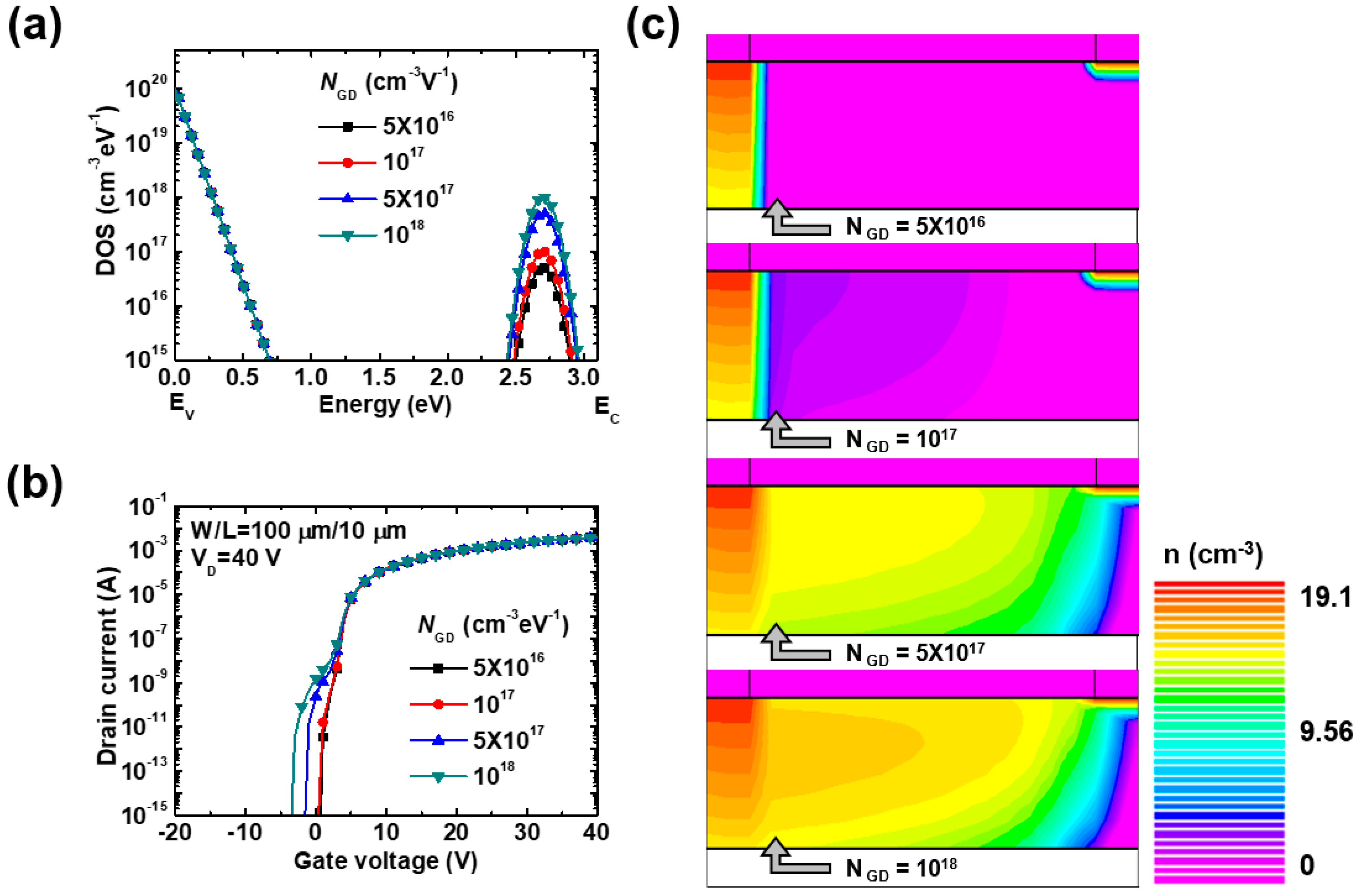
3. Results and Discussion

Figure 2a shows the NTA versus energy (E). The NTA varies from 1 × 10¹⁸ to 5 × 1019 cm−3 eV−1 by five intervals. Figure 2b shows that the transfer curve is changing with the NTA. It presents the log scaled IDVG curve by sweeping VG from −20 V to 40 V at VD = 40 V of a-IGZO TFTs from each NTA. Thus, electrical performance such as low Ion/Ioff from 5 × 10¹² to 2.27 × 10¹² A and low μsat from 11–7.9 cm2 V−1·s−1, high Vth from 0.35–4.5 V, and high S from 128–438 mV dec−1 would be worse. We extract electrical parameters by analyzing the transfer curves. We take advantage of specific equations to extract parameters. First, ID is given by Equation (6) at the saturation region in the IDVG transfer curve.
I D = μ s a t · C o x ( W 2 L ) ( V G V t h ) 2 ,
where W is the device width, L is the channel length, and Cox is the semiconductor insulator. Second, the G r a d . m a x of the maximum gradient concept is used to extract μsat and Vth at the saturation region in the I D VG transfer curve.
G r a d = a I D a V G = ( μ s a t · C o x ( W 2 L ) ) 1 2 .
G r a d . m a x is the maximum gradient value. Furthermore, to evaluate the device performance, the Ion/Ioff is critical at the saturation region in the IDVG transfer curve.
I o n I o f f = I D | V G = 40 V I D | V G = 20 V .
Third, μsat is critical for evaluating device performance in the IDVG transfer curve at the saturation region in the I D VG transfer curve.
  μ s a t = ( 1 C o x ) ( 2 L W ) ( G r a d . m a x ) 2 .
Fourth, Vth is also necessary for evaluating device performance in the IDVG transfer curve at the saturation region in the I D VG transfer curve.
V t h =   V G - I D G r a d . m a x .
Fifth, S is concerned with the low power device parameter at the saturation region in the IDVG transfer curve.
S = a V G a log ( I D ) = 1 μ s a t · C o x ( W 2 L ) .
Finally, the concept of Von should be used to evaluate the changing electrical property exactly at the saturation region in the IDVG transfer curve. Note that these phenomena are matched to the multiple trapping and release (MTR) model [24]. Thus, many NTA would interfere with the path of the electron. We elucidate the reasons by investigating the electron concentration distribution in the channel (Figure 2c). The results show that NTA is associated with lowering the electron concentration from top to bottom in the channel because of trapping electrons. Therefore, the NTA would be disturbed to move electrons using the MTR effect. Furthermore, we also ran the simulation in relation to WTA. The variation of WTA is 0.08–0.14 eV at NTA = 1018 cm−3 eV−1. However, no change in electrical properties was observed in this study. Therefore, NTA is more important than WTD regarding its effect on electrical performance.
Figure 3a shows the NGAE. The variation of NGA is from 1016 to 5 × 10¹⁷ by five intervals. Figure 3b shows that the transfer curve is changing with NGA. It presents the log scaled IDVG curve by sweeping VG from −20 V–40 V at VD = 40 V of IGZO TFTs from each NGA. Therefore, electrical performance, such as low Ion/Ioff from 4 × 10¹² to 2.93 × 10¹² A and low μsat from 10.4 to 9.8 cm2 V−1·s−1, high Vth from 0.5 to 2.5 V, high Von from 0.5 to 2.5 V, and high S from 128 to 316 mV dec−1, would be worse. Thus, this work investigates some electrical properties. First, both NTA and NGA negatively affect electrical performance under the MTR model. Second, the NTA significantly changes the Ion/Ioff. However, the NGA significantly changes the positive shift Vth. If we employ the NTA in this study, the acceptor-like traps should increase around the end of the EC. Therefore, the electrons should be trapped and released more easily by the NTA around the end of the EC when the device is operated. However, if we employ the NGA in this study, the acceptor-like traps increase around the EGA because NGA is not located at the edge of EC. This means that electrons are trapped in acceptor-like states, but in the NGA case, electrons must have more energy to be emitted because they are not located near EC when the device is operated. Finally, other condition studies also run simulations of parameters, such as WGA and EGA, with ranges of 0.05Ѿ0.3 eV at NGA = 5 × 1016 cm−3 eV−1 and 0.3–0.6 eV in ECE at NGA = 5 × 1016 cm−3 eV−1. However, these did not change the electrical performance. The results show that it is critical to reduce the amount of NTA and adjust the EGA control position for making high-performance AOS IGZO TFTs. We also simulated the NTD and WTD in the sub-gap DOS, ranging from 5 × 10¹⁸ to 1020 cm−3 eV−1 and 0.03 to 0.06 eV at NTD = 1020 cm−3 eV−1. However, these did not change the electrical performance because, in this case, the IGZO channel layer is a large bandgap and NTD is far from the EC point. Therefore, the NTD near EV does not affect electrical performance when the device is operated. However, if high energy is injected, such as photons, it should release electrons in the states, and the electrons released from NTD to EC should change the electrical performance [25].
Figure 4a shows the NGDE. The range of NGD is from 5 × 10¹⁶ to 1018 cm−3 eV−1 by five intervals. Figure 4b shows the transfer curve changes with NGD. It shows sweeping VG from −20 to 40 V at VD = 40 V of IGZO TFTs from each NGA. Thus, the electrical performances, such as low Von from 0.85 to −3.4 V, and high S from 172 to 744 mV dec−1, would be better and worse, respectively. Note that the distribution of NGD affects the electrical performance, such as a bad S and negative-shift Vth. Therefore, NGD is related to trapping electrons and associated with electron generation in the channel more easily by VO. Therefore, if the NGD increases, S deteriorates, and Vth changes in a negative shift. We elucidate more detailed reasons by examining the electron concentration distribution (Figure 4c). From the top to the bottom pictures, we find that the electrons gathered more easily on the channel by the condition NGD at the saturation region of the simulated IGZO TFTs VD = 40 V and VG = 0 V. Note that these results illustrate a tendency by the OV model. Therefore, the oxygen concentration must be controlled, and the NGD level via the PO and OV models must be adjusted.
Figure 5a shows the EGDE. The range of EGD is from 2.3–2.9 eV for the ECE. Figure 5b shows that the transfer curve is changing with EGD. It presents by sweeping VG −20 to 40 V at VD = 40 V of IGZO TFTs from each EGD. The electrical performances, such as high Ion/Ioff from 3.7 × 10¹² to 3.9 × 10¹² A and high μsat from 9.9 to 10.4 cm2 V−1·s−1, low Vth from 4.9 to 3.2 V, low Von from 0 to −2.2 V, and low S from 407 to 152 mV dec−1, are shown. As the EGD approaches EC, the electrical performances are improved, but the slope of the transfer curve changes around 0 V, showing a non-ideal transfer characteristic. Therefore, optimized electrical characteristic requires moving up by controlling the localized states in donor-like states by O–O bonding and VO. For elucidating more detailed reasons, we investigated, as shown in Figure 5c. From the top to the bottom pictures, we find that the carrier concentration in the channel is high because EGD is located near EC more closely at VG = 0 V and VD = 40 V. Therefore, EGD is concerned with the carrier injection as a doping semiconductor by VO. Therefore, when EGD is located near EC, electrons are generated more easily. Therefore, the electrons are released rather than trapped, and the electrical performance could be improved.

4. Conclusions

We have described the importance of key parameters of acceptor-like and donor-like states in sub-gap states. From the simulation model and related theories, this work clarified how the sub-gap DOS profile affects the electrical characteristics in the a-IGZO TFTs. Note that four controlled variables, namely, NTA, NGA, NGD, and EGD, significantly affected electrical performances such as Von, Vth, S, Ion/Ioff, and μsat. For acceptor-like traps, all electrical properties became worse because of the trapped electrons near the EC base on the MTR effect. For donor-like traps, some electrical properties such as S became worse because of localized states. Other electrical properties such as Vth and μsat improved because of the injected electrons based on the OV and PO models. In the future, we want to investigate the effect of more than four variables focused on in this work on electrical properties to exactly determine the significant role of controlling parameters on the improvement of the electrical properties in AOS TFTs.

Author Contributions

D.-K.K., J.-H.B. designed the research. D.-K.K. and J.P. (Jihwan Park) conducted simulation. D.-K.K., J.P. (Jihwan Park) and X.Z. analyzed the data and wrote the manuscript. J.P. (Jaehoon Park) and J.-H.B. edited the manuscript. All authors reviewed the manuscript. Project administration was conducted by J.P. (Jaehoon Park) and J.-H.B. All authors have read and agreed to the published version of the manuscript.

Funding

This research was funded by the Basic Science Research Program through the National Research Foundation of Korea (NRF) funded by the Ministry of Science and ICT (2018R1A2B6008815). The research was also supported by Hallym University Research Fund, 2020 (HRF-202009-015).

Conflicts of Interest

The authors declare no conflict of interest.

References

  1. Lee, W.; Someya, T. Emerging trands in flexible active multielectrode arrays. Chem. Mater. 2019, 31, 6347–6358. [Google Scholar] [CrossRef]
  2. Nela, L.; Tang, J.; Cao, Q.; Tulevski, G.; Han, S.-J. Large-Area High-Performance Flexible Pressure Sensor with Carbon Nanotube Active Matrix for Electronic Skin. Nano Lett. 2018, 18, 2054–2059. [Google Scholar] [CrossRef] [PubMed]
  3. Jang, J.; Oh, B.; Jo, S.; Park, S.; An, H.S.; Lee, S.; Cheong, W.H.; Yoo, S.; Park, J.-U. Human-Interactive, Active-Matrix Displays for Visualization of Tactile Pressures. Adv. Mater. Technol. 2019, 4, 1900082. [Google Scholar] [CrossRef]
  4. Hills, G.; Lau, C.; Wright, A.; Fuller, S.; Bishop, M.D.; Srimani, T.; Kanhaiya, P.; Ho, R.; Amer, A.; Stein, Y.; et al. Modern microprocessor built from complementary carbon nanotube transistors. Nature 2019, 572, 595–602. [Google Scholar] [CrossRef]
  5. Myny, K.; Lai, Y.-C.; Papadopoulos, N.; Roose, F.D.; Ameys, M.; Willegems, M.; Smout, S.; Steudel, S.; Dehaene, W.; Genoe, J. A Flexible ISO14443-A Compliant 7.5mW 128b Metal-Oxide NFC Barcode Tag with Direct Clock Division Circuit from 13.56MHz Carrier. In Proceedings of the IEEE International Solid-State Circuits Conference (ISSCC), San Francisco, CA, USA, 5–9 February 2017; pp. 258–259. [Google Scholar]
  6. Pecunia, V.; Fattori, M.; Abdinia, S.; Sirringhaus, H.; Cantatore, E. Organic and Amorphous-Metal-Oxide Flexible Analogue Electronics; Cambridge University Press: Cambridge, UK, 2018. [Google Scholar]
  7. Choi, S.; Lee, H.; Ghaffari, R.; Hyeon, T.; Kim, D.-H. Recent Advances in Flexible and Stretchable Bio-Electronic Devices Integrated with Nanomaterials. Adv. Mater. 2016, 28, 4203–4218. [Google Scholar] [CrossRef]
  8. Trung, T.-Q.; Lee, N.-E. Materials and devices for transparent stretchable electronics. J. Mater. Chem. C 2017, 5, 2202–2222. [Google Scholar] [CrossRef]
  9. Sharma, B.K.; Ann, J.-H. Flexible and Stretchable Oxide Electronics. Adv. Electron. Mater. 2016, 2, 1600105. [Google Scholar] [CrossRef]
  10. Diao, Y.; Tee, B.C.-K.; Giri, G.; Xu, J.; Kim, D.H.; Becerril, H.A.; Stoltenberg, R.M.; Lee, T.H.; Xue, G.; Mannsfeld, S.C.B.; et al. Solution coating of large-area organic semiconductor thin films with aligned single-crystalline domains. Nat. Mater. 2013, 12, 665–671. [Google Scholar] [CrossRef]
  11. Jang, J.; Kitsomboonloha, R.; Swisher, S.L.; Park, E.S.; Kang, H.; Subramanian, V. Transparent High-Performance Thin Film Transistors from Solution-Processed SnO2/ZrO2 Gel-like Precursors. Adv. Mater. 2012, 25, 1042–1047. [Google Scholar] [CrossRef]
  12. Fortunato, E.; Barquinha, P.; Martins, R. Oxide Semiconductor Thin-Film Transistors: A Review of Recent Advances. Adv. Mater. 2012, 24, 2945–2986. [Google Scholar] [CrossRef]
  13. Petti, L.; Muenzenrieder, N.; Vogt, C.; Faber, H.; Buethe, L.; Cantarella, G.; Bottacchi, F.; Anthopoulos, T.D.; Troester, G. Metal oxide semiconductor thin-film transistors for flexible electronics. Appl. Phys. Rev. 2016, 3, 021303. [Google Scholar] [CrossRef] [Green Version]
  14. Kamiya, T.; Hosono, H. Material characteristics and applications of transparent amorphous oxide semiconductors. NPG Asia Mater. 2010, 2, 15–22. [Google Scholar] [CrossRef] [Green Version]
  15. Tak, Y.J.; Yoon, D.H.; Yoon, S.; Choi, U.H.; Sabri, M.M.; Ahn, B.D.; Kim, H.J. Enhanced Electrical Characteristics and Stability via Simultaneous Ultraviolet and Thermal Treatment of Passivated Amorphous In–Ga–Zn–O Thin-Film Transistors. ACS Appl. Mater. Interfaces 2014, 6, 6399–6405. [Google Scholar] [CrossRef] [PubMed]
  16. Jo, J.-W.; Kim, J.; Kim, K.-T.; Kang, J.-G.; Kim, M.-G.; Kim, K.-H.; Ko, H.; Kim, Y.-H.; Park, S.K. Highly Stable and Imperceptible Electronics Utilizing Photoactivated Heterogeneous Sol-Gel Metal–Oxide Dielectrics and Semiconductors. Adv. Mater. 2015, 27, 1182–1188. [Google Scholar] [CrossRef] [PubMed]
  17. Janotti, A.; Van de Walle, C.G. Native point defects in ZnO. Phys. Rev. B 2007, 76, 165202. [Google Scholar] [CrossRef]
  18. Nahm, H.H.; Kim, Y.S.; Kim, D.H. Instability of amorphous oxide semiconductors via carrier-mediated structural transition between disorder and peroxide state. Phys. Status Solidi B 2012, 249, 1277–1281. [Google Scholar] [CrossRef]
  19. Kang, Y.; Ahn, B.D.; Song, J.H.; Mo, Y.G.; Nahm, H.H.; Han, S.; Jeong, J.K. Hydrogen Bistability as the Origin of Photo-Bias-Thermal Instabilities in Amorphous Oxide Semiconductors. Adv. Electron. Mater. 2015, 1, 1400006. [Google Scholar] [CrossRef]
  20. Park, J.-H.; Kim, D.-K.; Park, J.-I.; Kang, I.M.; Jang, J.; Kim, H.; Lang, P.; Bae, J.-H. Numerical analysis on effective mass and traps density dependence of electrical characteristics of a-IGZO thin-film transistors. Electronics 2020, 9, 119. [Google Scholar] [CrossRef] [Green Version]
  21. Takagi, A.; Nomura, K.; Ohta, H.; Yanagi, H.; Kamiya, T.; Hirano, M.; Hosono, H. Carrier transport and electronic structure in amorphous oxide semiconductor, a-InGaZnO4. Thin Solid Films 2005, 486, 38–41. [Google Scholar] [CrossRef]
  22. Altas User’s Manual; Silvaco Inc.: Santa Clara, CA, USA, 2016.
  23. Wakimura, G.; Yamauchi, Y.; Kamakura, Y. Simulation and modeling of off-leakage current in InGaZnO thin-film transistors. J. Adv. Simulat. Sci. Eng. 2015, 2, 201–210. [Google Scholar] [CrossRef] [Green Version]
  24. Lee, S.; Ghaffarzadeh, K.; Nathan, A.; Robertson, J.; Jeon, S.; Kim, C.; Song, I.-H.; Chung, U.I. Trap-limited and percolation conduction mechanisms in amorphous oxide semiconductor thin film transistors. Appl. Phys. Lett. 2011, 98, 203508. [Google Scholar] [CrossRef]
  25. Ryu, B.; Noh, H.K.; Choi, E.A.; Chang, K.J. O-vacancy as the origin of negative bias illumination stress instability in amorphous In–Ga–Zn–O thin film transistors. Appl. Phys. Lett. 2010, 97, 022108. [Google Scholar] [CrossRef] [Green Version]
Figure 1. (a) Schematic cross-sectional view of the structure of the bottom-gate staggered structure of the device used in this work. (b) Density of states (DOS) is shown as a function of energy (E). The black squares are total acceptor-like traps sub-gap DOS, and the red circles are total donor-like traps sub-gap DOS.
Electronics 09 01652 g001
Figure 2. (a) Density of states (DOS) in sub-gap is shown as a function of energy. The tail acceptor-like states (NTA) are controlled from 1018 to 5 × 1019 cm−3 eV−1. (b) Drain current according to the applied gate voltage is shown at 40 V of drain voltage. (c) Each layer depicts the electron concentration distribution from top to bottom of NTA in the range of 1018 to 5 × 1019 cm−3 eV−1 at the saturation region 40 V of gate voltage, and 40 V of drain voltage. The color table displays the electron concentration variations of 0–1019.1 in varying colors.
Electronics 09 01652 g002
Figure 3. (a) DOS in sub-gap is shown as a function of energy. The Gauss donor-like states (NGA) are controlled from 1016 to 5 × 1017 cm−3 eV−1. (b) Drain current according to applied gate voltage is shown at 40 V of drain voltage. (c) Each layer depicts the electron concentration distribution from top to bottom of NGA ranging from 1016 to 5 × 1017 cm−3 eV−1 at the saturation region 40 V of gate voltage and 40 V of drain voltage. The color table displays the electron concentration variations of 0–1019.1 in varying colors.
Electronics 09 01652 g003
Figure 4. (a) DOS in sub-gap is shown as a function of energy. The Gauss acceptor-like states (NGD) are controlled from 5 × 10¹⁶ to 1018 cm−3 eV−1. (b) Drain current according to applied gate voltage is shown at 40 V of drain voltage. (c) Each layer depicts the electron concentration distribution from top to bottom of NGD ranging from 5 × 10¹⁶ to 1018 cm−3 eV−1 at the saturation region 40 V of gate voltage and 40 V of drain voltage. The color table displays the electron concentration variations of 0–1019.1 in varying colors.
Electronics 09 01652 g004
Figure 5. (a) DOS in sub-gap is shown as a function of energy. The EGD is controlled from 2.3–2.9. (b) Drain current according to applied gate voltage is shown at 40 V of drain voltage. (c) Each layer depicts the electron concentration distribution from top to bottom of NGD ranging from 2.3–2.9 eV at the saturation region 40 V of gate voltage and 40 V of drain voltage. The color table displays the electron concentration variations of 0–1019.1 in varying colors.
Electronics 09 01652 g005
Table 1. Simulation parameters for the a-indium-gallium-zinc (IGZO) thin-film transistors (TFTs).
ParameterValueUnitDescription
µn15cm2 V−1·s−1Electron mobility
µp0.1cm2 V−1·s−1Hole mobility
NTA1 × 1018cm−3 eV−1Density of tail states at conduction band
NTD1 × 1020cm−3 eV−1Density of tail states at valence band
NGD5 × 1016cm−3 eV−1Density of Gauss donor-like states
NGA5 × 1016cm−3 eV−1Density of Gauss acceptor-like states
WTA0.08eVCharacteristic decay energy of acceptor-like tail states
WTD0.06eVCharacteristic decay energy of donor-like tail states
WGD0.1eVCharacteristic decay energy of donor-like Gauss states
WGA0.2eVCharacteristic decay energy of acceptor-like Gauss states
EGD2.7eVEnergy corresponding to the peak for donor-like Gauss states
EGA0.5eVEnergy corresponding to the peak for acceptor-like Gauss states
NC5 × 1018cm−3 eV−1Effective density of states for conduction band
NV2.4 × 1021cm−3 eV−1Effective density of states for valance band
EG3.05eVEnergy band
Xe4.16eVElectron affinity
MC0.34 MoKgEffective mass of conduction band
MV21 MoKgEffective mass of valence band
ɛs10ɛoFm−1Dielectric constant
n1015cm−3Electron carrier concentration

