Article

A Novel Dual Integrated LLC Resonant Converter Using Various Switching Patterns for a Wide Output Voltage Range Battery Charger

Department of Electrical and Computer Engineering, Sungkyunkwan University, Suwon 16419, Korea
*
Author to whom correspondence should be addressed.
Electronics 2019, 8(7), 759; https://doi.org/10.3390/electronics8070759
Submission received: 12 June 2019 / Revised: 1 July 2019 / Accepted: 4 July 2019 / Published: 6 July 2019
(This article belongs to the Special Issue Advanced Power Conversion Technologies)

Abstract

:
This paper proposes a novel dual integrated LLC resonant converter (DI-LRC) with a wide output voltage range using various switching patterns. The primary side of the proposed DI-LLC converter consists of two resonant tanks and six switches, while the secondary side consists of a six-pulse diode rectifier. Depending on the switching pattern of the primary switch, the DI-LRC converter is performed by single full-bridge operation with a voltage gain of 1, series-connected full-bridge operation with a voltage gain of 0.5, series-connected half bridge operation with a voltage gain of 0.25, and parallel-connected full-bridge operation with a voltage gain of 2. Accordingly, the proposed DI-LRC converter has four voltage gain curves with different variations and achieves a wider output voltage range than the conventional single voltage gain curve in a given operating frequency range. In this paper, the equivalent circuits derived for each switching pattern are proposed to analyze the operating characteristics of the proposed converter according to each switching pattern, and each Q factor and voltage gain are calculated based on the analyzed equivalent circuit. The performance of the proposed converter and switching pattern is verified using the simulation and experimental results of the prototype battery charger, which is designed to be 4-kW class.

1. Introduction

Recently, the LLC resonant converter with high soft-switching performance, high efficiency, and high power density has been widely researched as an attractive converter for battery chargers. However, for conventional LLC resonant converters, a wide range of switching frequencies is required to achieve a wide output voltage range, which makes the operating switching frequency deviate from the LLC resonant frequency. If the operating switching frequency deviates from the LLC resonant frequency, the zero current switching condition of the secondary diode rectifier is not satisfied or produces a large circulating current associated with the magnetization inductance. This causes a sharp reduction in the converter efficiency. Thereby, these LLC resonant converters always have a trade-off relationship between output voltage and conversion efficiency and thus have limited potential for use in applications requiring a wide output voltage [1,2,3,4,5].
In order to overcome the drawbacks of the LLC converter, research has been conducted on an LLC resonant converter that can perform high efficiency operation with a wide input or output voltage range [6,7,8,9,10,11,12,13]. Musavi et al. [6,7,8,9] has studied the optimal design of an LLC resonant converter for a battery charger with a wide output voltage range. In addition, the works in [10,11] proposed a technique for estimating the maximum efficiency point of the LLC resonant converter in battery charger applications, However, this study [6,7,8,9,10,11] requires complex design methods for a wide range of output voltages. In addition, efficiency reduction is still inevitable when the converter is operated with the switching frequency deviating from the LLC resonant frequency.
Studies have also been conducted on the new design of an LLC resonant converter to achieve a wide range of input or output voltages while minimizing the range of motion switching frequencies of the LLC resonant converter [12,13,14]. For example, in [13], an interleaved type of LLC resonant converter with a hybrid rectifier was proposed. The primary side of this converter is connected in parallel with two full-bridge-type LLC converters, while the secondary side of the transformer consists of series and has a bridge rectifier or a central tab structure. In this case, switching frequency modulation techniques, such as the conventional LLC resonant converter, can be used for boost operation, and fixed switching frequency control and phase shift control for buck operation can be performed in order to achieve a wide voltage gain within the variable, narrow switching frequency. However, the efficiency is still reduced due to the increased primary circulation current during boost operation, and the phase shift control method is additionally required during buck operation.
Wu, et al. [14] proposed an LLC resonant converter with a semi-active variable structure rectifier (SA-VSR) through the modification of the secondary side of the conventional LLC resonant converter. The LLC resonant converter with SA-VSR can achieve twice and four-times the output voltage of the nominal voltage of the LLC resonant tank through duty control of the two auxiliary switches on the secondary side. However, in this case, there is a restriction that the voltage gain of the LLC resonator tank must be designed to be at least twice the voltage gain in order to have the ability to implement a mode transition section between the two voltage gain curves and that the addition of the active element on the secondary side makes control complicated.
This paper proposes a dual integrated LLC resonant converter (DI-LRC) with two LLC resonant tanks on the primary side. The DI-LLC resonant converter can operate with single full-bridge operation, series-connected full-bridge operation, series-connected half-bridge operation, and parallel-connected full-bridge operation using six switches on the primary side. Thus, it can obtain output voltages of 0.25-, 0.5-, 1-, and 2-times the nominal voltage at the resonant frequency and also have four voltage gain curves with different forms. Therefore, it is possible to achieve a wide output voltage range with narrow switching frequency variations as compared to a single LLC resonant converter with one voltage gain curve. In addition, simply changing the switching pattern does not require complex control to achieve a wide output voltage, unlike the methods described by previous studies [6,7,8,9,10,11,12,13,14].
This paper is organized as follows. Section 2 describes the proposed primary and secondary structure of the DI-LRC and introduces five switching patterns for a wide range of output voltages. In addition, in order to analyze the operational characteristics of the DI-LRC according to each switching pattern, an equivalent circuit is induced, and a Q factor and voltage gain are derived based on this circuit. In Section 3 and Section 4, simulations and experiments are conducted using a prototype 4-kW battery charger to verify the performance of the proposed DI-LRC. Finally, Section 5 summarizes the conclusions of the paper.

2. A Dual Integrated LLC Resonant Converter Using Various Switching Patterns

2.1. A Dual Integrated LLC Resonant Converter

The proposed DI-LRC consists of two single full-scale LLC converters sharing switches S3 and S4, as shown in Figure 1. Switches S1~S4 configure the switch network for the first full-bridge LLC converter, while switches S3~S6 form another switch network for the second full-bridge LLC converter. The second stage consists of rectifying diodes D1~D4 and D3~D6 for the first and second converter, respectively. Diodes D3 and D4 are shared by these converters.
The proposed DI-LRC-converter can have various LLC resonant tank assemblies with two LLC resonant structures and six switches. The various resonant tank assemblies, made from combinations of different switching patterns, cause DI-LRC to have a wide voltage gain of 0.25, 0.5, 1, and 2, respectively, at each resonant frequency point. These different switching patterns cause different voltage gain curves, which can meet the required output voltage. For example, if a low output voltage is required, the DI-LRC can be operated with a series-connected half-bridge converter with a voltage gain of 0.25, while if a high output voltage is required, the DI-LRC is operated with a parallel-connected full-bridge converter with a voltage gain of two. Therefore, DI-LRC can have a wide range of output voltages with switching operating ranges in the vicinity of resonant frequencies and is thus considered to be suitable for battery charger applications requiring a variety of battery charging voltage levels and high efficiency operations [1,2,3,5].

2.2. The Switching Patterns of DI-LRC for a Wide Output Voltage Range

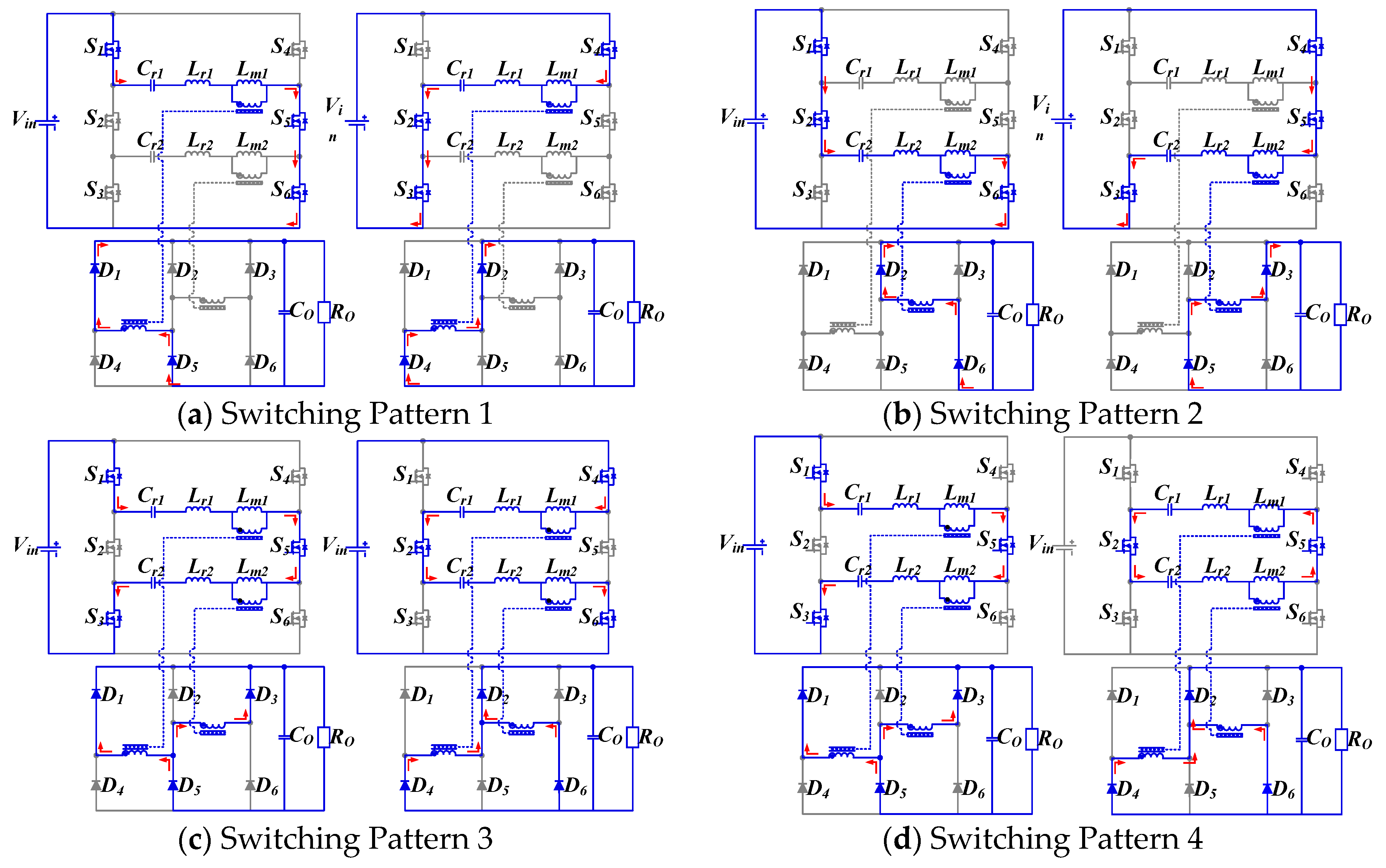
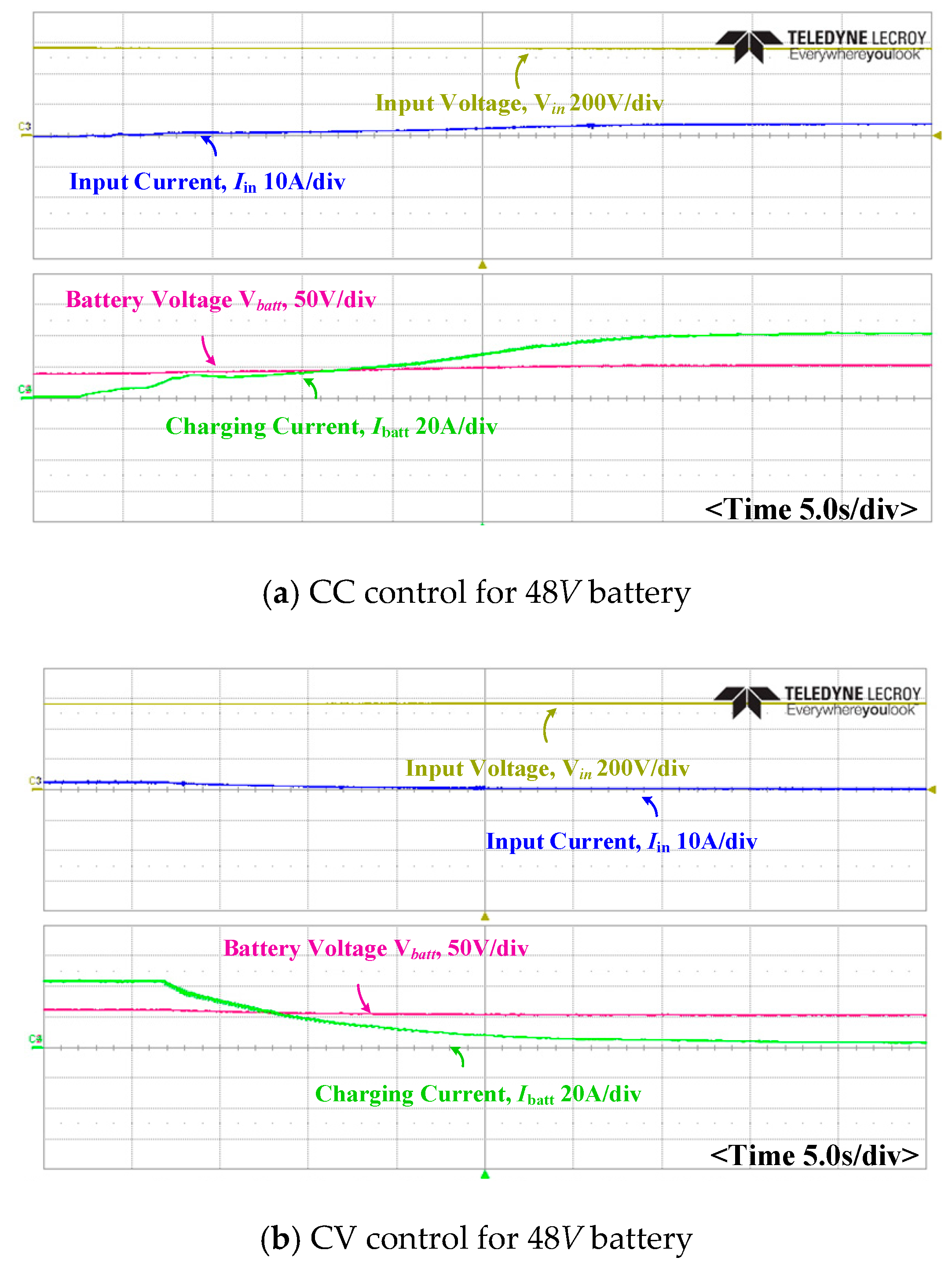
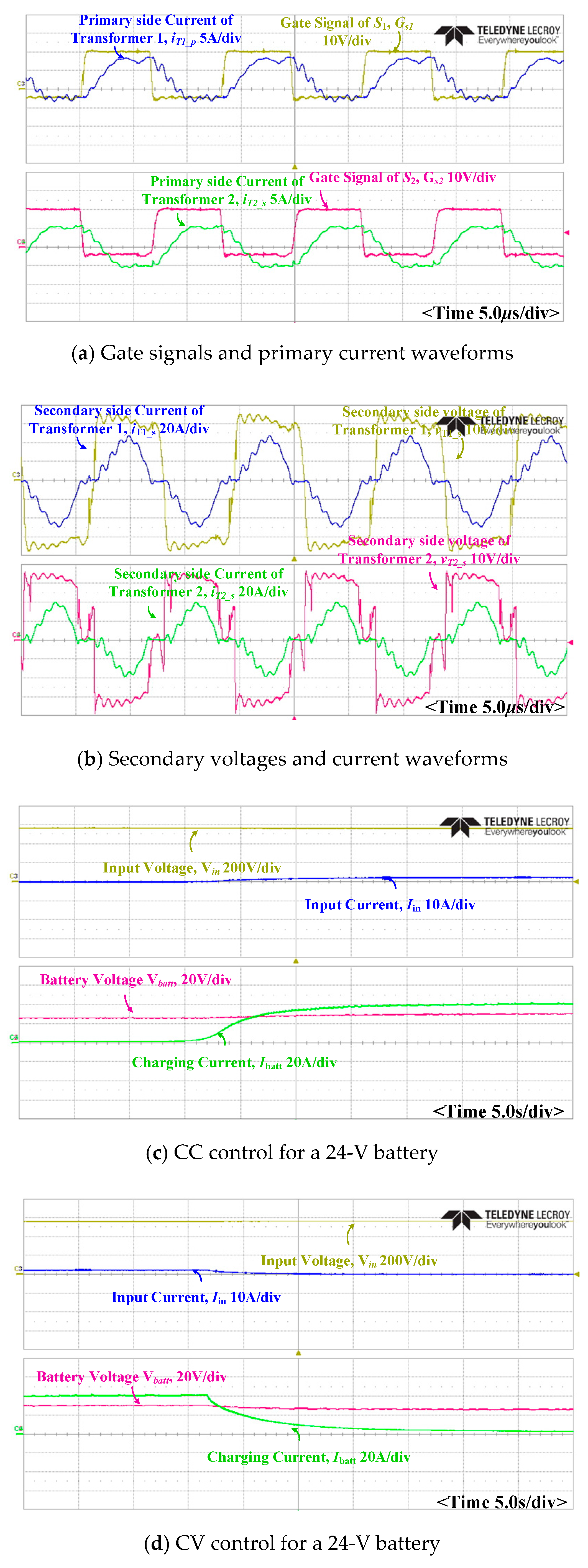
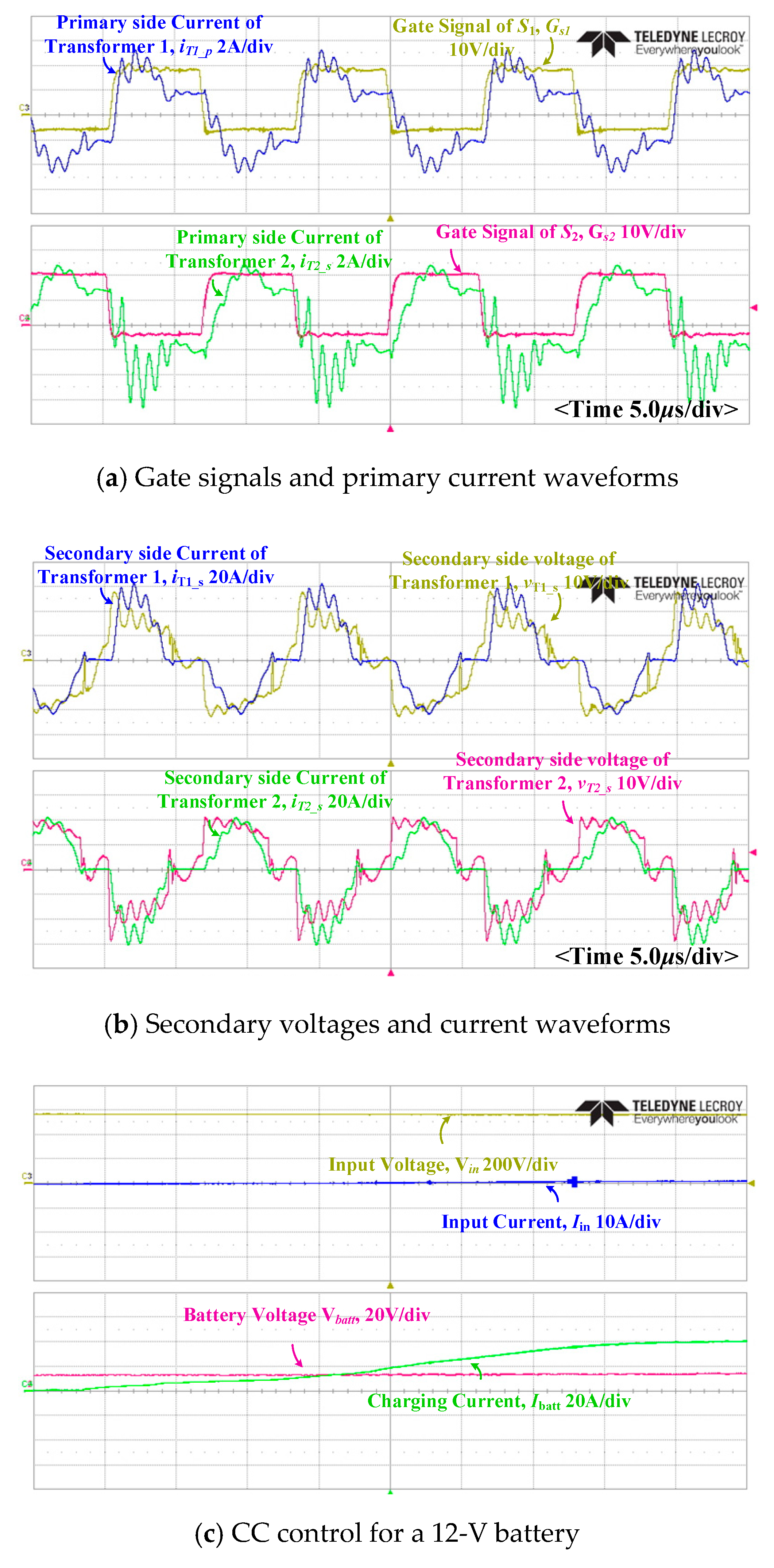
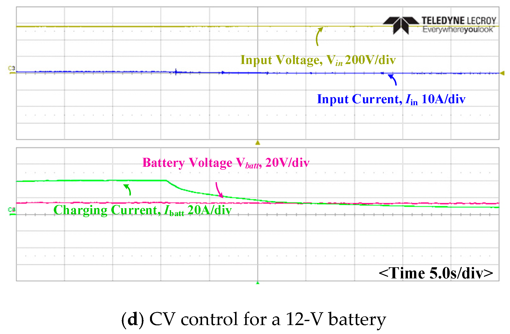
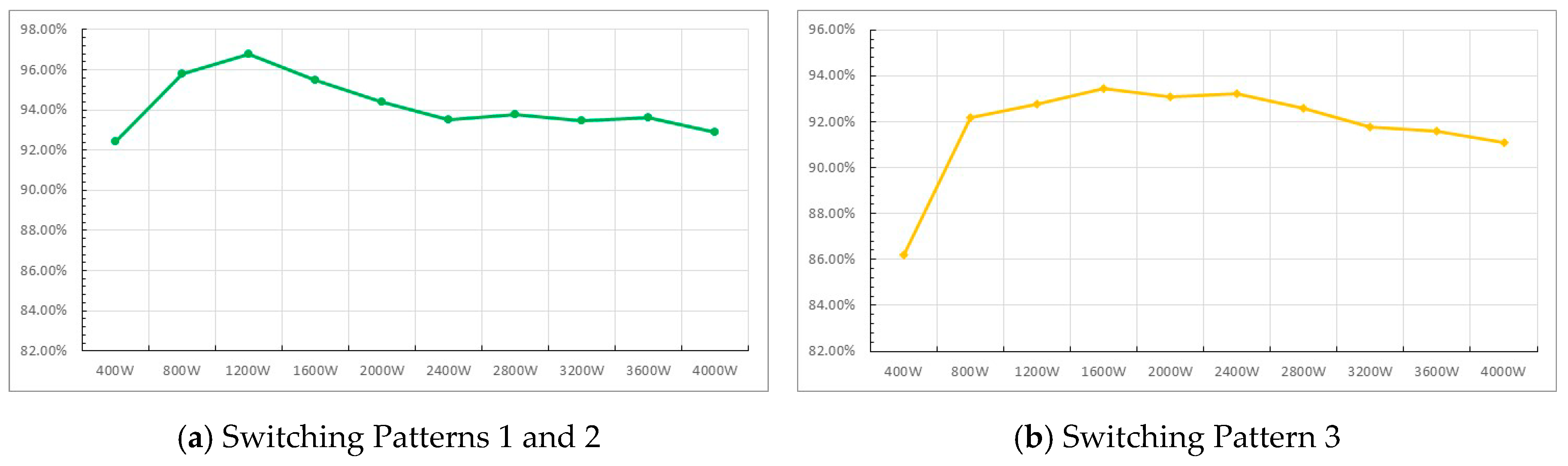
This paper introduces five different switching patterns of DI-LRC for a wide range of output voltages. Switching Patterns 1 and 2 only use one resonant tank in the DI-LRC to obtain the same voltage gain curve as the conventional single full-bridge LLC resonant converter. In Switching Pattern 3, the voltage gain is 0.5-times the nominal voltage gain of the existing LLC resonant converter, since DI-LRC is operated as a full-bridge connecting the two LLC resonant tanks in series. In Switching Pattern 4, two resonant tanks are connected in series in a manner identical to Switching Pattern 3, but they have a voltage gain of 0.25-times the nominal voltage gain, because of the half-bridge operation. In contrast to Switching Patterns 3 and 4, Switching Pattern 5 has the highest voltage gain at twice the nominal voltage, because it performs a full-bridge operation that connects the two LLC resonators in parallel. Detailed mode analysis according to each switching pattern is as follows.

2.2.1. Switching Patterns 1 and 2: Single Full-Bridge Operation

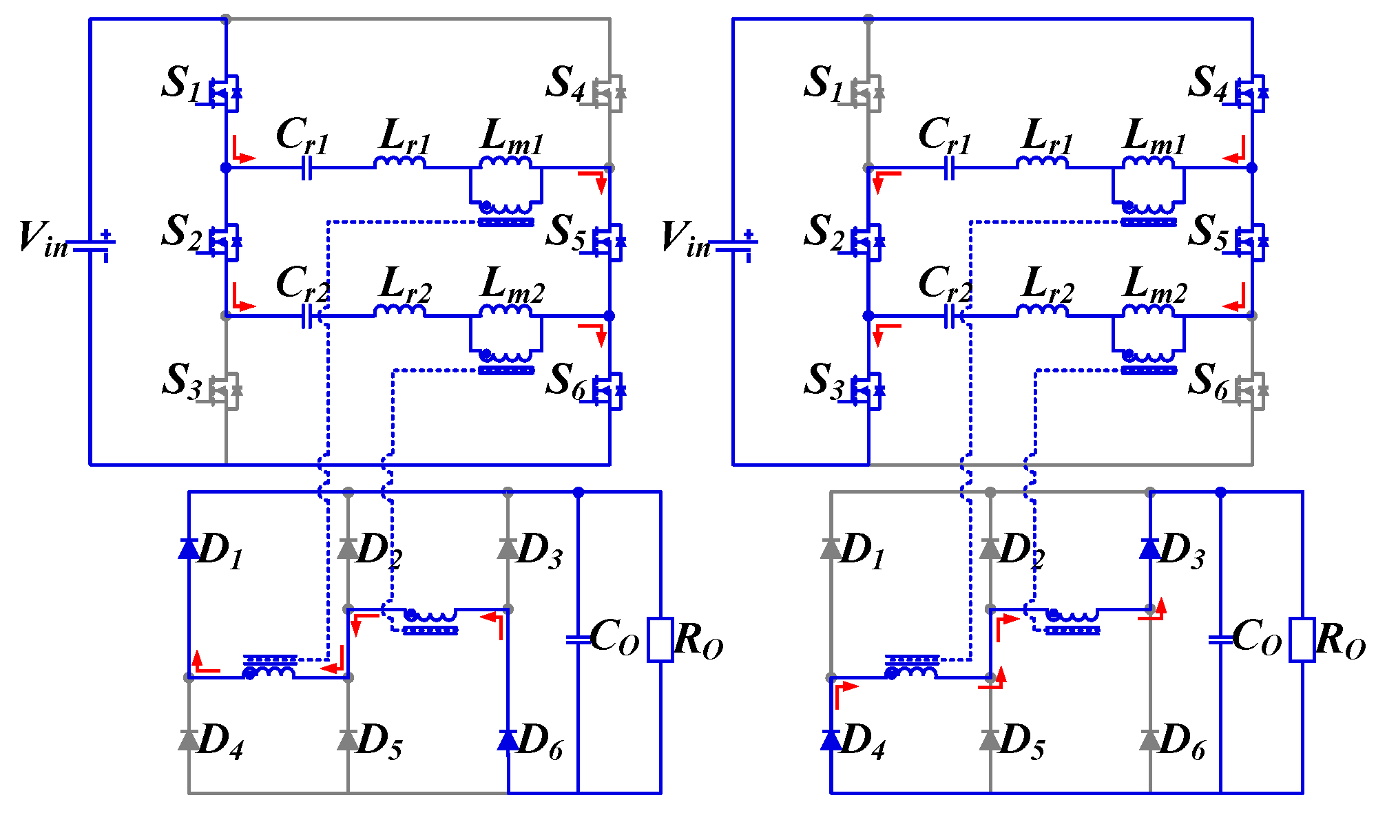
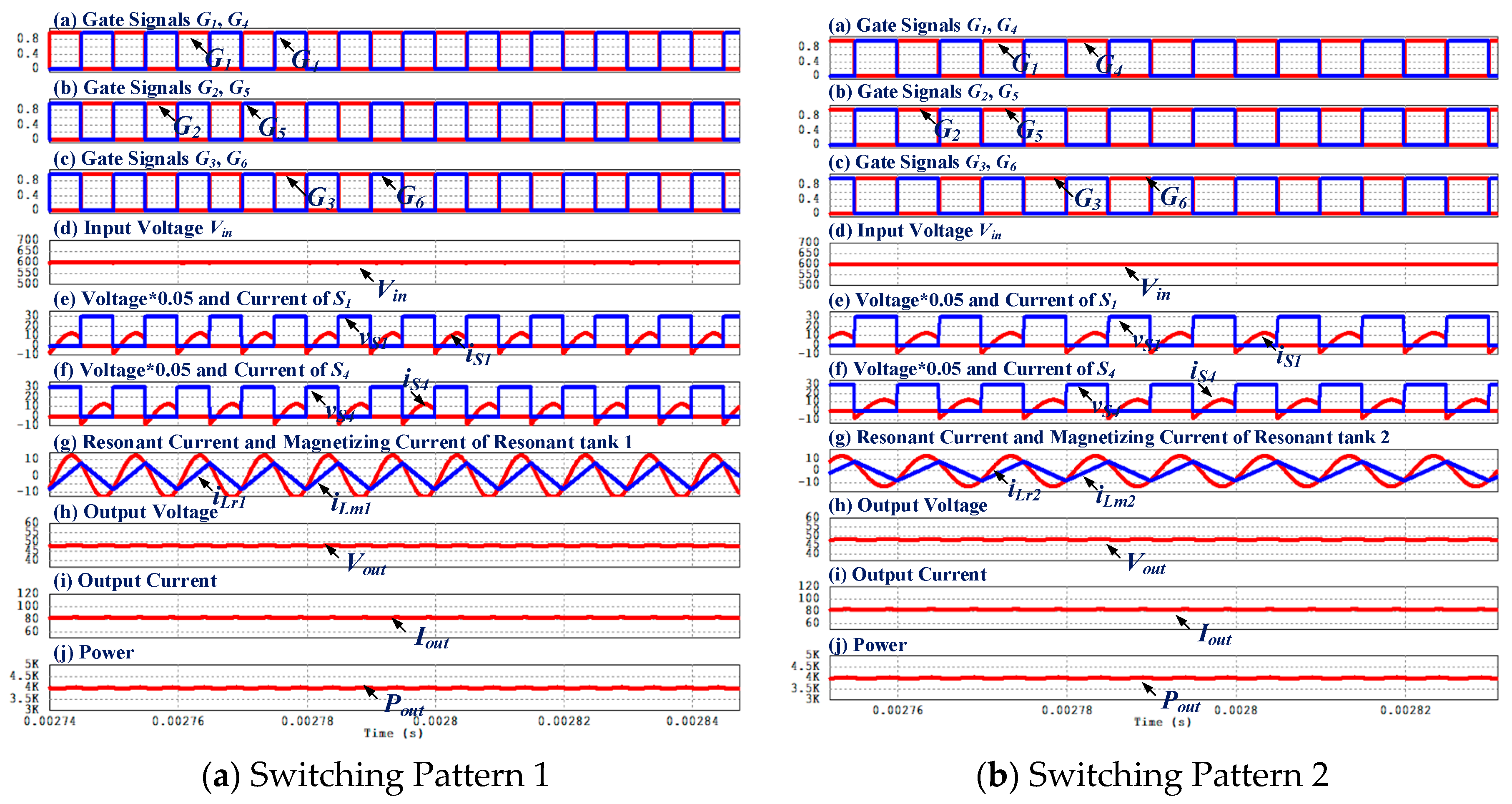
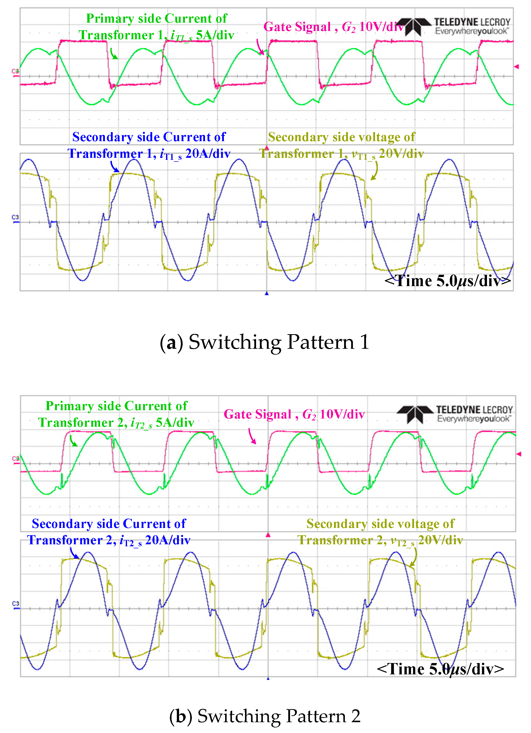
Switching Patterns 1 and 2 perform the same operation as conventional single full-bridge LLC converters, using only the resonance tanks of one of the two LLC resonance tanks, as shown in Figure 2a,b. In Switching Pattern 1, switches S1, S5, and S6 and switches S2, S3, and S4 operate complementarily at a 0.5 duty ratio to only operate the top full-bridge LLC converter. Conversely, in Switching Pattern 2, switches S1, S2, and S6 and switches S3, S4, and S5 are operated complementarily to only operate the bottom full-bridge LLC converter. Therefore, Switching Patterns 1 and 2 operate on the same principle, so this paper omits any analysis of the operation of Switching Pattern 2.
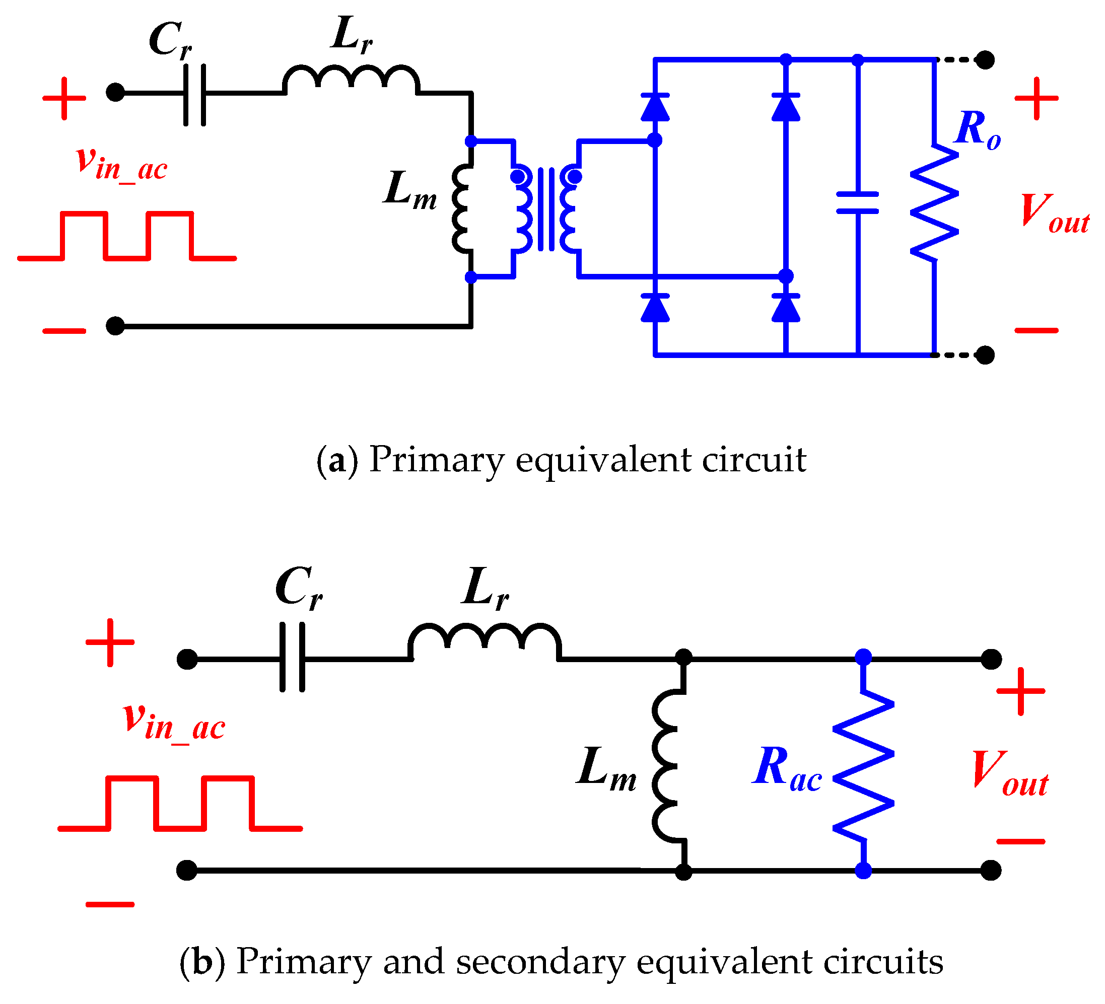
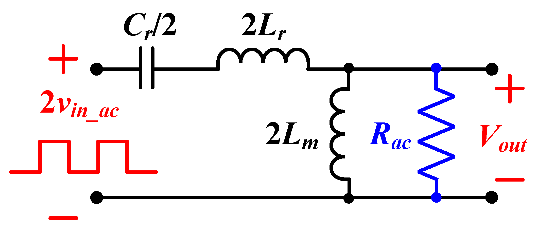
For Switching Pattern 1, +Vin is applied to the upper LLC resonance tank when switches S1, S5, and S6 are turned on, while −Vin is applied when switches S2, S3, and S4 are turned on. Thus, for the DI-LRC operating with Switching Pattern 1, it can be expressed as an equivalent circuit with a square wave input voltage of Vin, as shown in Figure 3, and the input square wave vin_ac can be represented using Fourier transform as follows.
v i n _ a c = 4 π V i n n = 1 , 3 , 5 sin ( n ω t )
The response characteristics by the switching frequency of the LLC resonant tank affect only the fundamental components of vin_ac, and the fundamental component vin_acF is expressed as follows:
v i n _ a c F = 4 π V i n sin ( ω t )
The current flowing into the resonant tank is determined by the fundamental component vin_acF of the input voltage and the characteristic impedance and can be expressed as follows:
i r ( t ) = I r , p e a k sin ( ω t φ r )
where Ir,peak is the peak value of resonant current and φ r represents the phase delay component of resonant current. Meanwhile, since the input current iin has the same waveform as the resonant current ir before the half-cycle based on the switching half-cycle, the mean value of the input current iin can be calculated by integrating the resonant current during the switching half-cycle, as follows:
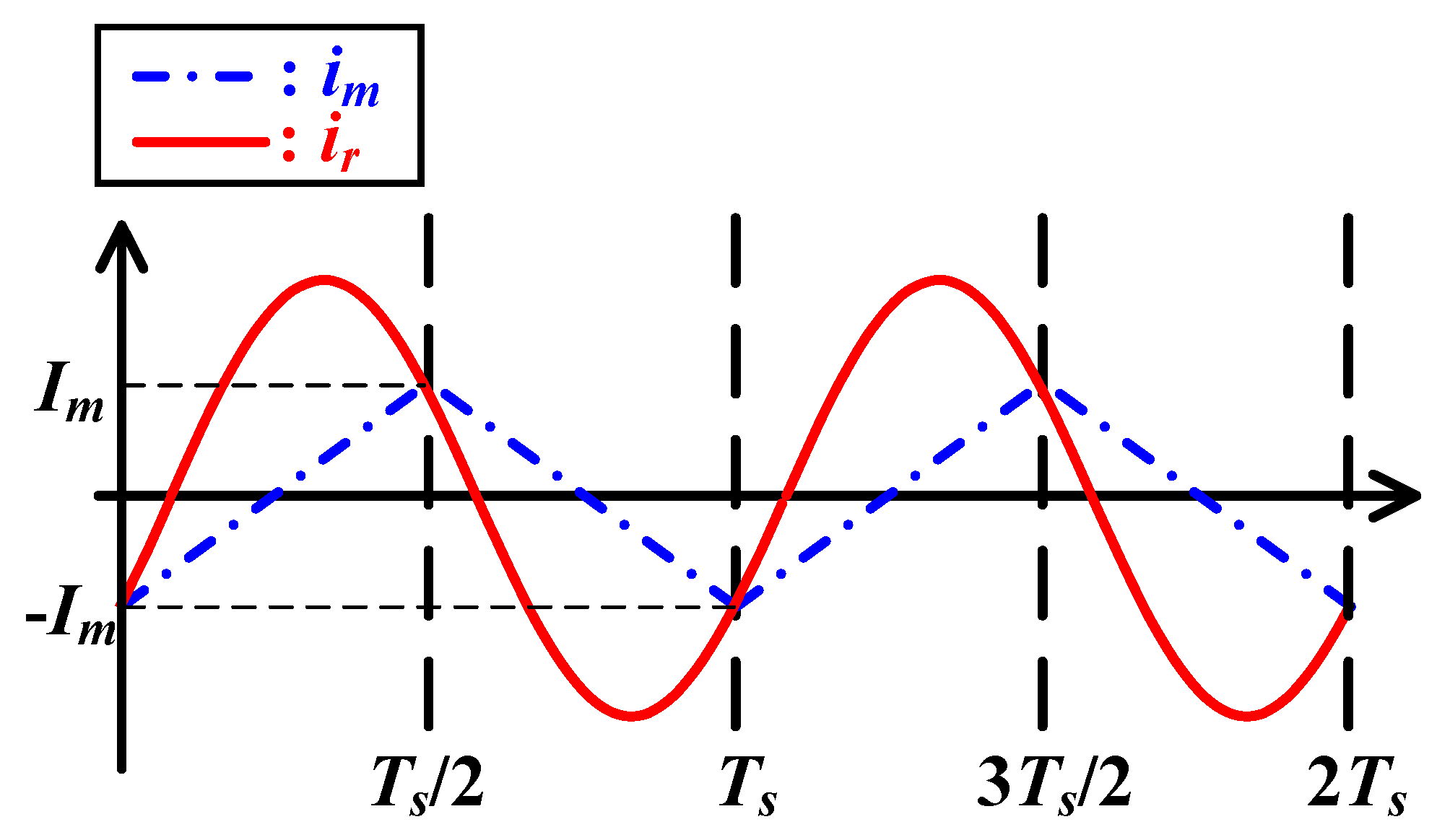
i i n ( t ) = 2 T s 0 T s / 2 i r ( t ) d t = 2 π I r , p e a k cos φ r
As shown in Figure 4, an LLC resonant converter has a resonant current of a complete sine wave when the switching frequency and resonant frequency are the same, with magnetizing current having a triangular waveform. In (3), the peak value of resonant current is replaced by the RMS value as follows:
i r ( t ) = 2 I r , r m s sin ( ω t φ r )
For the current flowing through the magnetizing inductor, the switching half-cycle is subjected to a positive voltage, and the negative voltage is applied for the remainder of the half-cycle, which can be expressed as follows:
i m ( t ) = { I m + n V o L m t , i f   0 t < T s 2 I m n V o L m ( t T s 2 ) , i f   T s 2 t < T s
where the peak value of magnetized inductor current Im must be continuous when t is Ts/2 at (6), so it can be obtained as follows:
I m = n V o T s 4 L m
In practice, since the current supplied to the load is the current that passes from the primary to the secondary side of the transformer, the relationship (8) can be obtained based on the mean of the difference between the magnetizing current im and the resonant current ir.
In addition, since the resonant and magnetizing currents have the same value in times Ts/2 and Ts, they have the same relationship, as shown in (9).
1 T s / 2 0 T / 2 [ 2 I r , r m s sin ( ω t φ r ) + n V o T s 4 L m n V o L m t ] d t = V o n R o
2 I r , r m s sin ( φ r ) = n V o T s 4 L m
Using (8) and (9), the effective value Ir,rms of resonant current can be obtained as follows:
I r , r m s = V o 4 π 2 + n 4 R o 2 T s 2 L m 2 4 2 n R o
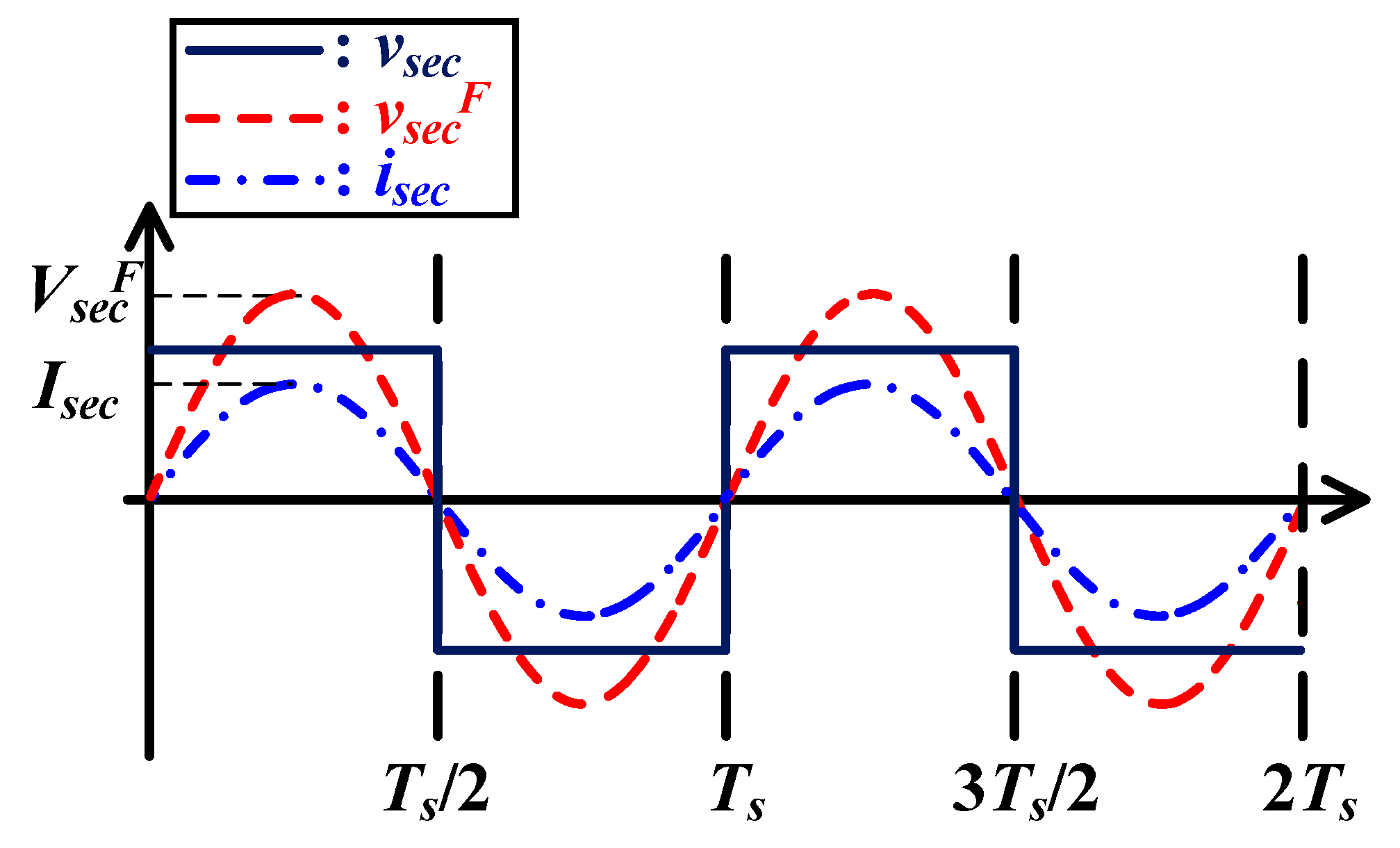
When the LLC resonant converter operates at resonant frequencies, the voltage and current waveforms flowing to the secondary side of the transformer are as shown in Figure 5 and can be obtained using Fourier series in the same way as on the primary side. The voltage and current peak values on the secondary side of the transformer are as shown in (11) and (12), respectively.
v sec ( t ) = V sec F n = 1 . 3 . 5 1 n sin ( n ω t ) = 4 π V o n = 1 . 3 . 5 1 n sin ( n ω t )
I sec = 6 V o 12 π 4 + 5 π 2 48 L m 2 n 4 R o 2 T s 2 24 π R o
When the output current is obtained using the secondary current as (13), the rectifier section and load shown in Figure 3a can be modelled as shown in (14), using the secondary voltage and current of the transformer.
I O = 2 T s 0 T s / 2 I s e c | sin ω t | d t = 2 π I s e c
R A C = V sec I sec = 8 π 2 R o
The final equivalent circuit of the DI-LRC, operated by Switching Patterns 1 and 2 through circuit interpretation for the resonant tanks and rectifier section as shown above, can be represented as shown in Figure 3b; where voltage gain M can be represented by the ratio of input voltage to output voltage, quality factor Q, the ratio of the magnetizing inductor to the return inductor m, and normalized switching frequency Fx.
M ( Q , m , F x ) = | V o u t v i n _ a c | = F x 2 m ( ( m + 1 ) F x 2 1 ) 2 + F x 2 ( F x 2 1 ) 2 m 2 Q 2
where Q = L r / C r R a c , m = L m L r , R a c = 8 π 2 N P 2 N s 2 R o , f r = 1 2 π L r C r , F x = f s f r

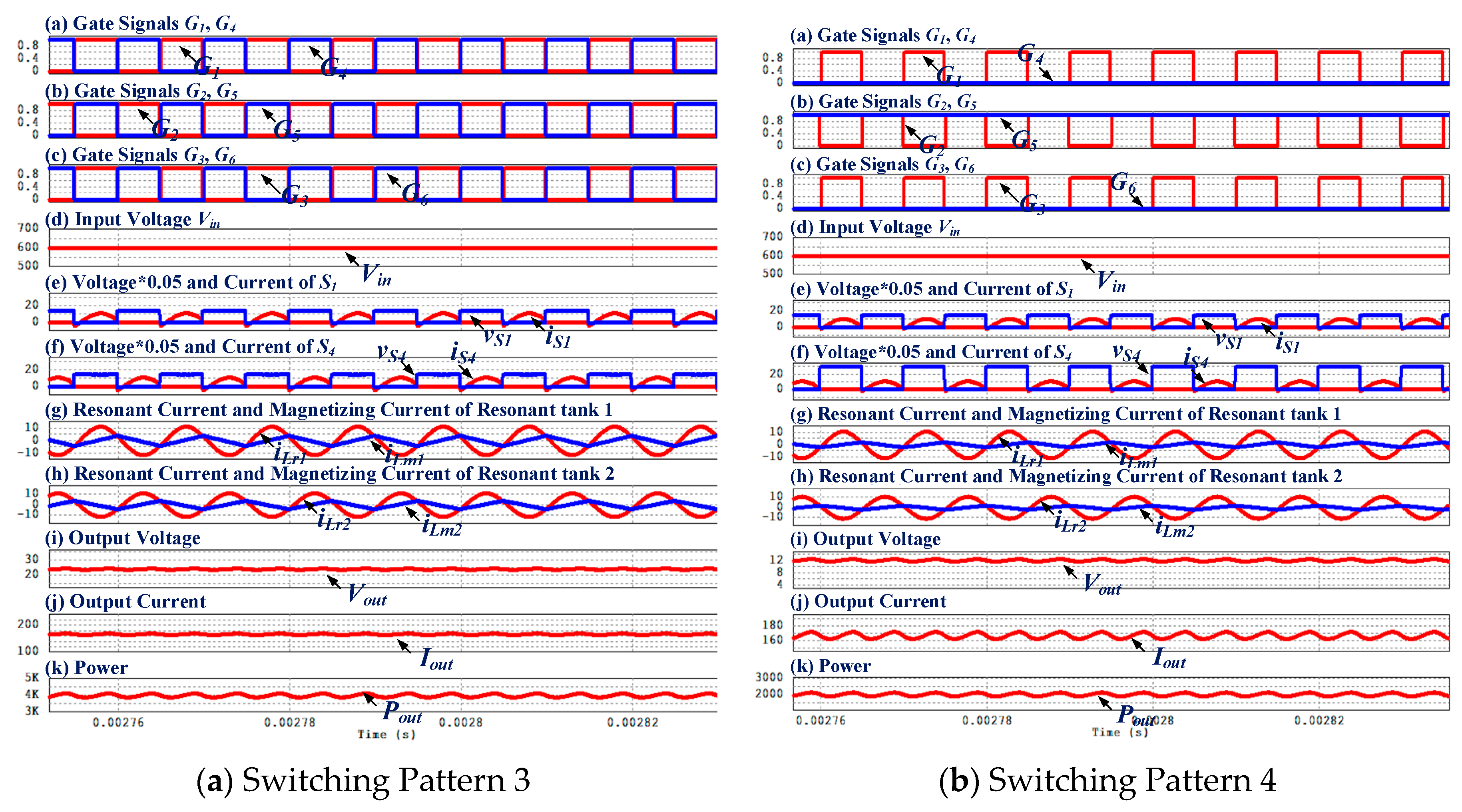
2.2.2. Switching Patterns 3: Series Full-Bridge Operation

The current pass of the DI-LRC operating with Switching Pattern 3 is shown in Figure 2c. Switches S1, S3, and S5 and switches S2, S4, and S6 are operated complementarily at a 0.5 duty ratio, so that two resonant tanks are connected in series to perform full-bridge operation. Therefore, input voltage is applied to each LLC resonant tank by half. In contrast, at the output side of the DI-LRC, three diodes turn on and have a parallel structure. Therefore, Switching Pattern 3 has an input-serial, output-parallel structure, and the equivalent circuit for detailed analysis and for calculating voltage gain is presented in Figure 6.
As shown in Figure 6, in an equivalent circuit, due to the series connection of two LLC resonance tanks, the sizes of the magnetized inductor and resonant inductor are reduced by half, the resonant capacitors have doubled, and the input voltage of Vin/2 is applied. Calculating the quality factor Qsp3 and the voltage gain using the resonance components value of the equivalent resonance tank can be achieved using (16) and (17), respectively.
Q s p 3 = ( 1 2 L r ) / ( 2 C r ) R a c = 1 2 L r / C r R a c = 1 2 Q
M s p 3 = F x 2 m 2 { ( ( m + 1 ) F x 2 1 ) 2 + F x 2 ( F x 2 1 ) 2 m 2 ( 1 2 Q ) 2 }
The quality factor Qsp3 of Switching Pattern 3 is halved as compared to the quality factor Q of Switching Patterns 1 and 2, and under conditions of Fx = 1 with the same resonant frequency and switching frequency, the voltage gain is also reduced to one-half. As the voltage gain decreases by half, the resonant current and output current also decrease by half, as calculated by (18) and (19), respectively.
I r , r m s _ s p 3 = ( 1 2 ) V o 4 π 2 + n 4 R o 2 T s 2 L m 2 4 2 n R o
I s e c _ s p 3 = 3 ( 1 2 ) V O 12 π 4 + 5 π 2 48 L m 2 n 4 R O 2 T s 2 24 π R O
As a result, the output voltage and output current are halved, and the output power is eventually reduced to 1/4 as compared to Switching Patterns 1 and 2. However, it is necessary to obtain a quality factor and voltage gain under the same power condition considering that some applications require a constant output current of a certain value, such as a battery charger. In order to operate at the same power, taking into account the half-reduced voltage gain, the output current should be quadrupled; as a result, the load resistance should be reduced to 1/4 as compared to Switching Patterns 1 and 2. Therefore, the equivalent resistance Rac_sp3_cp and quality factor Qsp3_cp, considering the same power, can be expressed as follows:
R a c _ s p 3 _ c p = 8 π 2 N P 2 N s 2 ( 1 4 R o ) = 1 4 R a c
Q s p 3 _ c p = 1 2 L r / C r R a c _ s p 3 _ c p = 1 2 L r / C r R a c / 4 = 2 Q
In the equivalent circuit of Switching Pattern 3, the quality factor was reduced by half, but the quality factor was doubled when the same power was taken into account. Therefore, the voltage gain value was calculated again using (21) as shown in (22). At resonant frequencies, the converter has a voltage gain of one-half the size of the voltage gain of Switching Patterns 1 and 2.
M s p 3 _ c p = F x 2 m 2 { ( ( m + 1 ) F x 2 1 ) 2 + F x 2 ( F x 2 1 ) 2 m 2 ( 2 Q ) 2 }
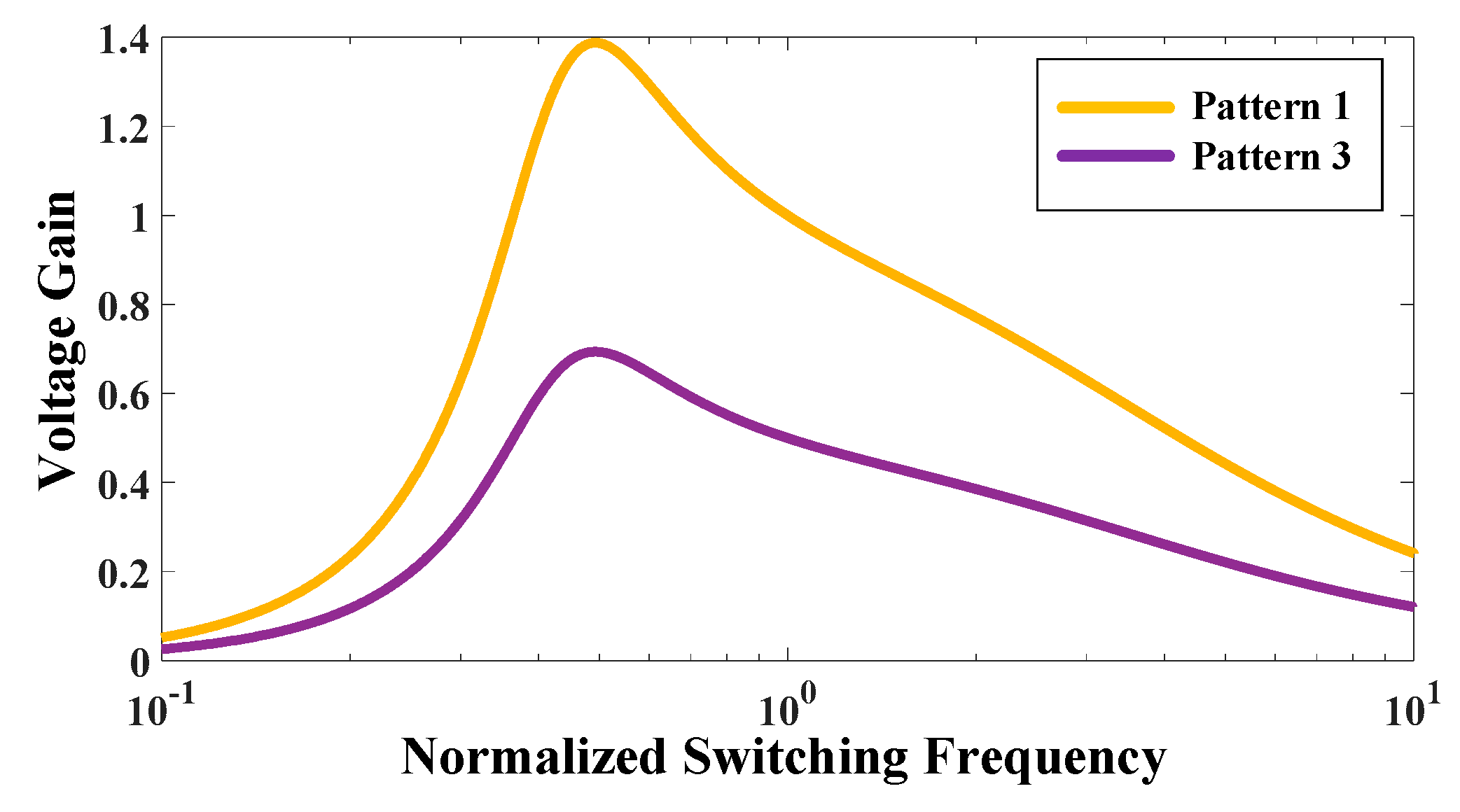
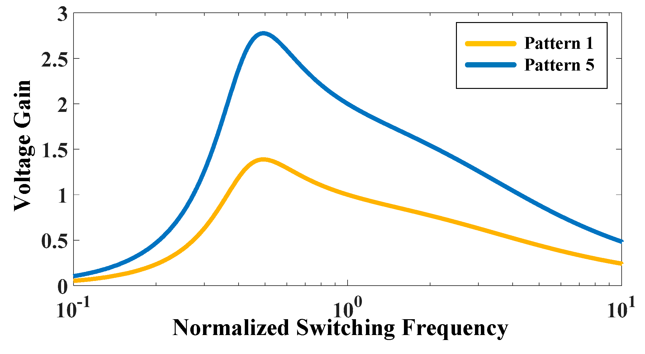
A comparison of the voltage gain curves of Switching Patterns 1 and 3 at the same power is shown in Figure 7. When m is six and the quality factor is 0.4, the maximum voltage gain for Switching Pattern 1 has a value of approximately 1.2, while that for Switching Pattern 3 is approximately 0.6.

2.2.3. Switching Patterns 4: Series Half-Bridge Operation

As shown in Figure 2d, Switching Pattern 4 connects the LLC resonant tank in series, as described previously in Switching Pattern 3; however, it always turns on switch S4 and turns on and off switches S1 and 
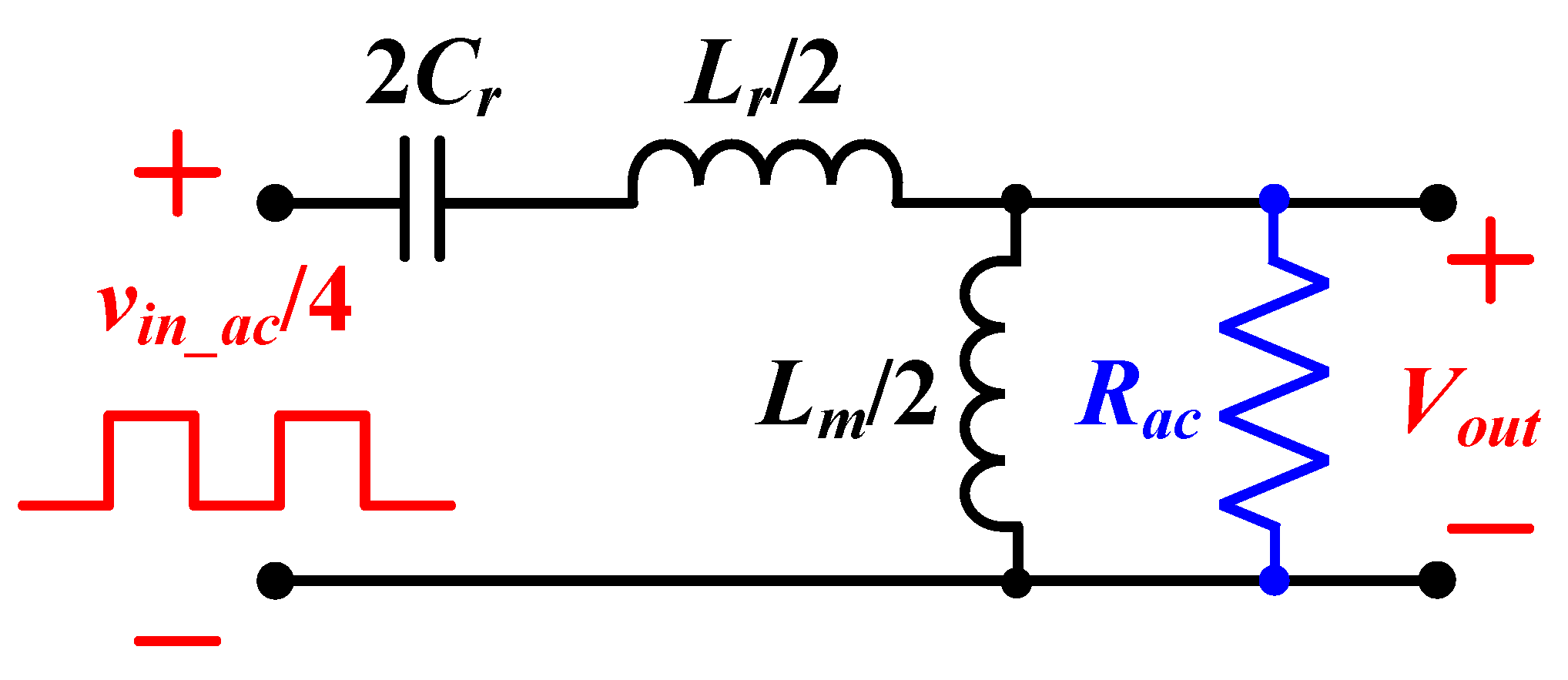
S2 complementarily as a half-bridge mode. Thus, for Switching Pattern 4, a quarter of the input voltage is applied to each resonant tank. The secondary diode rectifier has a parallel structure in which three diodes turn on, as shown in Switching Pattern 3. Therefore, DI-LRC has an input-serial output-parallel structure and can be represented as an equivalent circuit, as shown in Figure 8.
Switching Pattern 4 also requires an adjustment of the load to be analyzed based on the same power as Switching Pattern 1. Switching Pattern 4 causes the series-connected LLC resonance tank to enter half-bridge operation, so it has a 1/4 voltage gain less than Switching Pattern 1, thus reducing the output voltage and current to one quarter. As a result, the output power is reduced to 1/16. For the same power condition, the quality factor can be obtained as shown in (24) by reducing the resistance by 16 times, as shown in (23).
R a c _ s p 4 _ c p = 8 π 2 N P 2 N s 2 ( 1 16 R o ) = 1 16 R a c
Q s p 4 _ c p = 1 2 L r / C r R a c _ s p 4 = 8 Q
Under the same load condition, the quality factor in Switching Pattern 4 shows an eight-times increase over that pf Switching Pattern 1, while the voltage gain shows a one-quarter reduction in resonant frequency, as follows:
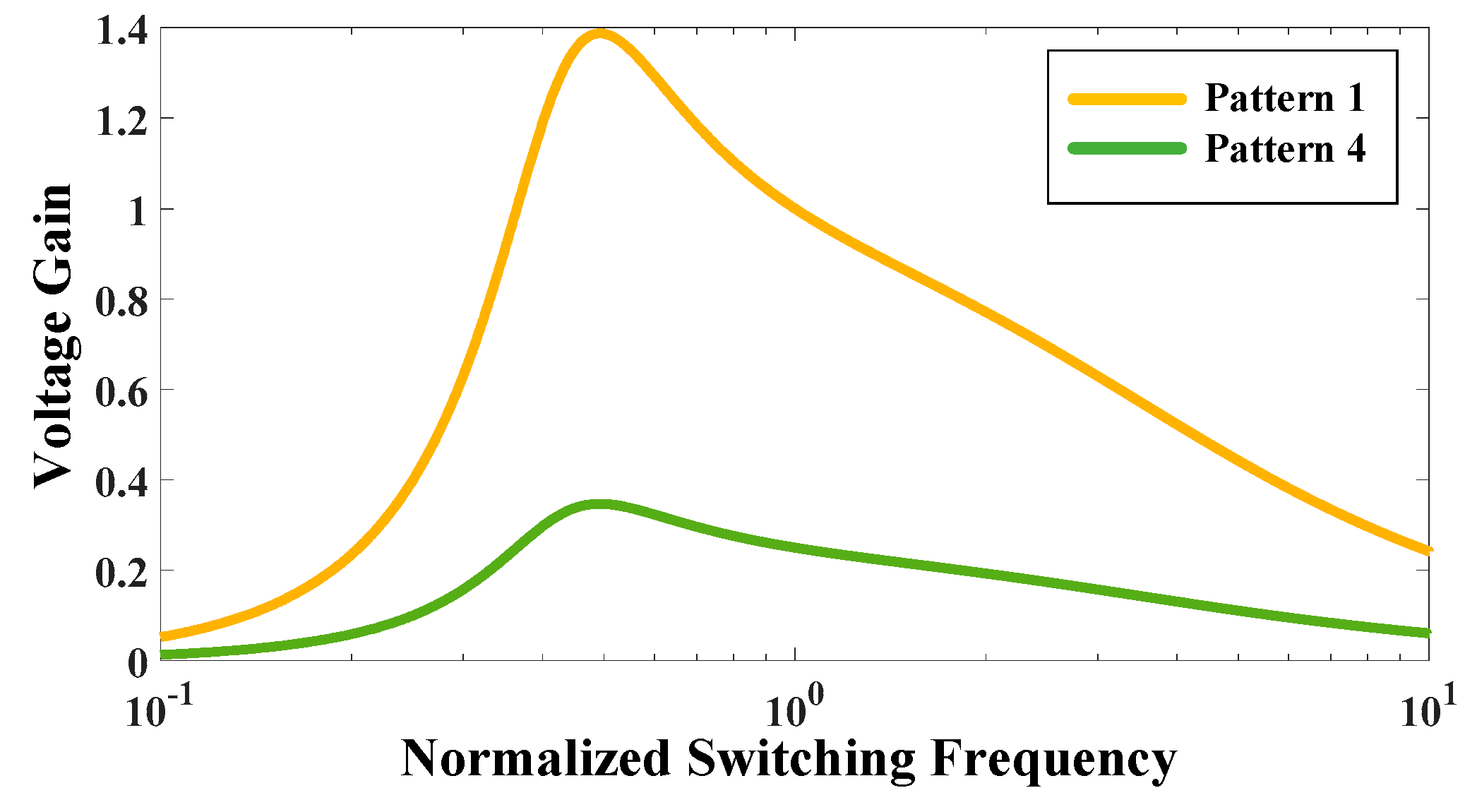
M s p 4 _ c p = F x 2 m 4 { ( ( m + 1 ) F x 2 1 ) 2 + F x 2 ( F x 2 1 ) 2 m 2 ( 8 Q ) 2 }
In Figure 9, the voltage gain curves of Switching Patterns 1 and 4 are compared when m is six and the quality factor is 0.4. In Switching Pattern 4, the voltage gain is one-quarter at the resonant frequency. The quality factor of Switching Pattern 4 has a value of 3.2 when that of Switching Pattern 1 is 0.4, so it has a curve similar to that of the voltage gain curve of the series resonant converter. However, as actual battery chargers charge the battery by fixing certain current values, the voltage gain curve in Switching Pattern 4 may have a wider voltage gain than that shown in Figure 9 when charging with an output current that is lower than 16-times the output current of Switching Pattern 1 (equal to Switching Pattern 1).

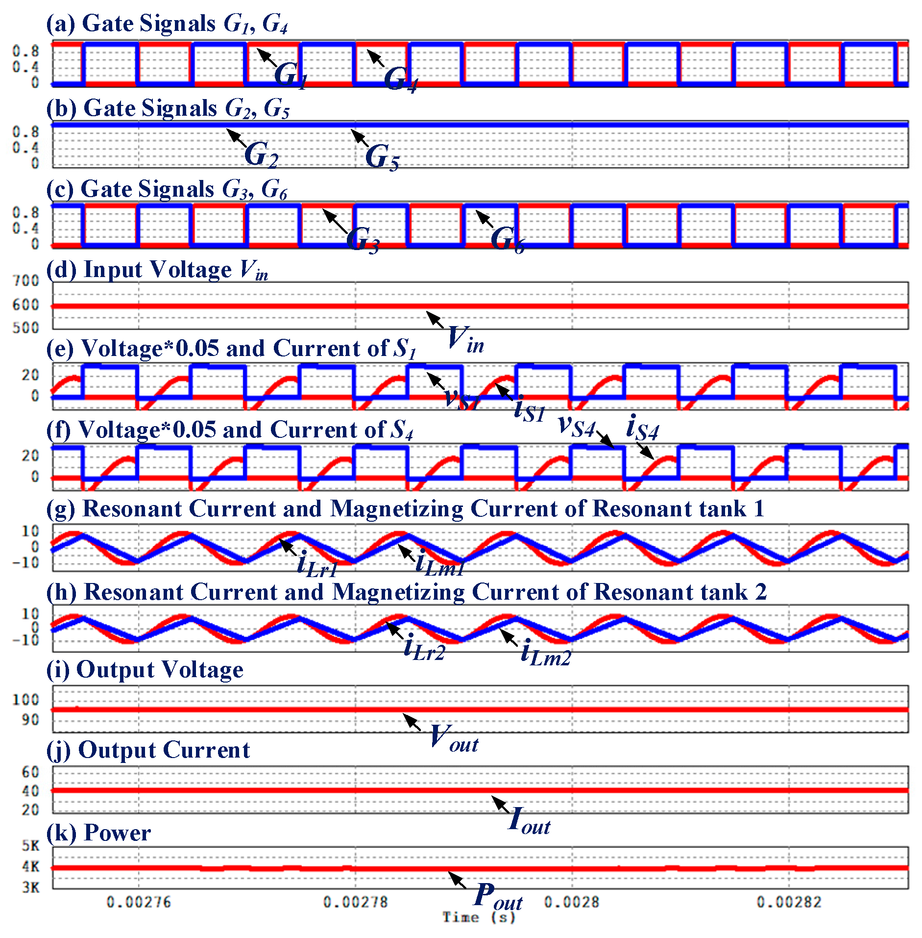
2.2.4. Switching Patterns 5: Parallel Full-Bridge Operation

The current pass for Switching Pattern 5 is shown in Figure 10. Switches S2 and S5 are always turned on, while switches S1 and S6 and switches S3 and S4 are operated complementarily in order to perform full-bridge operation connecting the two LLC resonance tanks in parallel. Therefore, each LLC resonator tank has an input-parallel structure in which an input voltage Vin is applied, and the output stage has an output serial structure in which only two diodes are turned on, making the secondary side of the transformer and the load a series connection.
In the equivalent circuit of Switching Pattern 5, as shown in Figure 11, the magnetizing inductors and resonant inductors in resonance tanks are twice the value of conventional single resonance tanks, while resonant capacitors are half the value. In addition, an equivalent resonant tank is input with twice the input voltage of a single resonant tank. Similar to Switching Patterns 3 and 4, which operate the LLC resonator tanks in series, the Q factor is obtained using the resonance components’ value of the resonant tank in Switching Pattern 5.
Q s p 5 = ( 2 L r ) / ( 1 2 C r ) R a c = 2 L r / C r R a c = 2 Q
In contrast to Switching Patterns 3 and 4, the quality factor of Switching Pattern 5 is doubled. However, for Switching Pattern 5, as shown in Figure 12, the LLC resonance tank is connected in parallel and performs a full-bridge operation, resulting in a voltage gain of twice that of the existing single LLC full-bridge operation. This results in a four-times increase in power over a single LLC full-bridge operation with twice the output voltage and output current. The load adjustment is required to be analyzed under the same power condition as the previous switching pattern analysis.
In Switching Pattern 5, load resistance Rac_sp5_cp and quality factor Qsp5_cp are as expressed in (27) and (28), respectively, as the load must be reduced to 1/4 in order to compensate for a four-times increase in power. In addition, the voltage gain of Switching Pattern 5 obtained under the same power condition using (28) is equal to that using (29).
R a c _ s p 5 _ c p = 8 π 2 N P 2 N s 2 ( 4 R o ) = 4 R a c
Q s p 5 _ c p = ( 2 L r ) / ( 1 2 C r ) R a c _ s p 5 _ c p = 2 L r / C r 4 R a c = 1 2 Q
M s p 5 _ c p = 2 F x 2 m { ( ( m + 1 ) F x 2 1 ) 2 + F x 2 ( F x 2 1 ) 2 m 2 ( 1 2 Q ) 2 }
At resonant frequency points, it has twice the voltage gain of the existing single LLC full-bridge operation, and at points other than the resonant frequency, it has another type of voltage gain curve, because the Q factor is reduced by half. In Figure 9, the voltage gain curves of Switching Patterns 1 and 5 are compared when m is six and the quality factor has a value of 0.4. Operating the switching frequency in an area below the resonant frequency with Switching Pattern 5 can result in a higher voltage gain than twice the nominal voltage. Under conditions in which a high range of boost is required, operating with Switching Pattern 5 can satisfy the high output voltage. However, under conditions where voltage gains less than one are required, switching frequencies should be increased to 10-times the resonant frequency, so Switching Pattern 1, 2, or 3 should be operated.

3. Simulation Results

The universal battery charger, which can apply the DI-LRC converter proposed in this paper, had a wide voltage range from 12–96 V. Thus, the DI-LRC converter should operate near the resonant frequency and be able to meet the wide range of output voltages required by the universal battery charger. Since the universal battery charger had a nominal input voltage of 600 V when using a power factor correction (PFC) rectifier with three-phase 380 Vac as input, the input voltage range was 575–600 V, and the nominal output power was 4 kW, so as to accommodate a charge current of 40 A from a 96-V battery, which required the highest charging voltage. Finally, the parameters of the simulation and experiment carried out in this paper are presented in Table 1. In addition, simulations were conducted so that the batteries were charged with an output voltage corresponding to each switching pattern. For simulation purposes, the batteries used equivalent circuit models, R and C.
Figure 13 shows the simulation results of Switching Patterns 1 and 2 that charged the battery with an output voltage of 48 V. (a), (b), and (c) of each simulated waveform represent the gate waveforms G1, G4, G2, G5, and G3, G6, respectively, of the switch. For Switching Pattern 1, as shown in Figure 13a, switches S1, S5, and S6 and switches S2, S3, and S4 were switched complementarily, so the upper LLC resonant tank operated as a single full-bridge. Similarly, for Switching Pattern 2, as shown in Figure 13b, switches S1, S2, and S6 and switches S3, S4, and S5 were switched complementarily, so that the lower LLC resonant tank acted as a single full-bridge operation and had an output voltage of 48 V.
At this point, the output current charging the battery was 80 A in both switching patterns, while the output power was 4 kW.
Figure 14a shows the simulation results of Switching Pattern 3 with a half voltage gain of Switching Patterns 1 and 2. As shown in the simulation results, switches S1, S3, and S5 and switches S2, S4, and S6 were switched complementarily at a 0.5 duty ratio, and the two LLC resonance tanks were connected in series to perform full-bridge operation. As a result, the output voltage was 24 V, with a voltage gain of one-half as compared to the conventional single full-bridge operation. The charging current was 160 A while charging the battery at 4 kW, which was the same power as the previous switching pattern.
In the case of Figure 14b, S5 always turned on for one cycle, and only switches S1, S3, and S2 operated complementarily at a 0.5 duty ratio, so that the two LLC resonance tanks performed a series-connected half-bridge operation. Accordingly, it had a quarter of the voltage gain of Switching Patterns 1 and 2 and the lowest output voltage among the switching patterns at 12 V. In contrast to the other switching patterns, in Switching Pattern 4, the output voltage was very low, and a large current of more than 300 A flowed to the output stage under the same output power condition as other switching patterns. This increased the current stress and conduction loss of the secondary side components. Therefore, for Switching Pattern 4, as shown in Figure 14b, the output current was limited to 160 A and operated at 2 kW, half the existing power.
Figure 15 shows the simulation results of Switching Pattern 5, which had the highest voltage gain among any of the switching patterns. As shown in the simulation results, S2 and S5 always turned on for one cycle, and S1, S6, S3 and S4 were switched complementarily at a 0.5 duty ratio so as to perform full-bridge operation with two LLC resonance tanks in parallel. Accordingly, the DI-LRC had twice the voltage gain of Switching Patterns 1 and 2, as well as an output voltage of 96 V. The output current was about 40 A and operated with the same power as Switching Patterns 1, 2, and 3.

4. Experiment Results

In this paper, the characteristics of the voltage gain change according to the switching pattern of the proposed converter were verified through an experiment on the 4-kW Class DI-LRC prototype shown in Figure 16. The DI-LRC prototype was divided into the switching network, resonant tanks, and diode rectifiers. Because the switching network had a wide switching frequency of 80–150 kHz, the power switches, which were Microsemi Corporation’s APT40SM120J, were used to operate at the above frequency. The transformer had a turn ratio of 14:1, and the resonant inductor comprising the resonant tank was composed using the leakage inductor of the transformer. The resonant capacitor was used by connecting Icel’s film capacitor 100 nF in series to meet the design value of 50 nF. The rectifier diode used Micro Commercial Corporation’s MF300C12F2, which had a short reverse recovery time for high frequency switching. Finally, the controller used Texas Instruments’ TMS320F28335. The DI-LRC received approximately 600 V with three-phase 380 V rectified and charges batteries with 12 V, 24 V, 48 V, and 96 V using various switching patterns. The experimental parameters were the same as the simulation parameters, and the output current charging the battery was limited to 40 A, accounting for the current rating of the secondary diode, in order to perform constant current-constant voltage (CC-CV) control.
The experimental results of Switching Patterns 1 and 2 are shown in Figure 17. Figure 17a presents the gate waveform on switch S2, the current on the primary and secondary sides of the transformer, and the secondary side voltage located in the upper resonant tank when operated with Switching Pattern 1. Similarly, Figure 17b shows the gate waveform in S2, the current waveform on the primary and secondary sides of the transformer, and the secondary side voltage located in the bottom resonant tank when operated by Switching Pattern 2. Comparing the two experimental waveforms yielded that Switching Pattern 2 using the lower transformer further increased the circulation current through the top switch, leading to increased conduction loss. As a result, it is preferable to use Switching Pattern 1 using the top transformer for 48-V battery charging.
Figure 18a,b each represent the experimental results of CC control and CV control in Switching Pattern 1. In order to charge the 48-V battery, the DI-LRC started operating at approximately 190 kHz, and a CC control of 40 A was performed at a switching frequency of 100 kHz. The input current at this point was approximately 3.8 A. When the 48-V battery was charged to approximately 54 V, the results indicated that it was reliably performed with CV control under CC control.
Figure 19 shows the experimental result waveform of the DI-LRC operating with Switching Pattern 3. Figure 19a shows the gate waveforms of switches S1 and S2 and the corresponding primary side current of the transformer, while Figure 19b represents the secondary side voltage and current waveforms of the top and bottom transformers.
As compared to Switching Patterns 1 and 2, the voltage and current ripple of the two transformers was increased. This was caused by a fine parameter error between the two LLC resonant tanks, which resulted in varying impedance to the resonance tank and a difference in applied voltage; this stemmed from the difference in voltage applied to the primary side of the top and bottom transformers, with varying impedance to the resonance tank due to a fine parameter error between the two LLC resonant tanks. The energy exchange of the two resonant tanks due to this voltage difference caused ripple in voltage and current. In Switching Pattern 3, the two LLC resonant tanks were connected in series, so the current flowing to the upper and lower resonant tanks was inverted in phase. Figure 19c,d shows the CC-CV control results of a 24-V battery. The input current was about 1.5 A and charged the 24-V battery at 40 A. When the battery voltage reached approximately 28 V, CV control was performed reliably. Therefore, Switching Pattern 3 allowed the battery to be reliably charged with voltage gains that were 1/2-times smaller than those of Switching Patterns 1 and 2 operating in a single full-bridge.
Figure 20 shows the experimental results of the DI-LRC operating with Switching Pattern 4. Figure 20a shows the gate waveforms of switches S1 and S2, as well as the resonant current waveforms flowing to the top and bottom transformers. Figure 20b presents the secondary side voltage, as well as the current waveforms of the top and bottom transformers, respectively. For Switching Pattern 4, similar to Switching Pattern 3, DI-LRC operated two resonant tanks in series, resulting in fine parameter errors between the two resonant tanks. Circulating current and current ripple occurred due to the voltage difference on the secondary side of the transformer caused by parameter error. Figure 20c,d respectively represent CC control and CV control waveforms when charging a 12-V battery. For Switching Pattern 4, DI-LRC had an input current of approximately 1 A, and 12-V CC control was performed with 40 A charging current. In addition, if the battery voltage is charged above a certain voltage, a CV operation should be performed.
Figure 21 shows an experimental waveform when the DI-LRC operated in Switching Pattern 5. Figure 21a represents the gate waveform of switches S1 and S2 and the transformer current accordingly. Figure 21b represents the secondary voltage, as well as the current waveform of the upper and lower transformers. In Switching Pattern 5, because the two LLC resonance tanks operated in parallel, there was no voltage imbalance between the two resonant tanks that occurred in the series structure, thus reducing ripple phenomena. Figure 21c,d represent CC and CV control waveforms of 96-V batteries, respectively, each with an input current of approximately 7 A and an output current of 40 A.
Figure 22 shows efficiency graphs according to switching patterns and load condition. Aside from Switching Pattern 4, the efficiency was measured based on 4 kW, while the efficiency was measured by 2 kW in Switching Pattern 4. A single operating mode with Switching Pattern 1 had a maximum efficiency of about 96.5% at a 1.2-kW load condition and tended to decrease with increasing load. By contrast, Switching Pattern 3 had a maximum efficiency of about 93.5% at 40% load, while Switching Pattern 4 had a maximum efficiency of about 93.5% at 60% load. In Switching Patterns 3 and 4, in which two LLC resonant tanks were connected in series, the difference in voltage applied to the two resonant tanks resulted in a circulating current between the resonant tanks. When the DI-LRC was operated by Switching Pattern 5, a small current flowed into each LLC resonance tank, because the resonance tank was connected in parallel. This indicated that DI-LRC operated with high efficiency and had a maximum efficiency of about 96.5% for the 30% load condition.

5. Conclusions

In this paper, a novel dual integrated LLC resonant converter (DI-LRC) with two LLC resonance tanks was proposed. The proposed converter was a structure incorporating two LLC full-bridge converters. Using the five switching patterns described, it could be operated on a total of four different voltage gain curves, resulting in a wide output voltage range.
The equivalent circuits of DI-LRC were analyzed for each switching pattern, based on which the quality factor and voltage transmission ratio were calculated according to each switching pattern. In this paper, the simulation and experiment of a 4-kW battery charger were performed in order to verify the performance of the proposed DI-LRC. When the DI-LRC was operated with a switching pattern with a voltage gain of one at resonant frequencies, it had an output voltage of about 48 V and a maximum efficiency of 96.5% in the 30% load condition.
Meanwhile, Switching Patterns 3 and 4, with voltage gains of 0.5 and 0.25, respectively, at resonant frequency had output voltages of 24 V and 12 V, respectively; Switching Pattern 3 had a maximum efficiency of 93.5% at 40% load, while Switching Pattern 4 had a maximum efficiency of 93.5% at 60% load. The DI-LRC had a comparatively low efficiency by the generation of circulating currents due to the difference of impedance between two LLC resonance tanks connected in series when operated by Switching Patterns 3 and 4. In contrast, when the DI-LRC operated in Switching Pattern 5, a relatively low current flowed because the two LLC resonant tanks were connected in parallel.
As a result, the DI-LRC showed a high efficiency overall and a maximum efficiency of 96.5% at 30% load. When the DI-LRC operated with Switching Pattern 5, it had a voltage gain of two at a resonant frequency and a 96-V output voltage. Based on these results, the proposed DI-LRC was verified as suitable for the battery charger, which required high efficiency and a wide output voltage range.

Author Contributions

B.-Y.C. and S.-R.L. conceived of and designed the experiment; B.-Y.C., S.-R.L., and J.-W.K. performed the experiment; B.-Y.C. and S.-R.L. analyzed the theory. B.-Y.C., J.-W.K., and W.-S.J. wrote the manuscript. C.-Y.W. participated in research plan development and revised the manuscript. All authors have contributed to the manuscript.

Funding

This research received no external funding.

Acknowledgments

This work was supported by the National Research Foundation of Korea (NRF) grant funded by the Korea government (MSIP) (No. 2019R1A2C2007216).

Conflicts of Interest

The authors declare no conflict of interest.

References

  1. Vu, H.; Choi, W. A Novel Dual Full-Bridge LLC Resonant Converter for CC and CV Charges of Batteries for Electric Vehicles. IEEE Trans. Ind. Electron. 2018, 65, 2212–2225. [Google Scholar] [CrossRef]
  2. Wang, H.; Li, Z. A PWM LLC Type Resonant Converter Adapted to Wide Output Range in PEV Charging Applications. IEEE Trans. Power Electron. 2018, 33, 3791–3801. [Google Scholar] [CrossRef]
  3. Musavi, F.; Craciun, M.; Gautam, D.S.; Eberle, W.; Dunford, W.G. An LLC Resonant DC/DC Converter for Wide Output Voltage Range Battery Charging Applications. IEEE Trans. Power Electron. 2013, 28, 5437–5445. [Google Scholar] [CrossRef]
  4. Han, H.; Choi, Y.; Choi, S.; Kim, R. A High Efficiency LLC Resonant Converter with Wide Ranged Output Voltage Using Adaptive Turn Ratio Scheme for a Li-Ion Battery Charger. In Proceedings of the IEEE Vehicle Power and Propulsion Conference (VPPC), Hangzhou, China, 17–20 October 2016. [Google Scholar]
  5. Hua, C.; Fang, Y.; Lin, C. LLC resonant converter for electric vehicle battery chargers. IET Power Electron. 2016, 9, 2369–2376. [Google Scholar] [CrossRef]
  6. Musavi, F.; Craciun, M.; Gautam, D.S.; Eberle, W. Control Strategies for Wide Output Voltage Range LLC Resonant DC-DC Converters in Battery Chargers. IEEE Trans. Veh. Technol. 2014, 63, 1117–1125. [Google Scholar] [CrossRef]
  7. Deng, J.; Li, S.; Hu, S.; Mi, C.C.; Ma, R. Design Methodology of LLC Resonant Converters for Electric Vehicle Battery Chargers. IEEE Trans. Veh. Technol. 2014, 63, 1581–1592. [Google Scholar] [CrossRef]
  8. Hu, S.; Deng, J.; Mi, C.; Zhang, M. LLC resonant converters for PHEV battery chargers. In Proceedings of the Twenty-Eighth Annual IEEE Applied Power Electronics Conference and Exposition (APEC), Long Beach, CA, USA, 17–21 March 2013. [Google Scholar]
  9. Deng, J.; Mi, C.C.; Ma, R.; Li, S. Design of LLC Resonant Converters Based on Operation-Mode Analysis for Level Two PHEV Battery Chargers. IEEE/ASME Trans. Mechatron. 2015, 20, 1595–1606. [Google Scholar] [CrossRef]
  10. Wang, H.; Dusmez, S.; Khaligh, A. A novel approach to design EV battery chargers using SEPIC PFC stage and optimal operating point tracking technique for LLC converter. In Proceedings of the IEEE Applied Power Electronics Conference and Exposition (APEC), Fort Worth, TX, USA, 16–20 March 2014. [Google Scholar]
  11. Wang, H.; Dusmez, S.; Khaligh, A. Maximum Efficiency Point Tracking Technique for LLC-Based PEV Chargers Through Variable DC Link Control. IEEE Trans. Ind. Electron. 2014, 61, 6041–6049. [Google Scholar] [CrossRef]
  12. Sun, X.; Li, X.; Shen, Y.; Wang, B.; Guo, X. Dual-Bridge LLC Resonant Converter with Fixed-Frequency PWM Control for Wide Input Applications. IEEE Trans. Power Electron. 2017, 32, 69–80. [Google Scholar] [CrossRef]
  13. Wu, H.; Zhan, X.; Xing, Y. Interleaved LLC Resonant Converter with Hybrid Rectifier and Variable-Frequency Plus Phase-Shift Control for Wide Output Voltage Range Applications. IEEE Trans. Power Electron. 2017, 32, 4246–4257. [Google Scholar] [CrossRef]
  14. Wu, H.; Li, Y.; Xing, Y. LLC Resonant Converter with Semiactive Variable-Structure Rectifier (SA-VSR) for Wide Output Voltage Range Application. IEEE Trans. Power Electron. 2016, 31, 3389–3394. [Google Scholar] [CrossRef]
Figure 1. The dual integrated LLC resonant converter circuit.
Electronics 08 00759 g001
Figure 2. The current paths depending on the switching patterns (Patterns 1~4).
Electronics 08 00759 g002
Figure 3. Equivalent circuit for Switching Pattern 1.
Electronics 08 00759 g003
Figure 4. Resonant and magnetizing current waveforms at the resonant frequency.
Electronics 08 00759 g004
Figure 5. Voltage and current waveforms at the secondary side.
Electronics 08 00759 g005
Figure 6. Equivalent circuit of Switching Pattern 3.
Electronics 08 00759 g006
Figure 7. Voltage gain curves of Switching Patterns 1 and 3.
Electronics 08 00759 g007
Figure 8. Equivalent circuit of Switching Pattern 4.
Electronics 08 00759 g008
Figure 9. Voltage gain curves of Switching Patterns 1 and 4.
Electronics 08 00759 g009
Figure 10. Current path of Switching Pattern 5.
Electronics 08 00759 g010
Figure 11. Equivalent circuit of Switching Pattern 5.
Electronics 08 00759 g011
Figure 12. Voltage gain curves of Switching Patterns 1 and 5.
Electronics 08 00759 g012
Figure 13. Simulation waveforms of Switching Patterns 1 and 2.
Electronics 08 00759 g013
Figure 14. Simulation waveforms of Switching Patterns 3 and 4.
Electronics 08 00759 g014
Figure 15. Simulation waveforms of Switching Pattern 5.
Electronics 08 00759 g015
Figure 16. Configuration of the experiment system.
Electronics 08 00759 g016
Figure 17. Experimental results of Switching Patterns 1 and 2.
Electronics 08 00759 g017
Figure 18. CC-CV control experimental results of Switching Pattern 1.
Electronics 08 00759 g018
Figure 19. Experimental results of Switching Pattern 3.
Electronics 08 00759 g019
Figure 20. Experimental results of Switching Pattern 4.
Electronics 08 00759 g020aElectronics 08 00759 g020b
Figure 21. Experimental results of Switching Pattern 5.
Electronics 08 00759 g021aElectronics 08 00759 g021b
Figure 22. Efficiency depending on the switching patterns.
Electronics 08 00759 g022aElectronics 08 00759 g022b
Table 1. Simulation parameters.
ParameterValueUnitParameterValueUnit
Input Voltage Range575~600VTurn Ratio14
Maximum Rated Power4kWPrimary Turns39turns
Resonant Frequency100kHzMagnetizing Inductance197μH
Quality Factor0.167Inductance Ratio (m)4.94
Resonant Capacitor50nFDead Time150ns
Resonant Inductance50μHSwitch Output Capacitance115pF

