Article

Analysis and Design of a ZVT Resonant Boost Converter Using an Auxiliary Resonant Circuit

Department of Electrical and Computer Engineering, Sungkyunkwan University, Suwon 16419, Korea
*
Author to whom correspondence should be addressed.
Electronics 2019, 8(4), 466; https://doi.org/10.3390/electronics8040466
Submission received: 2 April 2019 / Revised: 14 April 2019 / Accepted: 22 April 2019 / Published: 25 April 2019
(This article belongs to the Special Issue Advanced Power Conversion Technologies)

Abstract

:
In this paper, a new zero voltage transition (ZVT) resonant boost converter is proposed. A typical boost converter generates switching losses at turning on and turning off, and these losses cause a reduction in the efficiency of the whole system. This proposed ZVT resonant boost converter utilizes a soft switching method, using an auxiliary circuit with a resonant inductor, capacitor, and two auxiliary switches. Therefore, it can reduce switching losses more so than the conventional hard switching converter. Also, the conduction period of the resonant inductor current is reduced by using a modified circuit. An experiment is conducted with the converter, which steps up the voltage from 200 V to 380 V and its switching frequency and output power are 30 kHz and 4 kW, respectively. It is confirmed that the experimental results and simulation results are the same and the validity of this proposed converter is verified. The conventional converter and proposed converter are analyzed by comparing the experimental results of two converters under the same conditions. It is confirmed that all switches can achieve soft switching and the proposed converter improves on the conventional converter by measuring the efficiency of two converters.

1. Introduction

There has been an increase in the interest of using renewable energy sources to replace fossil fuels in order to resolve problems related to environmental destruction and to combat climate change and extreme weather trends that may be caused by environmental and air pollution that have resulted from recent rapid industrialization [1,2].
Various potential sources of alternate energy, including solar, wind, tidal, and hydrogen energy, have been the subject of intensive research. One of the disadvantages of using fuel cells and photovoltaic solar cells is that they have very low efficiency. Thus, it is very important to improve the efficiency of power conversion systems. As a result, much research has been undertaken to improve the efficiency of DC–DC converters [3,4,5].
A high switching frequency is required in the design of DC–DC converters that have a compact [6,7,8]. Non-ideal switching elements in hard switching converters cause switching losses because voltage and current are superimposed during switching and the higher the switching frequency, the greater the switching losses. These losses can be reduced through the use of soft switching. Many research papers on soft-switched resonant DC–DC converters with zero voltage switching (ZVS) and zero current switching (ZCS) techniques have been published, and several techniques that reduce switching losses have been proposed [9,10]. A Zero Current Transition (ZCT) converter can achieve ZCS using an auxiliary circuit, where the resonance conditions are not affected by variations in the load [11]. But the switching losses occur during the ZCT turn-off by the reverse recovery current. The current stress of the main switch and the conduction losses increase, since part of the current through the resonant inductor flow through the main switch. A zero voltage transition (ZVT) converter has an advantage where ZVS and ZCS can be achieved for a wide load range by using an auxiliary circuit [12,13,14].
A ZVT converter is used with a resonant inductor and capacitor to satisfy the ZVT condition. A resonant inductor through current is a reactive current because the resonance energy does not have a significant effect on the output and a resonant inductor is high current because the resonant current and the reactive current are the same. Thus, a highly resonant current increases losses of passive and active devices and the overall system efficiency is reduced.
In a conventional converter, the resonant inductor current flows continuously through the auxiliary circuit. Thus, the proposed ZVT Boost converter has a modified resonant circuit to reduce conduction loss.
This paper proposes a resonant ZVT boost DC–DC converter that uses an auxiliary resonant circuit to reduce switching losses and to improve converter efficiency. The resonant circuit is composed of a resonant inductor, a resonant capacitor, and an auxiliary switch. The auxiliary circuit is used in this converter to implement a soft-switching method. The switch of the auxiliary circuit also performs a soft-switching method through the resonant circuit. Furthermore, the conduction period of the resonant inductor is reduced using a modified circuit. And this leads to a reduction in the switching losses and an improvement in the overall system efficiency, as compared to a conventional converter at the same frequency.

2. Resonant Boost DC–DC Converter

2.1. ZVT Resonant Boost Converter

Figure 1a shows a conventional resonant ZVT boost converter. Its auxiliary circuit is composed of a boost converter, an auxiliary switch, a resonant inductor, two resonant capacitors, and two diodes. The resonant capacitor is discharged before the current flows through the body diode. These resonant components make a partial resonant path for the main switch to perform soft switching under the ZVT, using the resonant circuit [15]. However, the freewheeling period of the resonant inductor current causes a conduction loss of the diode and resonant inductor. This causes a reduction in the whole system’s efficiency.
Figure 1b shows the proposed resonant ZVT boost converter. The converter is composed of a boost converter, a main inductor, two auxiliary switches, a resonant capacitor, and an auxiliary circuit with an auxiliary capacitor. The conduction period of the resonant inductor is reduced, using a modified circuit. And this leads to a reduction in the switching losses and an improvement in the overall system efficiency.
Figure 2 shows each waveform of the resonant inductor voltage and current for the conventional and proposed converter. The current conduction period of the proposed converter shown in Figure 2b is shorter than the conventional converter shown in Figure 2a.

2.2. Analysis of Proposed Converter

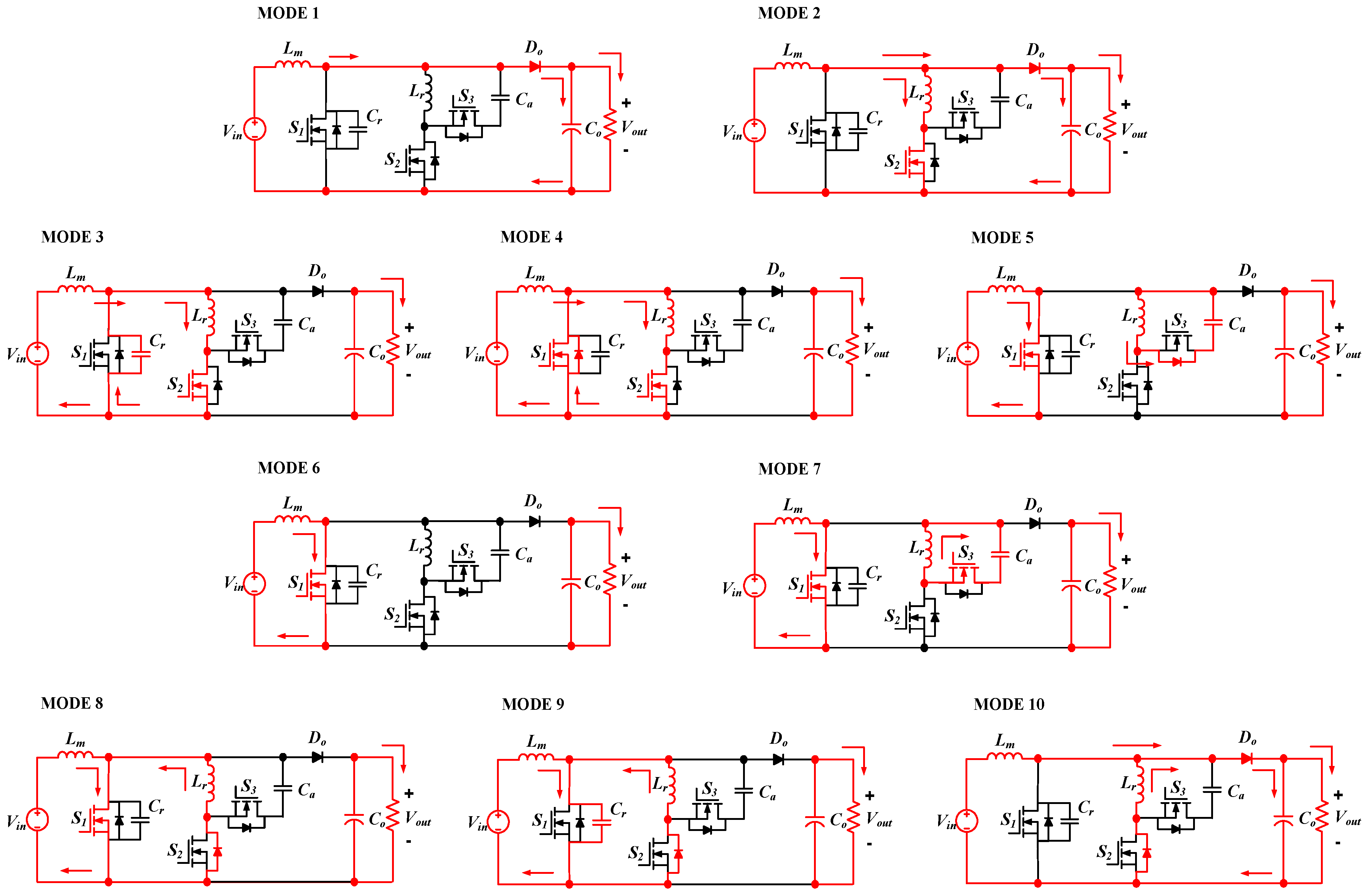
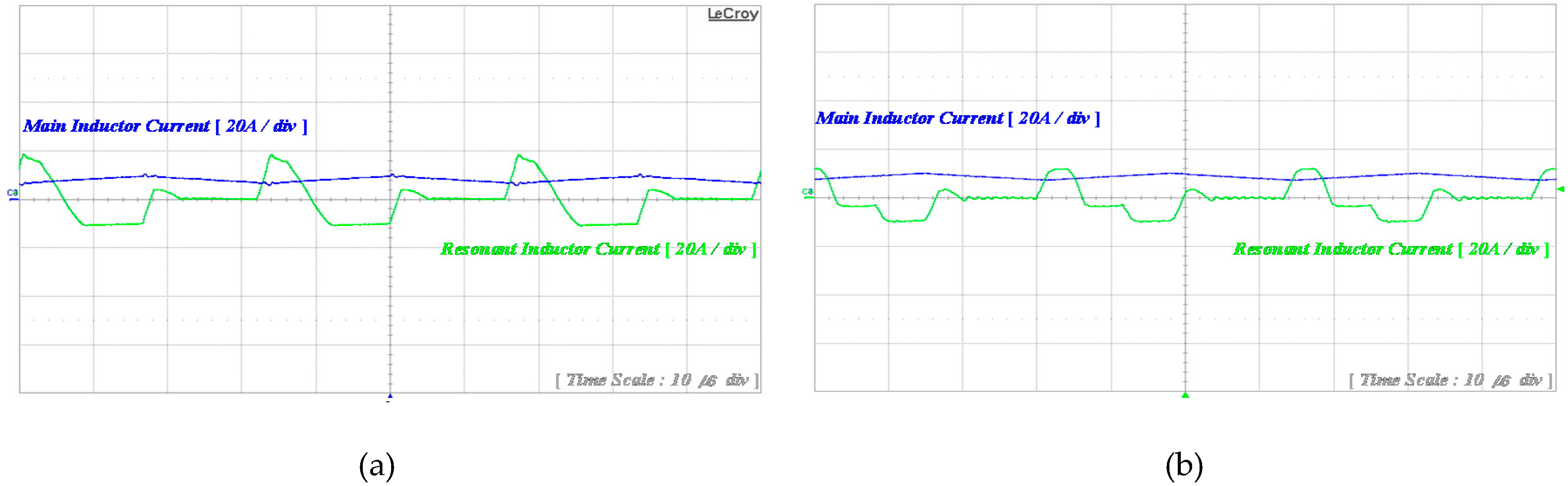
Operation mode of the proposed ZVT resonant boost converter is shown in Figure 3. The operational principle of the proposed converter is divided into ten modes for simple analysis. The mode 1, mode 2 and mode 10 are discharging mode of the proposed ZVT boost converter. The mode 4 made to satisfy the ZVT condition of the main switch S1. And next Mode 5 is turned on under the ZVS condition. And the main inductor charges form mode 5 to mode 9. The mode 3, mode 5, mode 7 and mode 9 operate with resonance. The mode 2, mode 5 and mode 7 are turned on the soft switching of the auxiliary switches.
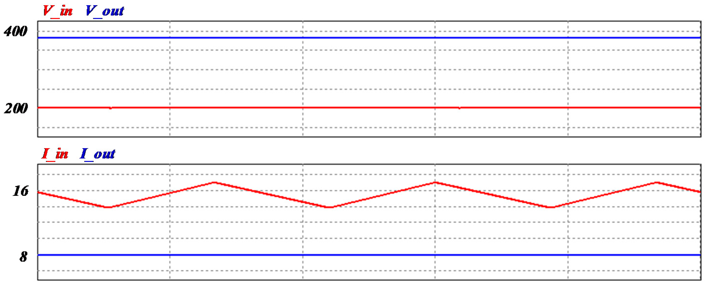
The following statements are assumptions for simple analysis of the proposed converter: First, all switching devices and passive elements (inductor and capacitor) are ideal. Second, the input voltage 200 V and output voltage 380 V are constant. Third, the recovery time of all diodes is ignored. The resonant ZVT boost converters operate in 10 different modes, and the following assumptions were made for a steady-state analysis:
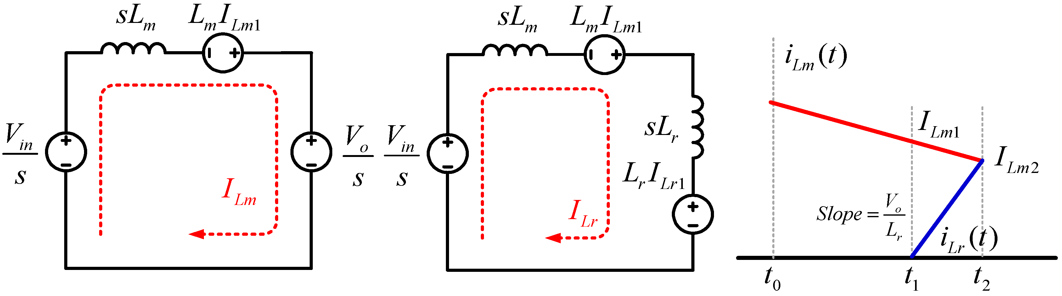
Mode 1 (t0t1): Main S1 and auxiliary switches S2 and S3 are turned off. The accumulated main inductor current Lm is flowed through the output diode Do. Then, output and resonant capacitors Co Cr are charged the same voltage. Equivalent circuit of mode 1 and key waveform is shown in Figure 4. The equivalent circuit shows when the main inductor discharges for boost.
In Mode 1, the main inductor current iLm decreases and the resonant inductor current iLr and auxiliary capacitor voltage vCa are zero. This is expressed as the Equations (1) and (2).
i L m ( t ) = I L m 10 V i n V o L m ( t 0 t 1 )
i L r ( t ) = 0 ,   v C r ( t ) = V o ,   v C a ( t ) = 0
Furthermore, the main inductor current ILm1 is defined for the next mode t2 analysis.
i L m ( t 1 ) = I L m 1
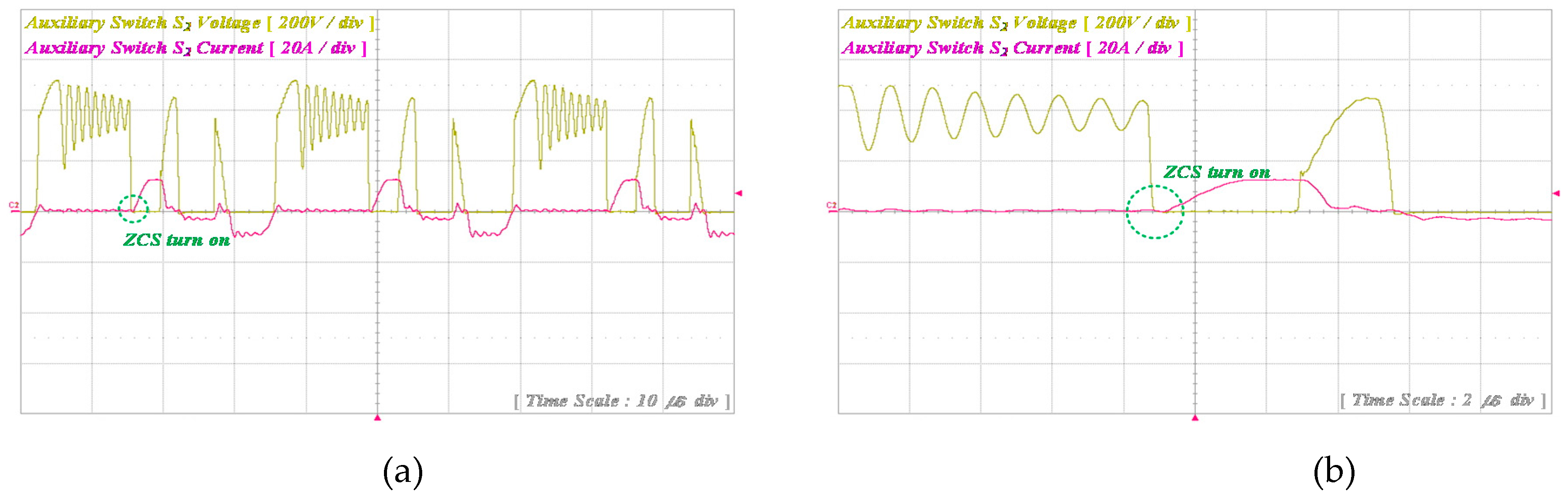
Mode 2 (t1 < t < t2): In Mode 2, an auxiliary switch S2 turns on under the ZCS condition. The resonant inductor current iLr increases linearly from zero. The main inductor current iLm decreases. When the resonant inductor current iLr is equal to the main inductor current iLm, Mode 2 is completed. Also Figure 5 shows an equivalent circuit and key waveform for analyzing mode 2. And the Equivalent circuit Indicates to calculate the magnitude of the current of main inductor iLm and resonant inductor iLr. Thus, the main inductor current is equal to the minimum. The main inductor current iLm and resonant inductor current iLr are expressed by Equations (4) and (5).
i L m ( t ) = I L m 1 V o V i n L m t ,   i L r ( t ) = V o L r t
i L m ( t 2 ) = i L r ( t 2 ) I m i n
The resonant capacitor voltage vCr is equal to output voltage. If parasitic capacitance of resonant switch S3 is ignored, auxiliary capacitor voltage vCa is zero.
v C r ( t ) = V o ,   v C a ( t ) = 0
For Mode 3, the resonant inductor current ILr2 is defined as Equation (7).
i L r ( t 2 ) = V o L r t = I L r 2 = I L m 2
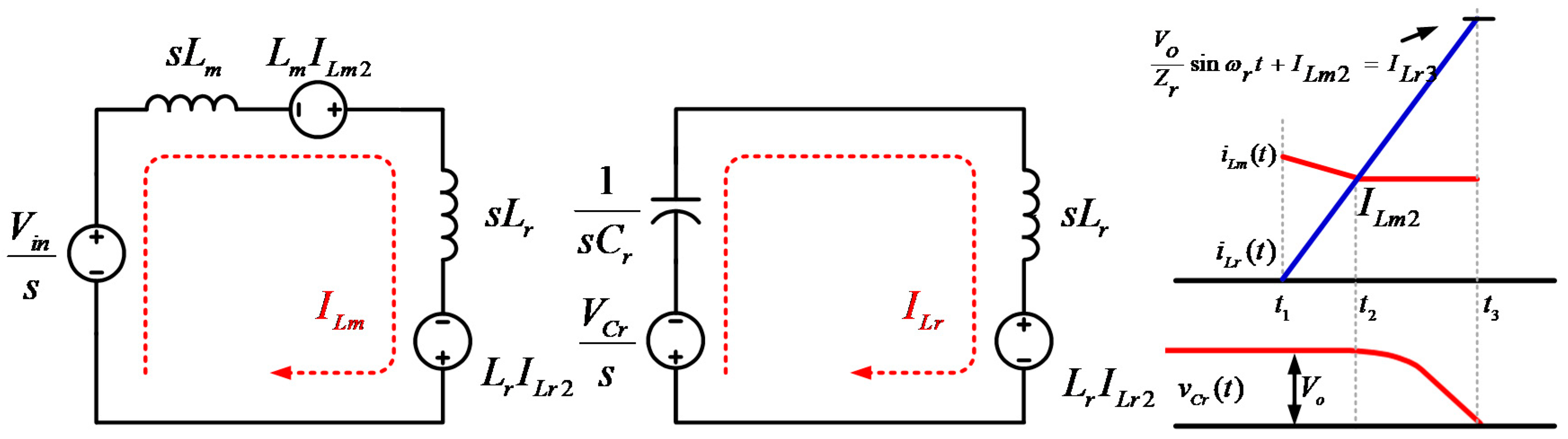
Mode 3 (t2 < t < t3): When the main and resonant inductor currents iLm and iLr are equalized, the resonance operation between resonant capacitor Cr and resonant inductor Lr is started. Then, output diode Do is turned off because the resonant capacitor Cr is discharged. Then, equivalent circuit of resonance operation is shown in Figure 6. The key waveform of mode 3 indicates main inductor current iLm, resonant inductor current iLr and resonant capacitor voltage vCr.
At the end of Mode 3, the resonant capacitor Cr is equal to zero. The resonant capacitor voltage vCr and resonant inductor current iLr can be obtained by the Laplace transform, following Equations (9), (10), (12), and (13). In addition, the resonant impedance Zr and angular frequency ωr are given by Equation (16). Additionally, iLm, iLr, vCa, and vCr are defined by Equations (8), (11), (14), and (15).
i L m ( t ) I m i n
V o s = i L r ( s ) s C r + s L r i L r ( s ) + I m i n
i L r ( s ) = V o L r L r C r 1 L r C r s 2 + ( 1 L r C r ) 2 + I m i n
i L r ( t ) = V o Z r s i n ω r t + I m i n
C r V o = s C r v c r ( s ) + v L C r ( s ) s L r
v C r ( s ) = 1 s C r + 1 s L r C r V o = s s 2 + ( 1 L r C r ) 2 V o
v C r ( t ) = V o c o s ω r t
v C a ( t ) = 0
where
ω r = 1 L r C r , Z r = L r C r
The resonant inductor current ILr3 is defined for the next mode t4 analysis.
i L r ( t 3 ) = V o Z r s i n ω r t + I L r 2 = I L r 3
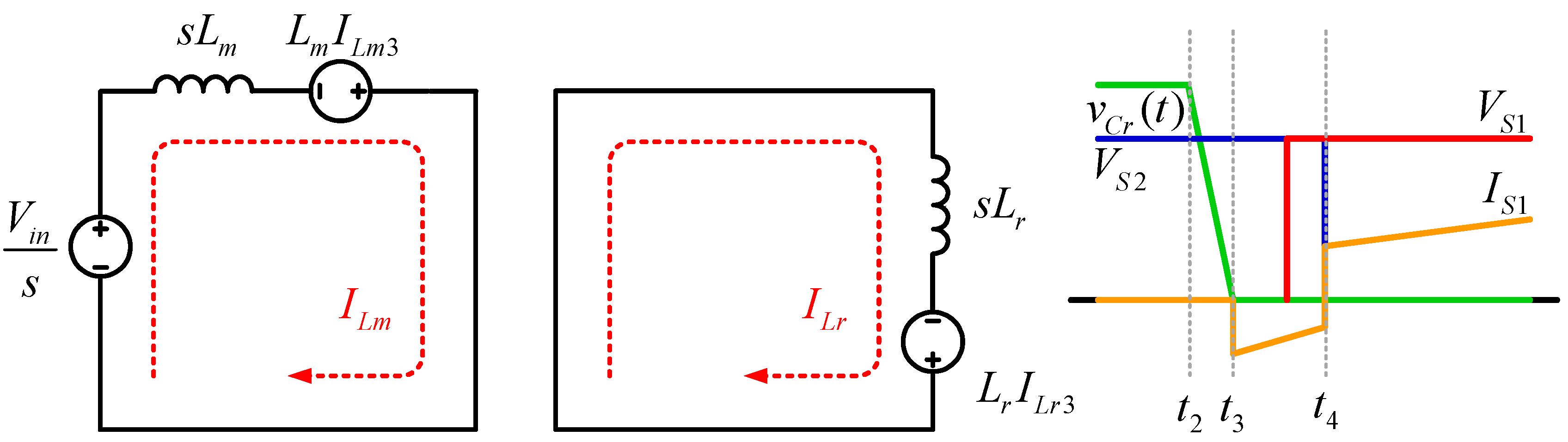
Mode 4 (t3 < t < t4): The body diode of the main switch S1 is turned on, and the voltage of main switch S1 is equal to zero. Then, the main switch S1 is made to satisfy the ZVT condition. Resonant current flows through the anti-parallel diode of the main switch S1. The main inductor current iLm and the resonant inductor current iLr can be derived from Equation (18). Auxiliary and resonant capacitor voltage vCr are all zero by Equation (19). Thus, Figure 7 shows for derivation of the equation. And voltage and current of switches is shown in the key waveform. Mode 4 ends when the auxiliary switch S2 is turned off.
i L m ( t ) = V i n L m t + I m i n ,   i L r ( t ) = I L r 3
v C r ( t ) = 0 ,   v C a ( t ) = 0
Main inductor current ILm4 is defined for the next mode t5 analysis.
i L m ( t 4 ) = V i n L m t + i L m 3 = I L m 4
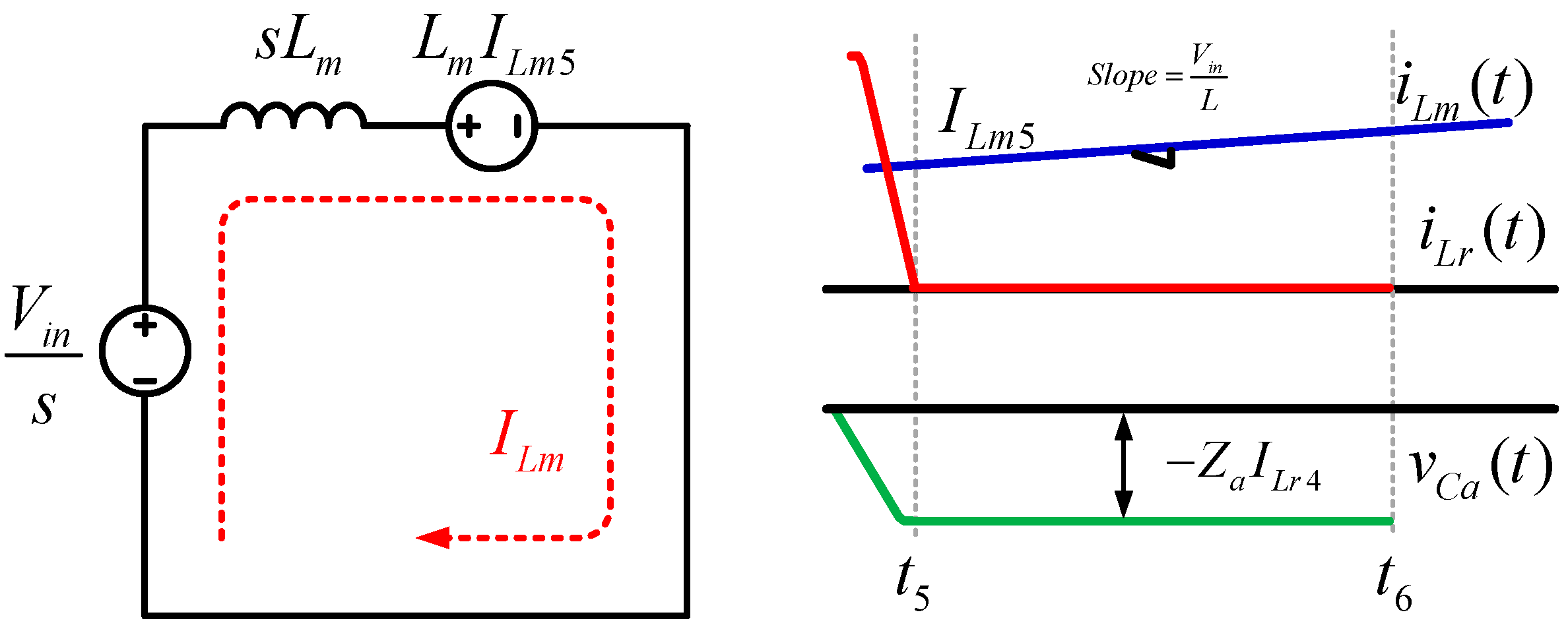
Mode 5 (t4 < t < t5): In Mode 5, the main switch S1 is turned on under the ZVS condition. Then, the main inductor current iLm increases linearly. The auxiliary switch S2 is turned off in the same condition, while the second resonance is begun by the resonant inductor Lr and auxiliary capacitor Ca. Thus, the resonant inductor current iLr decreases. The auxiliary capacitor voltage vCa and resonant inductor current iLr can be derived from the Laplace transform, following Equations (22), (24), and (25). At this time, the equivalent circuit of mode 5 is shown in Figure 8. The equivalent circuit is divided into main inductor current iLm and resonance circuit. The key waveform indicates resonant inductor current iLr, main inductor current iLm and auxiliary capacitor voltage vCa.
Additionally, the resonant impedance Za and angular frequency ωa are given by Equation (27). Then, iLm, iLr, vca, and vCr are defined by Equations (21), (23), and (26).
i L m ( t ) = V i n L m t + I L m 4
i L r ( s ) = L r I L r 4 1 s C a + s L r = s s 2 + ( 1 L r C r ) 2 I L r 4
i L r ( t ) = I L r 4 c o s ω a t
I L r 4 s = v C a s L r + v C a s C a
v C a ( s ) = L r C a 1 L r C a s 2 + ( 1 L r C a ) 2 I L r 4
v C a ( t ) = Z a I L r 4 s i n ω a t
where
ω a = 1 L r C a Z a = L r C a
For Mode 6, the resonant inductor current iLr and auxiliary capacitor voltage vCa are defined as Equation (28).
i L r ( t 5 ) = 0 = I L r 5 ,   v C a ( t 5 ) V o
Mode 6 (t5 < t < t6): In Mode 6, resonant inductor Lr and auxiliary capacitor Ca end the second resonant operation and the resonant capacitor Ca is charged. The main inductor current iLm increases linearly through the main switch S1. Mode 6 ends when the auxiliary switch S3 turns on. The equivalent circuit of mode 6 and key waveform is shown in Figure 9. The main inductor current iLm can be calculated through the equivalent circuit. The iLm, iLr, vCa, and vCr values are as follows in Equations (29) and (30):
i L m ( t ) = V i n L m t + I L m 5 ,   i L r ( t ) = 0
v C a ( t ) = V o ,   v C r ( t ) = 0
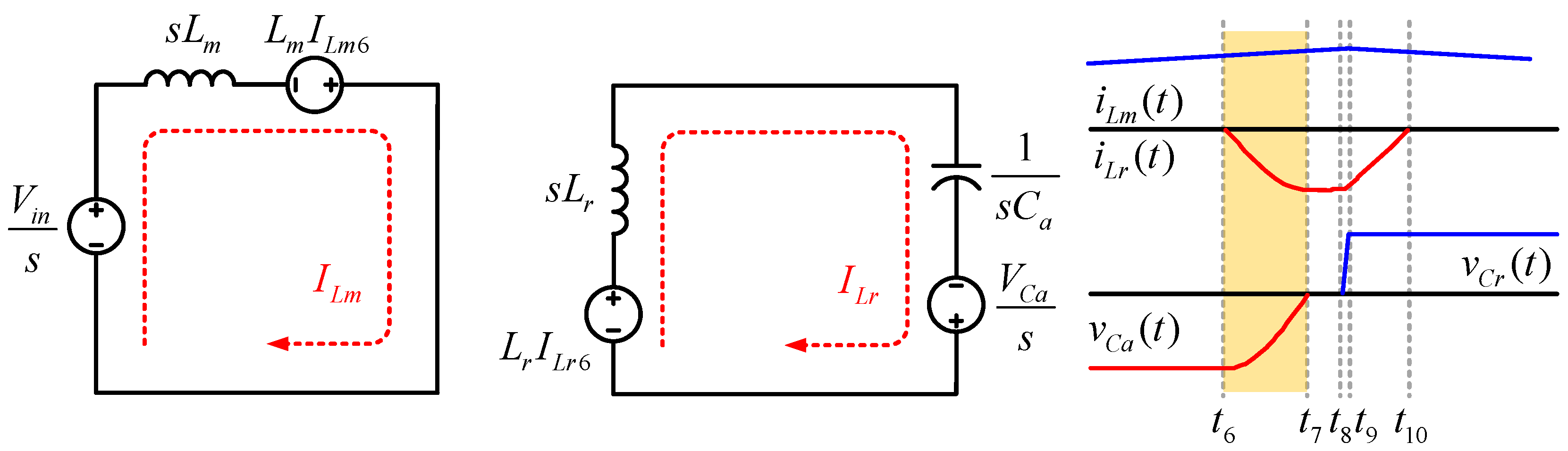
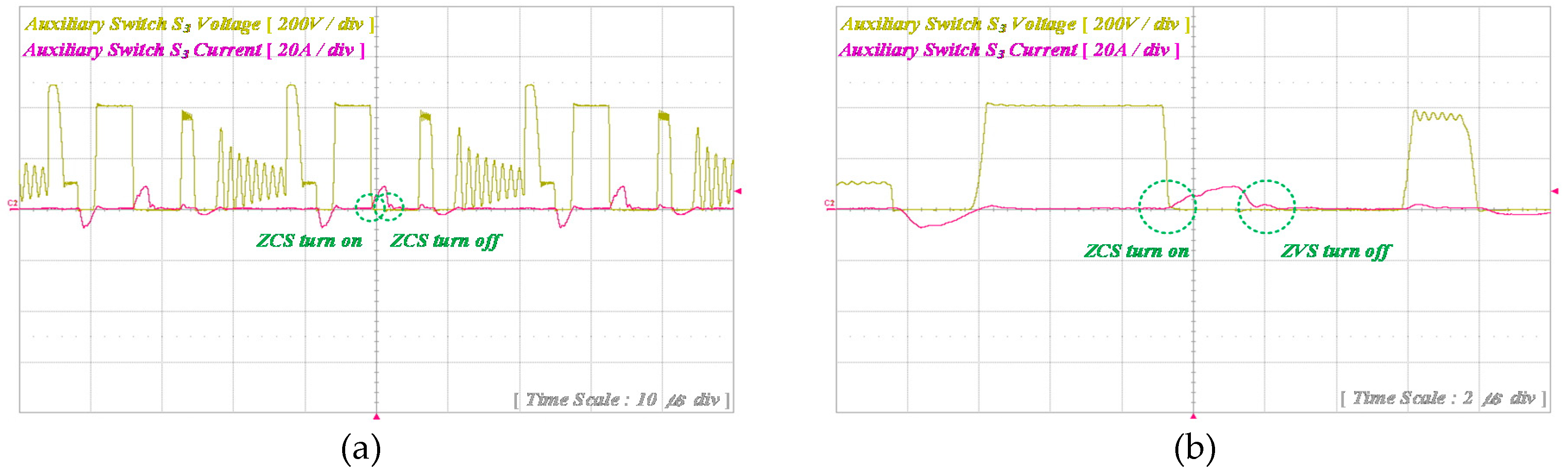
Mode 7 (t6 < t < t7): At the beginning of Mode 7, the third resonance begins. Then, the auxiliary switch S3 turns on under the ZCS condition. The energy stored in the resonant capacitor Cr is transferred to the resonant inductor through auxiliary switch S3. The auxiliary capacitor voltage vCa and resonant inductor current iLr can be derived from the Laplace transform, following Equations (32), (33), (35), and (36). Then, the equivalent circuit is shown in Figure 10. Mode 7 ends when the auxiliary capacitor Ca voltage reaches 0 V, as in Equation (38). The current that flows through the main inductor Lm increases linearly, as in Equation (31) and the energy is stored in the resonant inductor Lr through the auxiliary switch S3. The iLr and vca values were defined by Equations (34) and (37).
i L m ( t ) = V i n L m t + I L m 6
Z a I L r 4 s = i L r ( s ) s C a + s L r i L r ( s )
i L r ( s ) = Z a I L r 4 L r L r C a 1 L r C a s 2 + ( 1 L r C a ) 2
i L r ( t ) = I L r 4 s i n ω a t
C a Z a I L r 4 = v C a ( s ) s C a + v C a ( s ) s L r
v C a ( s ) = s s 2 + ( 1 L r C a ) 2 Z a I L r 4
v C a ( t ) = Z a I L r 4 c o s ω a t
v C r ( t ) = 0
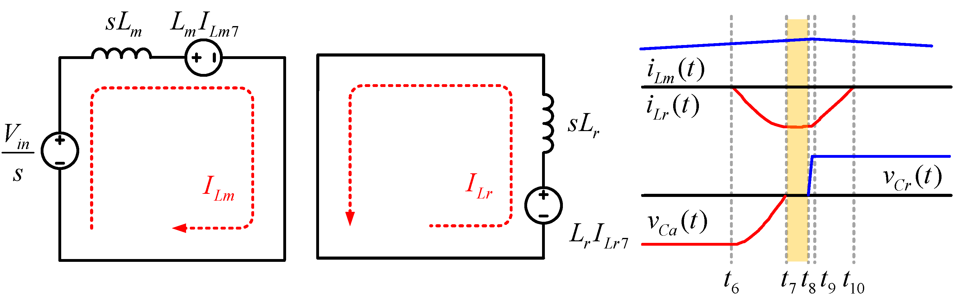
Mode 8 (t7 < t < t8): In Mode 8, the auxiliary capacitor voltage vCa becomes zero. Then, the main inductor current iLm increases linearly and the body diode of the auxiliary switch S2 is turned on. The resonant inductor Lr current flows through the freewheeling path of the body diode—the main switch S1. When the main switch S1 is turned off, Mode 8 is complete. In this interval, the magnitude of the resonant inductor current iLr is equal to that of Mode 3. However, the current flow is reversed. The iLm, iLr, vCa, and vCr values are as follows in Equations (39) and (40):
i L m ( t ) = I L m 7 + V i n L t ,   i L r ( t 8 ) = i L r 7
v C a ( t ) = 0 ,   v C r ( t ) = 0
The equivalent circuit of mode 8 and key waveform is shown Figure 11. The equivalent circuit is divided into main inductor current iLm and resonant inductor current iLr. The key waveform indicates iLm, iLr, vCa, and vCr.
For Mode 9, the main and resonant current ILm8 are defined by Equations (41) and (42).
i L m ( t 8 ) = V i n L m t + I L m 7 = I L m 8
i L r ( t 8 ) = I L r 7 = I L r 8
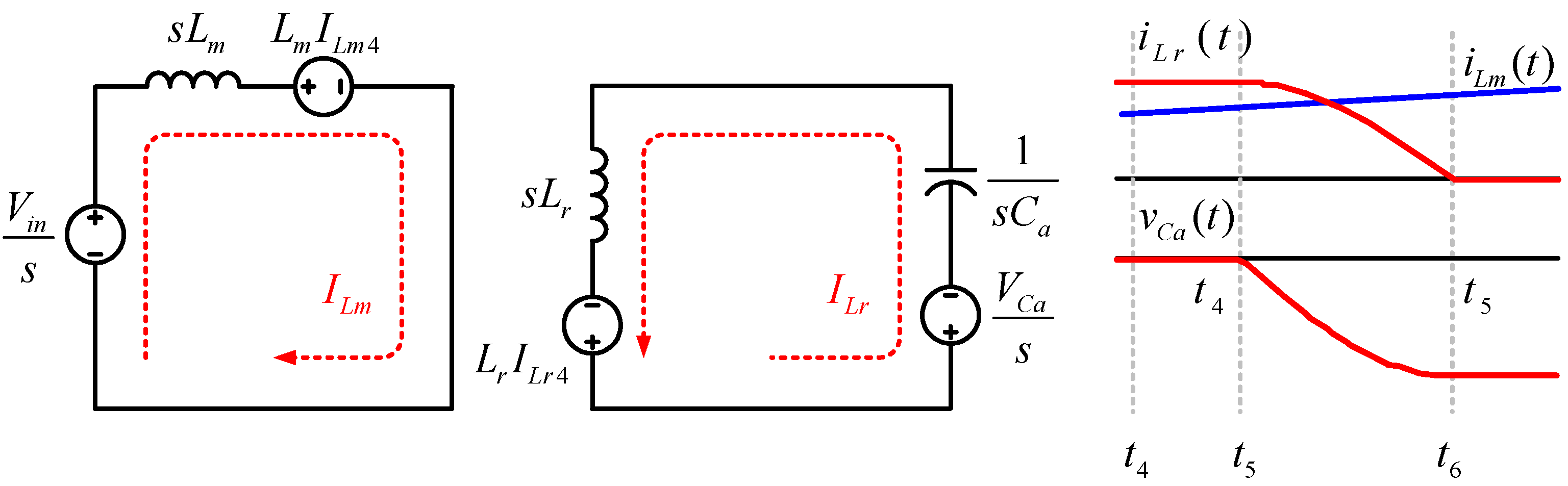
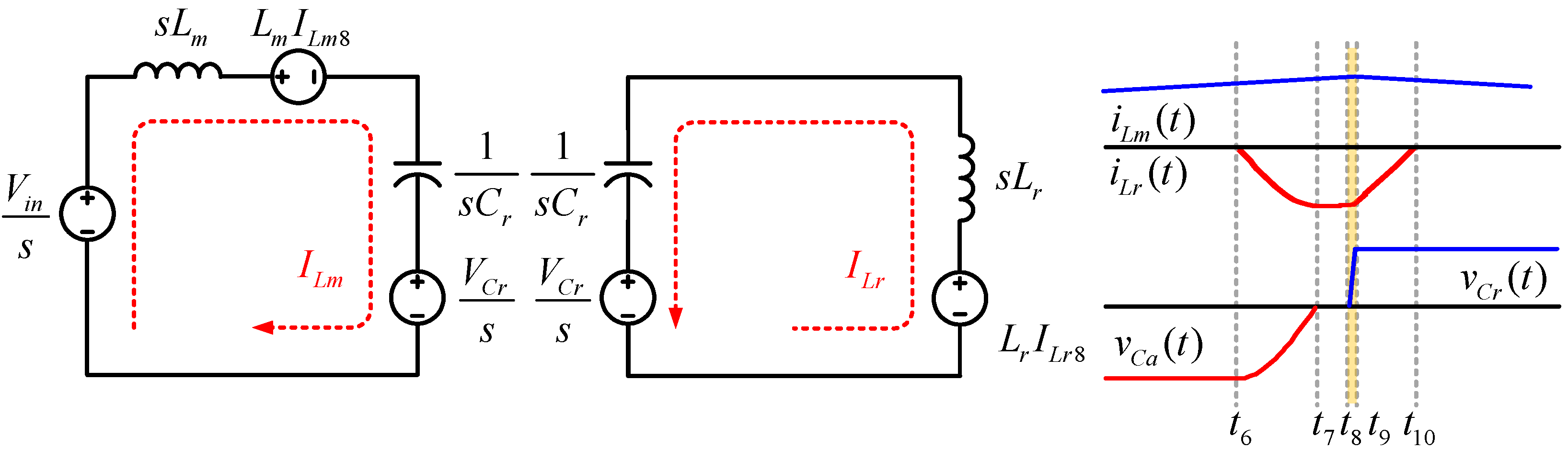
Mode 9 (t8 < t < t9): In this mode, the fourth resonance between the resonant inductor Lr and the resonant capacitor Cr begins. The current that flows in the resonance inductor Lr is reduced from the maximum point and the resonant capacitor Cr is charged by the total current of the main and resonant inductor. Then, the voltage of the resonant capacitor vCa is charged to the output voltage Vo, and Mode 9 ends. The resonant capacitor voltage vCa and resonant inductor current iLr can be derived from the Laplace transform, following Equations (44), (45), (47), and (48). The iLm, iLr, vCa, and vCr values are as follows in Equations (43), (46), (49), and (50):
i L m ( t ) = I L m 8
L r ( I L r 8 ) = i L r ( s ) s C r + i L r ( s ) s L r
i L r ( s ) = s s 2 + ( 1 L r C r ) 2 ( I L 8 )
i L r ( t ) = I L 8 c o s ω r t
I L 8 s = v C r ( s ) s L r + v C r ( s ) s C r
v C r ( s ) = L r C r 1 L r C r s 2 + ( 1 L r C r ) 2 ( I L 8 )
v C r ( t ) = Z r I L r 8 s i n ω r t
v C a ( t ) = 0
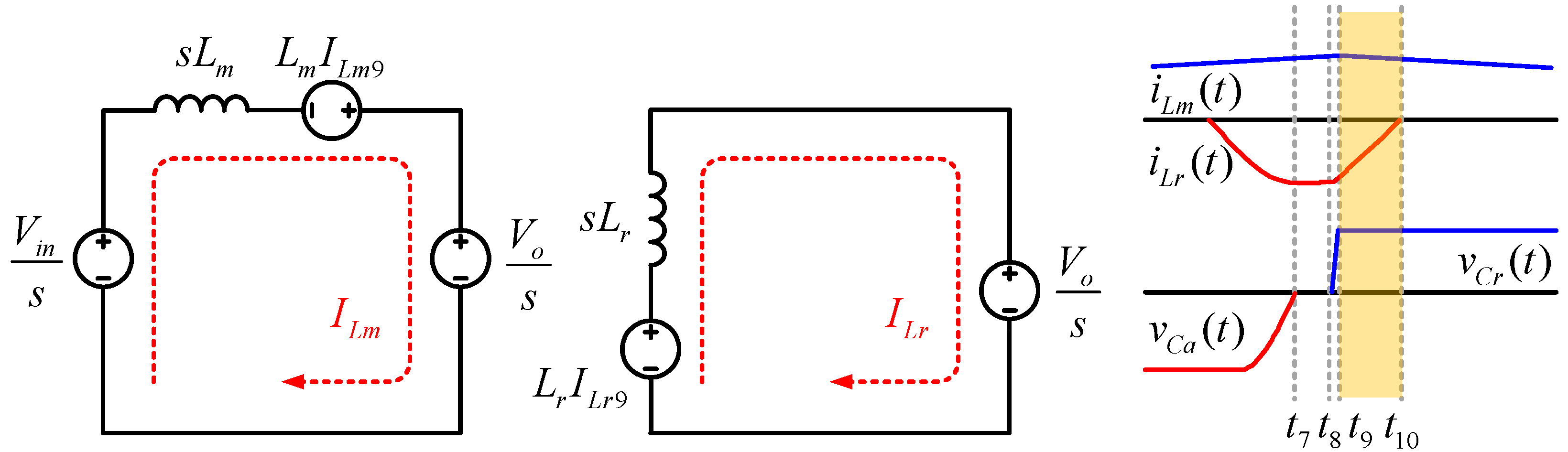
The Mode 9 is divided into two equivalent circuits in Figure 12. Then, the equivalent circuit of resonance operation is shown. The key waveform of Mode 9 indicates iLm, iLr, vCa, and vCr. And the key waveform of Figure 12 shows the maximum of the main inductor current iLm.
For Mode 10, the main inductor current ILm9 is defined:
i L m ( t 9 ) = I L m 8 = I L m 9
Mode 10 (t9 < t < t10): The resonant inductor current iLr linearly decreases to zero. And if the resonant capacitor voltage vCa is charged with a larger output than output voltage Vo, then the output diode Do is turned on. Mode 10 is completed, and the next switching cycle starts.
The Mode 10 is divided into two equivalent circuits in Figure 13. Then, the equivalent circuit of main inductor Lm is shown. Other equivalent circuit indicates resonant inductor Lr. The key waveform of Figure 13 shows the maximum of the main inductor current iLm. And resonant capacitors Cr are charged the output voltage.
i L m ( t ) = I L m 9 V o V i n L t
i L r ( t ) = I L r 9 V o L r t
v C r ( t ) = V o ,   v C a ( t ) = 0

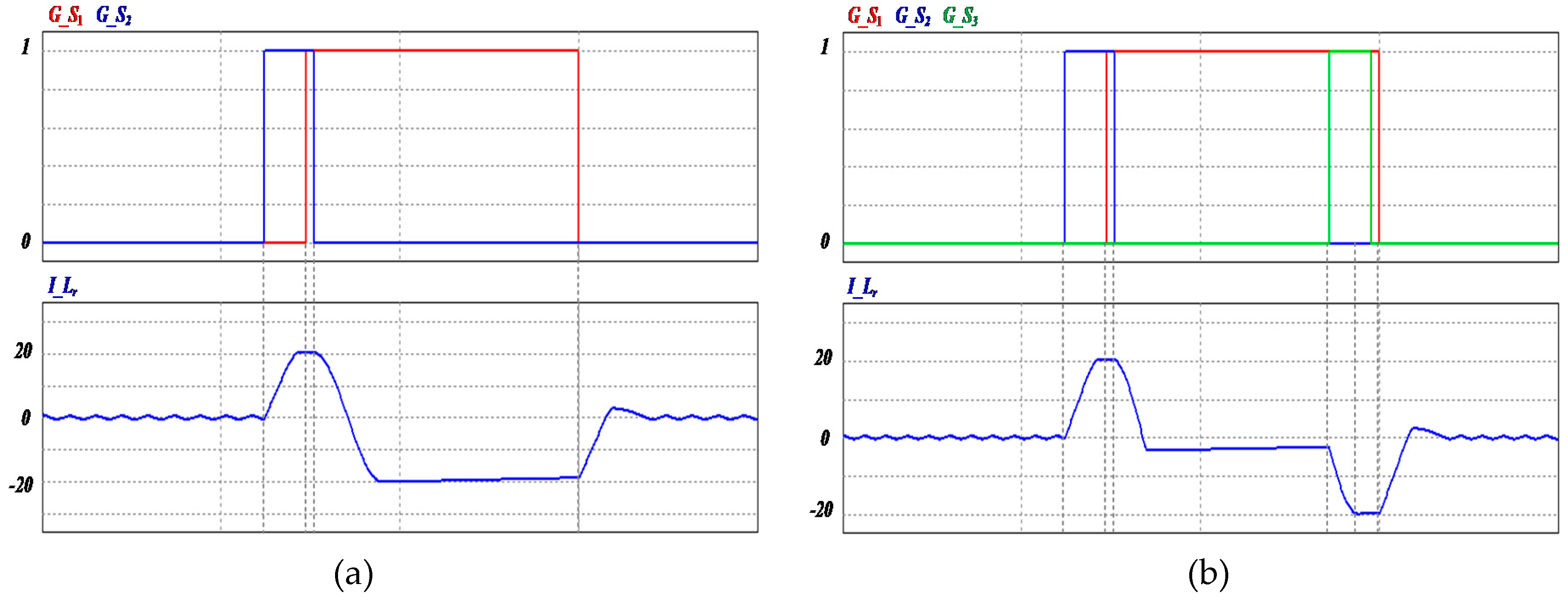
2.3. PWM Signal Analysis

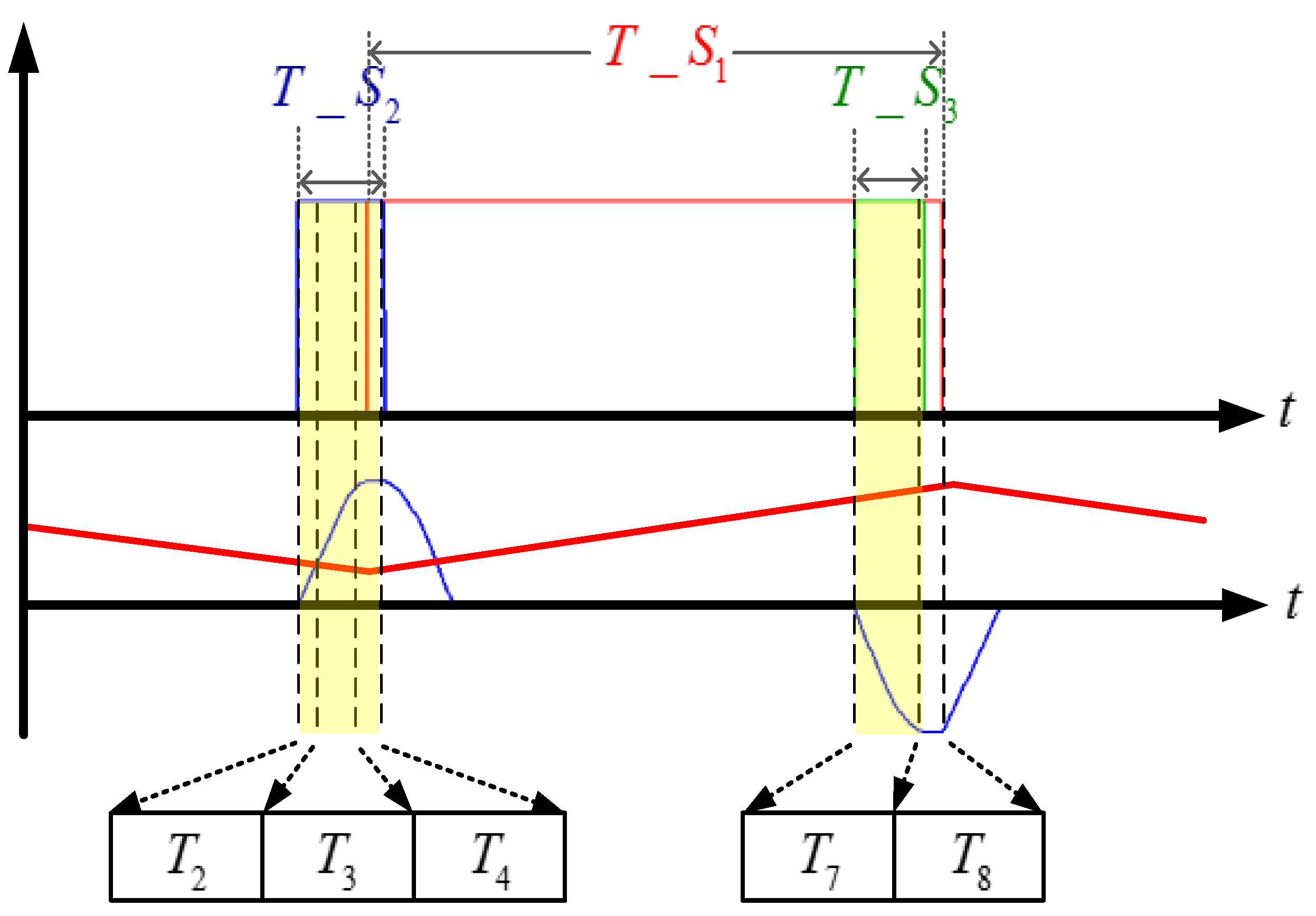
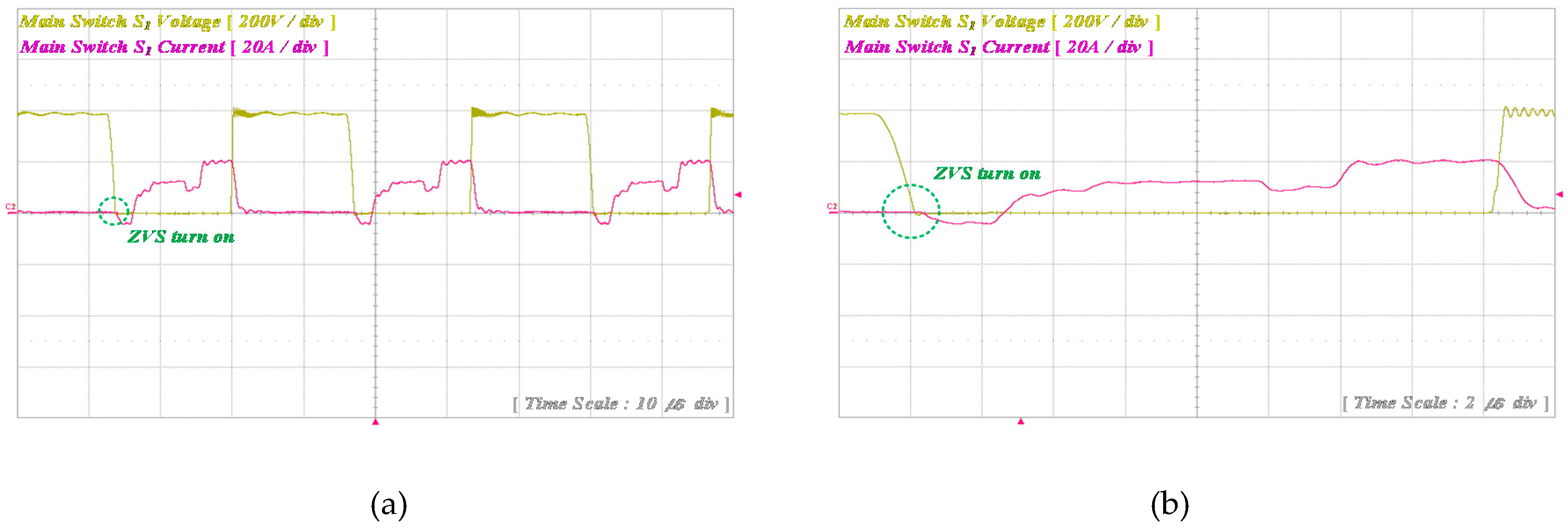
PWM signals of the main and auxiliary switch are shown in Figure 14. The auxiliary switch S2 is turned on before the main switch S1 is turned on. Then turning on interval of the auxiliary switch S2 can be divided into mode 2, mode 3 and mode 4. The main switch S1 makes boost at turning on and turning off. The auxiliary switch S3 operates to reduce conduction loss. And turning on interval of the auxiliary switch S3 can be shown into mode 7.
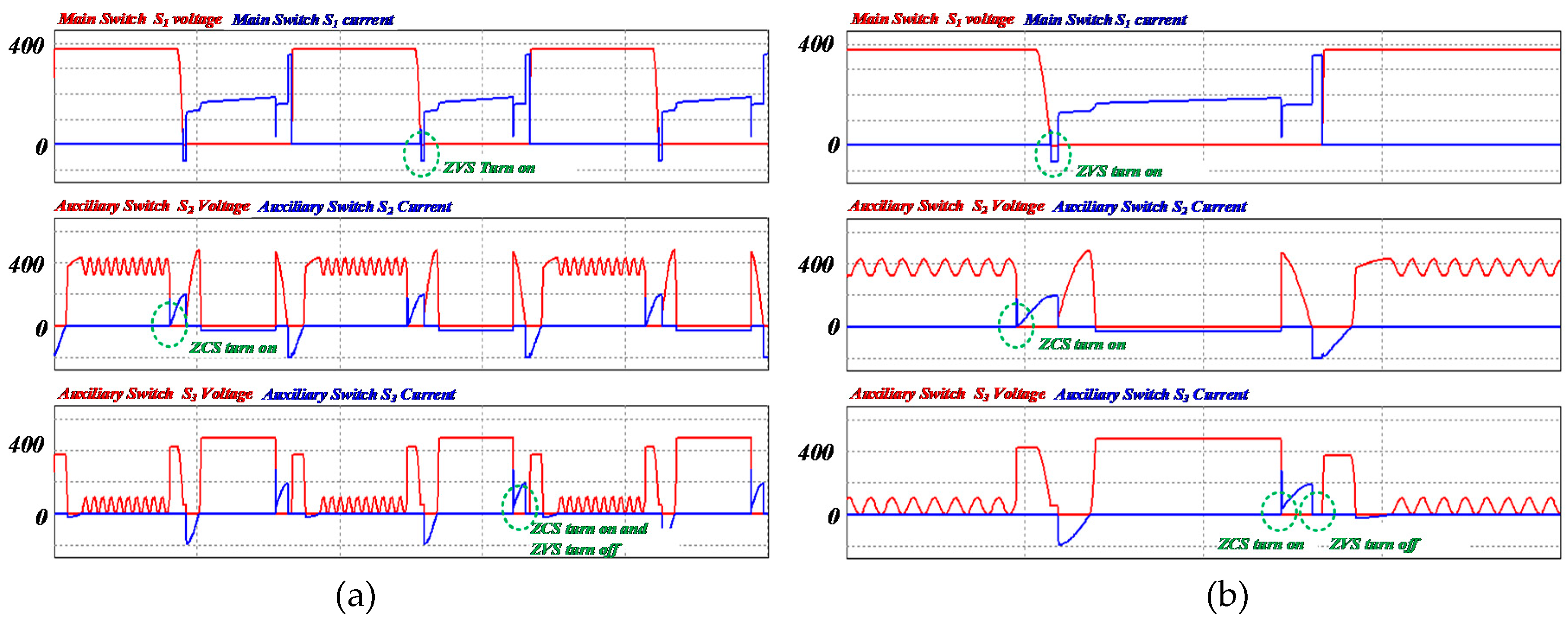
This design for a proposed resonant ZVT boost converter is composed of three switches, and the minimum turn-on and turn-off time should be satisfied in order to achieve ZVS and ZCS. The main switch controls the step-up ratio. Other auxiliary switches enable the main switch to operate with a soft switching. The resonances for the resonant inductor Lr and the resonant capacitor Cr are started by turning on the auxiliary switch S2. When the charged energy completely discharges from the resonant capacitor, the main switch S1 turns on in the ZVS condition. Before the main switch S1 turns on, the auxiliary switch S2 is turned on and turned off. To achieve the ZVS, a minimum time of auxiliary switch pulse width modulation (PWM) is required. The time is determined by Mode 2, Mode 3, and Mode 4. The T2, T3, and T4 time must be satisfied according to the following equation:
T 2 = I L m .1 L m L r V i n L r V o ( L m + L r )
T 3 = sin 1 ( sin ω r t ) 2 π F r
F r = 1 2 π L r C r
T4 is determined by using a factor of k from the time delay of the switching elements.
T 4 = t × k
t < L m ( I L r 3 I L m 3 ) V i n
The turning on and off times for the auxiliary switch S2 can be satisfied, as shown in the following Equation (60):
T S 2 > T 2 + T 3 + T 4
Before the main switch is turned off, the auxiliary switch S3 is turned on and off. After the energy for the resonant inductor Lr discharges and reaches zero, the auxiliary switch S3 turns on. The auxiliary switch S3 turns on in the ZCS condition. After the auxiliary capacitor Ca discharges, the auxiliary switch S3 turns off in the ZVS condition. The turning on and off times for the auxiliary switch S3 can be calculated by using the equations for Modes 7 and 8. T7 requires a longer time than half the secondary resonant auxiliary frequency and T8 requires a longer time than the off-delay time of the elements, which can be obtained from the manufacturer’s data sheet. The shortest time for the auxiliary switch S3 should be satisfied by using the following Equations (61)–(63).
T 7 = T r 2 = π L r C a
T 8 > t d ( o f f )
T S 3 > T 7 + T 8

2.4. Resonant Device Design

Resonant capacitor Cr influences the ZVS operation of the main switch S1. The ZVS switching process can be performed when the resonant capacitor Cr is sufficiently charged [16]. Thus, the design of resonant capacitors Cr is important. When the resonant capacitor Cr is charged and discharged in Mode 3 and Mode 9, the resonant time between the resonant inductor Lr and resonant capacitor Cr can be expressed as the following equation:
T m o d e 3 = π 2 L r C r
In Mode 9, resonant capacitor Cr is charged to output voltage and can be expressed as the following equation:
T m o d e 9 = C r V o 2 I i n _ m a x
Assume that the maximum current of the resonant inductor is Iin_max, and the sum of the two inductor currents is the charging current of the resonant capacitor Cr. When Mode 9 is longer than Mode 3, the defective duty ratio is lower. Thus, the time is chosen as 0.1 Ts. The sum of Mode 3 and Mode 9 is selected as 1/10 of one cycle. The charging time of the resonant capacitor Cr must be longer for ZVS of the main switch. For this reason, the value of the resonant capacitor Cr should be chosen to be 15 times larger than that of the output switch capacitor. According to the output capacitance of main switch S1, a suitable value of the resonant capacitor is 0.6 nF. The output capacitance of the main switch S1 is given in the manufacturer’s data sheet. As a result, resonant capacitor Cr used 10 nF to consider a margin of error.
π 2 L r C r + C r V o 2 I i n _ m a x 0.1 T s
In addition, the resonant current between the resonant inductor Lr and resonant capacitor Cr charges the auxiliary capacitor Ca. The resonant time between the resonant inductor Lr and auxiliary capacitor Ca in Mode 5 and Mode 7 is set as one-fifth of the total turning on time. If the charging voltage of this resonant capacitor Cr is too large, it may be voltage stress. The auxiliary capacitance was calculated to be 39 nF. The auxiliary capacitor used 40 nF to consider a margin of error.
Resonance between resonant inductor Lr and capacitor Cr operates for soft switching of the main switch. Then, the main switch S1 has satisfied the ZVT condition. Resonance design is very important to satisfy ZVS, ZCS, and ZVT [17]. But if the resonant inductor current iLr continues to increase linearly, the magnetic flux of the inductor is saturated [18]. Thus, the flux of the inductor must be prevented from reaching saturation, using the auxiliary capacitor Ca. The auxiliary capacitor Ca is charged from the negative current of the resonant inductor. In this case, energy relation can be defined by auxiliary capacitor Ca and resonant inductor Lr. Therefore, stored energy of the inductor is equal to or greater than the stored energy of the capacitor.
The resonant capacitor Lr must charge below the output voltage Vo. Obtained values in each mode can be expressed by the following Equations (67) and (68) [19,20,21]:
1 2 L r I L r _ m a x 2 1 2 C a V o 2
C a L r I L r _ m a x 2 V o 2

3. Simulation Results

The computer was simulated to verify the operation of the new ZVT boost converter design. The design specifications of the elements used in the simulation are shown in Table 1. This paper tested the proposed converter by POWERSIM Inc. PSim9.2 software. The simulation time step has 1E-007 for detailed waveform analysis. The design specifications of the elements used in the simulation are shown in Table 1. The simulation was performed under a 30-kHz switching frequency and a 200–380 V voltage.
The waveform of each PWM signal is shown in Figure 15 and the resonant inductor current iLr flows according to each PWM signal.
The current conduction period of the proposed converter is shorter than the conventional converter. The waveforms of the voltage and current of each switch are shown in Figure 16. The soft switching operations of each switch were successfully performed, as shown in Figure 16b. It also shows some voltage ringing, due to the resonance between the auxiliary switches S2 and S3. The switch used in the simulation is non-ideal, and the parasitic capacitances may cause a switch failure. Specifically, the output capacitance resonates with the resonance inductor and leads to ringing. These resonances may cause the current or voltage stress on the devices and finally increase the voltage rating of the devices.
Figure 17 shows the waveforms of the input and output of the voltage and current. The proposed ZVT boost converter can be applied to the photovoltaic system of DC distribution. Therefore, the output of the proposed converter can be directly connected to the DC voltage of the DC distribution building.

4. Experimental Results

In order to prove the theoretical analysis, experiments were conducted on the proposed ZVT boost converter in Figure 18. It consists of a boost converter, a controller, and a gate driver. The controller used in this experiment was the DSP TMS320F28335 from TI.
The experiment was conducted with the 4 kW, 30 kHz converter, which steps up the voltage from 200 V to 380 V.
To compare the conventional and the proposed converter, current waveforms of the main inductor and the resonant inductor are shown in Figure 19. When the main switch S1 is turned on, the current through the main inductor Lm increases linearly. When the main switch S1 is turned off, the energy that was stored in the main inductor Lm is released through the output diode Do and is transferred to the load. The same kinds of waveforms are shown in Figure 2. Conduction periods of the conventional converter were observed to be larger than those for the proposed converter.
The waveforms for the voltage and current across the main switch S1 are shown in Figure 20. Before the main switch S1 is turned on, the body diode of the main switch has a freewheeling period. Then, the main switch is turned on under ZVS in the ZVT condition. The waveforms for the voltage and current across the main switch S1 are shown in Figure 20. Figure 20b is a close up of the soft switching in voltage and current of the main switch S1.
The waveforms for the voltage and the current across the auxiliary switch S2 are shown in Figure 21. The auxiliary switch S2 is turned on under the ZCS condition because of the resonant inductor. Thus, the current of the auxiliary switch S2 increases linearly from zero. The voltage of the auxiliary switch S2 is equal to zero and the auxiliary capacitor Ca does not affect the auxiliary switch S2. Thus, the waveforms of the auxiliary switch S2 are shown by a negative resonant inductor auxiliary capacitor and a resonant operation. Figure 21b shows an extension of the soft switching of the auxiliary switch S2.
Figure 22 shows the waveforms for the voltage and current across the auxiliary switch S3. The body diode of the main switch is turned on under a zero-voltage switching condition. Afterwards, the auxiliary switch S3 is turned on under the ZCS condition because of the resonant inductor Lr and auxiliary capacitor Ca. Then, voltage of the auxiliary switch S3 remains at zero. Figure 22b shows the extension of soft-switching for the auxiliary switch S3. Voltage ringing occurs due to the resonance between the auxiliary switches S2 and S3. The switch used in the simulation is non-ideal, and the parasitic capacitances may cause a switch failure. Specifically, the output capacitance resonates with the resonance inductor and leads to ringing.
The input/output voltage and current waveforms are shown in Figure 23. A voltage step-up occurs from an input voltage of 200 V to an output voltage of 380 V, indicating good control of the output voltage.
The efficiency comparison of the conventional (C) and proposed (P) converter is shown in Table 2. A power analyzer (model WT-3000) was used to confirm the efficiency of the proposed converter. The output power 380 V and the input power 200 V were fixed while measuring variable loads, based on a rated capacity of 4 kW. According to the efficiency measurements, a measured full-load efficiency of over 90% was confirmed, and a maximum efficiency of 96.5% was measured at 95% load.

5. Conclusions

In this paper, the resonant ZVT boost DC–DC converter, which uses the auxiliary resonant circuit, is proposed. All switches of the proposed converter were operated under ZVS and ZCS. Thus, the switching losses were reduced by using the resonant circuit. It is composed of two switches, the resonant inductor and two resonant capacitors. Furthermore, the proposed converter reduces the conduction loss of the resonant inductor, compared to the conventional converter. As a result, the proposed converter improves the whole system’s efficiency better than the conventional converter at the same frequency. To verify, the experiment was successful. The measured efficiency of the proposed converter is 96.5%, which is a highly improved result, compared to the conventional resonant converter at 94.2%. In addition, based on mathematical modeling, the equivalent circuit of each operation mode was analyzed. Operation modes were divided, considering the current and voltage waveforms. The simulation was performed to verify the validation of the proposed converter. To conclude, the simulation and experimental results were the same.
Therefore, the proposed high-efficiency converter is suitable for applications such as photovoltaic converters of DC distribution and sensor systems.

Author Contributions

Conceptualization, H.J.L. and Y.-H.K.; Formal Analysis, H.J.L.; Supervision, Y.-H.K.

Funding

This research received no external funding.

Conflicts of Interest

The authors declare no conflict of interest.

Nomenclature

LmMain Inductor
LrResonant Inductor
CrResonant Capacitor
CaAuxiliary Capacitor
DoOutput Diode
S1Main Switch
S2Auxiliary Switch 2
S3Auxiliary Switch 3
iLmMain Inductor Current
iLrResonant Inductor Current
vCrResonant Capacitor Voltage
vCaAuxiliary Capacitor Voltage
iDoOutput Diode Current

References

  1. Tsai, C.H.; Su, J.Y. A Soft-Switching SEPIC with Multi-Output Sources. Electronics 2017, 6, 35. [Google Scholar] [CrossRef]
  2. Lin, B.-R. Investigation of a Resonant dc–dc Converter for Light Rail Transportation Applications. Energies 2018, 11, 1078. [Google Scholar] [CrossRef]
  3. Lee, H.J.; Shin, S.C.; Hong, S.J.; Hyun, S.W.; Lee, J.H.; Won, C.Y. Performance Improvement of Isolated High Voltage Full Bridge Converter Using Voltage Doubler. J. Electr. Eng. Technol. 2014, 9, 2224–2236. [Google Scholar] [CrossRef]
  4. Kim, Y.H.; Ji, Y.H.; Kim, J.G.; Jung, Y.C.; Won, C.Y. A New Control Strategy for Improving Weighted Efficiency in Photovoltaic AC Module-Type Interleaved Flyback Inverters. IEEE Trans. Power Electron. 2013, 28, 2688–2699. [Google Scholar] [CrossRef]
  5. Kim, Y.H.; Jang, J.W.; Shin, S.C.; Won, C.Y. Weighted-Efficiency Enhancement Control for a Photovoltaic AC Module Interleaved Flyback Inverter Using a Synchronous Rectifier. IEEE Trans. Power Electron. 2014, 29, 6481–6493. [Google Scholar] [CrossRef]
  6. Xue, J.; Lee, H. Enabling High-Frequency High-Efficiency Non-Isolated Boost Converters With Quasi-Square-Wave Zero-Voltage Switching and On-Chip Dynamic Dead-Time-Controlled Synchronous Gate Drive. IEEE Trans. Power Electron. 2015, 30, 6817–6828. [Google Scholar] [CrossRef]
  7. Moshirvaziri, M.; Li, C.; Trescases, O. A quasi-resonant bi-directional tri-mode DC-DC converter with limited valley current. In Proceedings of the Twenty-Seventh Annual IEEE Applied Power Electronics Conference, Coronado, CA, USA, 5–9 February 2012; pp. 517–523. [Google Scholar] [CrossRef]
  8. Liu, Y.C.; Chen, M.C.; Yang, C.Y.; Kim, K.A.; Chiu, H.J. High-Efficiency Isolated Photovoltaic Micro inverter UsingWide-Band Gap Switches for Standalone and Grid-Tied Applications. Energies 2018, 11, 569. [Google Scholar] [CrossRef]
  9. Pilawa-Podgurski, R.C.N.; Sagneri, A.D.; Rivas, J.M.; Anderson, D.I.; Perreault, D.J. Very High Frequency Resonant Boost Converters. In Proceedings of the IEEE 38th Annual Power Electronics Specialists Conference, Orlando, FL, USA, 17–21 June 2007; pp. 2718–2724. [Google Scholar] [CrossRef]
  10. Cheng, X.F.; Zhang, Y.; Yin, C. A ZVS Bidirectional Inverting Buck-Boost Converter Using Coupled Inductors. Electronics 2018, 7, 221. [Google Scholar] [CrossRef]
  11. Urgun, S. Zero-voltage transition–zero-current transition pulse width modulation DC–DC buck converter with zero-voltage switching‣zero-current switching auxiliary circuit. IET Power Electron. 2012, 5, 627–634. [Google Scholar] [CrossRef]
  12. Mahesh, M.; Panda, A.K. High-power factor three-phase ac–dc soft-switched converter incorporating zero-voltage transition topology in modular systems for high-power industry applications. IET Power Electron. 2011, 4, 1032–1042. [Google Scholar] [CrossRef]
  13. Phattanasak, M. A ZVT boost converter using an auxiliary resonant circuit. In Proceedings of the Power Electronics, Drives and Energy Systems, New Delhi, India, 12–15 December 2006; pp. 1–6. [Google Scholar] [CrossRef]
  14. Khorasani, R.R.; Adib, E.; Farzanehfard, H. ZVT Resonant Core Reset Forward Converter with a Simple Auxiliary Circuit. IEEE Trans. Ind. Electron. 2018, 65, 242–250. [Google Scholar] [CrossRef]
  15. Park, S.H.; Park, S.R.; Yu, J.S.; Jung, Y.C.; Won, C.Y. Analysis and design of a soft-switching boost converter with an HI-bridge auxiliary resonant circuit. Trans. Power Electron. 2010, 25, 2142–2149. [Google Scholar] [CrossRef]
  16. Han, D.W.; Lee, H.J.; Shin, S.C.; Kim, J.G.; Jung, Y.C.; Won, C.Y. A new soft switching ZVT boost converter using auxiliary resonant circuit. In Proceedings of the IEEE Vehicle Power and Propulsion Conference, Seoul, Korea, 9–12 October 2012; pp. 1250–1255. [Google Scholar] [CrossRef]
  17. Mercorelli, P.; Werner, N. An Adaptive Resonance Regulator Design for Motion Control of Intake Valves in Camless Engine Systems. IEEE Trans. Ind. Electron. 2017, 64, 3413–3422. [Google Scholar] [CrossRef]
  18. Schimmack, M.; Costa, M.L.; Mercorelli, P. Comparing Two Voltage Observers in a Sensorsystem using Repetitive Control. IFAC-PapersOnLine 2016, 49, 7–11. [Google Scholar] [CrossRef]
  19. Bodur, H.; Bakan, A.F. A new ZVT-PWM DC-DC converter. IEEE Trans. Power Electron. 2002, 17, 40–47. [Google Scholar] [CrossRef]
  20. Aksoy, I.; Bodur, H.; Bakan, A.F. A new ZVT-ZCT-PWM DC-DC converter. IEEE Trans. Power Electron. 2010, 25, 676–684. [Google Scholar] [CrossRef]
  21. Lee, D.Y.; Lee, M.K.; Hyun, D.S.; Choy, I. New Zero-Current-Transition PWM DC/DC Converters without Current Stress. IEEE Trans. Power Electron. 2002, 18, 95–104. [Google Scholar] [CrossRef]
Figure 1. (a) Conventional zero voltage transition (ZVT) resonant boost converter and (b) proposed ZVT resonant boost converter.
Electronics 08 00466 g001
Figure 2. Comparison of resonant inductor current/voltage. (a) Conventional converter and (b) proposed converter.
Electronics 08 00466 g002
Figure 3. Operation mode of the proposed ZVT resonant boost converter.
Electronics 08 00466 g003
Figure 4. Equivalent circuit of Mode 1 and key waveform.
Electronics 08 00466 g004
Figure 5. The equivalent circuit of Mode 2 and key waveform.
Electronics 08 00466 g005
Figure 6. The equivalent circuit of Mode 3 and key waveform.
Electronics 08 00466 g006
Figure 7. The equivalent circuit of Mode 4 and key waveform.
Electronics 08 00466 g007
Figure 8. The equivalent circuit of Mode 5 and key waveform.
Electronics 08 00466 g008
Figure 9. The equivalent circuit of Mode 6 and key waveform.
Electronics 08 00466 g009
Figure 10. The equivalent circuit of Mode 7 and key waveform.
Electronics 08 00466 g010
Figure 11. The equivalent circuit of Mode 8 and key waveform.
Electronics 08 00466 g011
Figure 12. The equivalent circuit of Mode 9 and key waveform.
Electronics 08 00466 g012
Figure 13. The equivalent circuit of Mode 10 and key waveform.
Electronics 08 00466 g013
Figure 14. Pulse width modulation (PWM) signals of the main and auxiliary switch.
Electronics 08 00466 g014
Figure 15. Waveforms of PWM signal and resonant inductor current. (a) Conventional converter and (b) proposed converter.
Electronics 08 00466 g015
Figure 16. (a) Waveforms of voltage and current of each switch and (b) expansion waveforms.
Electronics 08 00466 g016
Figure 17. Waveforms of input/output voltage and current.
Electronics 08 00466 g017
Figure 18. Experimental setup.
Electronics 08 00466 g018
Figure 19. Waveforms of main and resonant inductor current. (a) Conventional converter and (b) proposed converter.
Electronics 08 00466 g019
Figure 20. (a) Waveforms of main switch S1 voltage and current and (b) expansion waveforms of S1.
Electronics 08 00466 g020
Figure 21. (a) Waveforms of auxiliary switch S2 voltage and current and (b) expansion waveforms of S2.
Electronics 08 00466 g021
Figure 22. (a) Waveforms of auxiliary switch S3 voltage and current and (b) expansion waveforms of S3.
Electronics 08 00466 g022
Figure 23. Waveforms of input/output voltage and current.
Electronics 08 00466 g023
Table 1. Parameter of the proposed zero voltage transition (ZVT) converter.
ParameterSymbolValueParameterSymbolValue
Input VoltageVin200 VMain InductorLm1 mH
Output VoltageVo380 VResonant InductorLr35 uH
Rated PowerP4 kWResonant CapacitorCr10 nF
Switching Frequencyfs30-kHzAuxiliary CapacitorCa40 nF
Table 2. Efficiency comparison of conventional and proposed converter.
LoadVinIinVoIoWinWoEfficiency
[%][V][A][V][A][W][W][%]
28%C196.46.03387.52.71184.291046.2588.34
P201.45.4387.52.531087.56980.3890.14
55%C200.811.27384.95.32263.022039.9790.14
P196.511.27386.25.322.14.562046.8692.43
76%C198.715.57386.67.323093.762829.9191.47
P181.716.57386.47.323010.772828.4593.94
95%C199.219.11385.19.323806.713589.1394.48
P189.919.86384.49.453772.83642.0396.53

