Article

A Dual-Perforation Electromagnetic Bandgap Structure for Parallel-Plate Noise Suppression in Thin and Low-Cost Printed Circuit Boards

Department of Electrical, Electronic, and Control Engineering, and the Institute for Information Technology Convergence, Hankyong National University, Anseong 17579, Korea
Electronics 2019, 8(6), 719; https://doi.org/10.3390/electronics8060719
Submission received: 27 May 2019 / Revised: 20 June 2019 / Accepted: 21 June 2019 / Published: 25 June 2019
(This article belongs to the Special Issue Electromagnetic Interference and Compatibility)

Abstract

:
In this study, we propose and analyze a dual-perforation (DP) technique to improve an electromagnetic bandgap (EBG) structure in thin and low-cost printed circuit boards (PCBs). The proposed DP–EBG structure includes a power plane with a square aperture and a patch with an L-shape slot that overcomes efficiently the problems resulting from the low-inductance and the characteristic impedance of the EBG structure developed for parallel-plate noise suppression in thin PCBs. The effects of the proposed dual-perforation technique on the stopband characteristics and unit cell size are analyzed using an analytical dispersion method and full-wave simulations. The closed-form expressions for the main design parameters of the proposed DP–EBG structure are extracted as a design guide. It is verified based on full-wave simulations and measurements that the DP technique is a cost-effective method that can be used to achieve a size reduction and a stopband extension of the EBG structure in thin PCBs. For the same unit cell size and low cut-off frequency, the DP–EBG structure increases the stopband bandwidth by up to 473% compared to an inductance-enhanced EBG structure. In addition, the unit cell size is substantially reduced by up to 94.2% compared to the metallo–dielectric EBG structure. The proposed DP–EBG technique achieves the wideband suppression of parallel plate noise and miniaturization of the EBG structure in thin and low-cost PCBs.

1. Introduction

Design complexity of high-speed digital and microwave printed circuit boards (PCBs) continues to increase as high-speed PCBs are fully populated with heterogeneous circuits and associated interconnects. High-speed PCB design is a complicated and heavily constrained problem due to the requirement to ensure reliable power delivery in the presence of multiple voltage levels and optimized signal traces within restricted routing regions. Moreover, small-form factors and cost reduction are preferred. To solve this complex problem, multilayer PCB technology, including thin and low-cost dielectrics, such as epoxy–resin fiberglass (e.g., FR–4) dielectric materials, is extensively employed in high-speed digital and microwave applications. Use of a thin dielectric provides advantages of inductance reductions when signals or planes are vertically connected, and when narrow transmission lines are used for highly dense interconnections. Additionally, a thin dielectric increases the static capacitance of PCB planes, thus achieving low-plane impedance for power delivery networks [1]. This reduces the effort of designing and optimizing decoupling capacitors for noise suppressions.
However, recent circuit operations of high-speed switching and high-bandwidth data transfers generate wideband and high-frequency noise in PCB power delivery networks that cannot be reduced or suppressed by the low-impedance characteristics of thin PCBs. In particular, parallel-plate noise is a serious problem because it significantly affects system performance. Moreover, it is induced by a parallel-plate waveguide that is frequently adopted for power delivery networks in high-speed PCBs [2,3,4,5,6].
One of the methods used to suppress wideband and high-frequency parallel-plate noise in high-speed PCBs is a power delivery network based on an electromagnetic bandgap (EBG) structure. To-this-date, various EBG structures have been introduced [7,8,9,10,11,12,13,14,15,16,17,18,19,20,21,22]. Their characteristics of parallel-plate noise suppression are superior. The EBG structures exhibit increased levels of noise suppression over a wideband frequency range. They are easily implemented by metal patterning of conductive layers, and can thus be simply integrated into PCBs. One promising approach introduced in previously conducted researches is the EBG structure [12,13,14,15,16,17,18,19,20,21,22]. This technique is based on a shunt LC resonator, whereby the capacitance and inductance are respectively induced by an embedded metal patch and a via. These EBG structures have been studied extensively and a variety of cost-effective techniques have been presented for the improvement of the stopband and the miniaturization of an EBG unit cell [12,13,14,15,16,17,18,19,20,21,22].
To reduce a unit cell size of an EBG structure with cost-effective PCB technology, various methods using edge-located vias and inductance-enhanced patch have been proposed. The EBG structure that uses an edge-located via [12,13] increases the inductance value of the shunt LC resonator by simply moving the via to the patch edge. In inductance-enhanced EBG structures [14,15,16,17,18], a resonant patch is perforated with the use of various patterns, such as spiral-shaped, stub-like, I-type patterns, so that the effective inductances in the equivalent circuit of a unit cell substantially increase.
These methods efficiently increase the inductance value of a shunt LC resonator using low-cost PCB technology. Hence, decreases of the low-cutoff frequency can result in the miniaturization of EBG structures. However, the drawback of these techniques is the significant reduction of the stopband bandwidth. The stopband bandwidth is at most 1 GHz to suppress the parallel-plate noise in the low-frequency range of 1–2 GHz.
To enhance the stopband bandwidth, an EBG structure using multiple vias is presented in [19,20]. In the multivia EBG structure, the equivalent inductance of a shunt LC resonator is reduced by the parallel connection between the vias. The multivia approach substantially increases the stopband bandwidth without changing the EBG size and without increasing manufacturing cost. However, its drawback is a low-cutoff frequency which is shifted to a high frequency, and which results in the increase of the unit cell size to suppress parallel-plate noise in the low-frequency range. Furthermore, the multivia approach is less effective in thin PCBs because the inductance effect on the stopband is not dominant for thin dielectrics.
Other methods used for stopband improvements employed defected ground structures (DGSs) [21,22,23,24]. The plane that is connected to a resonant patch through a via is etched by particular patterns so that the characteristic impedance (Zo) increases in an equivalent EBG unit cell circuit. A stopband bandwidth significantly increases, while a low-cutoff frequency of the DGS–EBG structure is not shifted to a high frequency. While its stopband expansion is prominent, the DGS–EBG structure does not have the advantage of miniaturizing an EBG structure in thin PCBs. Consequently, it is necessary to develop a new technique to simultaneously achieve increases of the stopband bandwidth and size reductions of the EBG structure in thin PCBs.
In this study, a dual-perforation technique is proposed for a miniaturized and wideband EBG structure to mitigate parallel-plate noise in thin and low-cost PCBs. The study is organized as follows: (1) in Section 2, the proposed EBG structure is presented, and its improved features are completely explained using dispersion analysis based on the close-form expressions for low and high cut-off frequencies and full-wave simulation approaches based on finite element method. (2) In Section 3, the proposed EBG structure is validated using the scattering parameters which are obtained using the full-wave simulations and experimental results. (3) The conclusions of the study are outlined in Section 4.

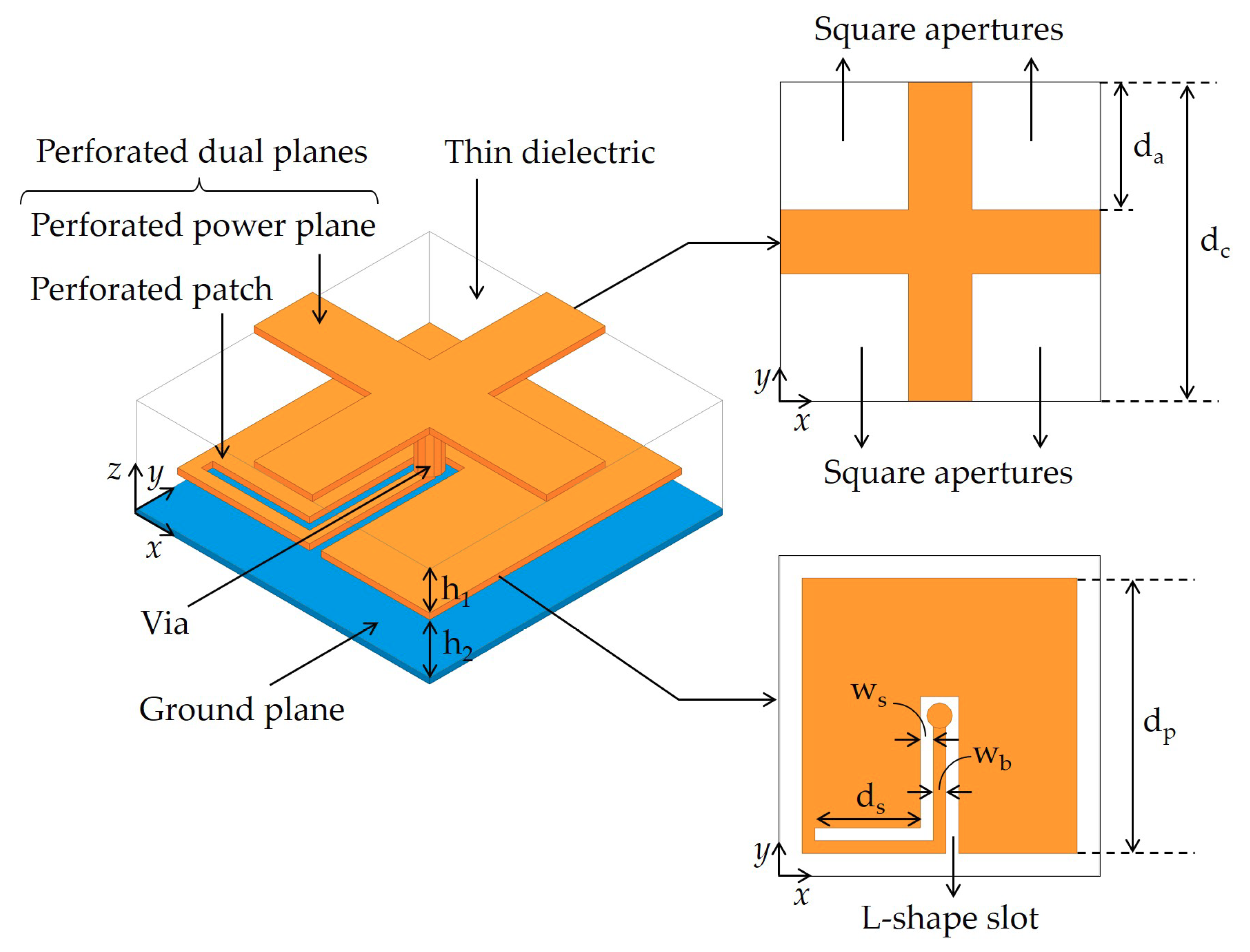
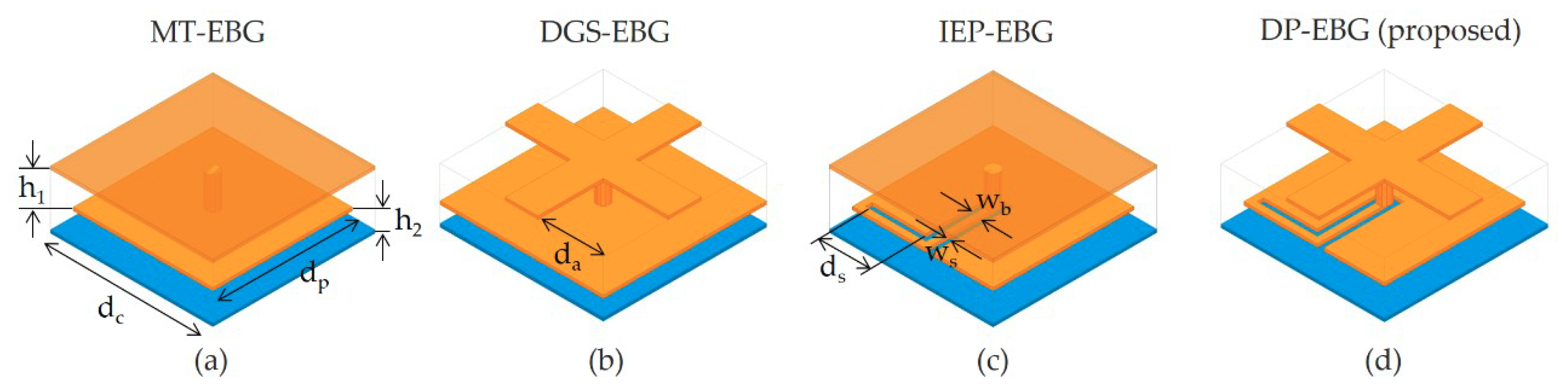
2. Dual-Perforation EBG Structure

2.1. Design Description

The proposed dual-perforation EBG (DP–EBG) structure is developed to suppress parallel-plate noise in multilayer PCBs, including thin dielectrics. The DP–EBG structure is a periodic structure in which a unit cell comprises a perforated power plane, a perforated patch, and a ground plane embedded in a thin dielectric, as shown in Figure 1. The power plane is perforated by four square apertures, while the resonant patch is perforated by an L-shape slot. These perforations are simple to implement with conventional PCB manufacturing techniques without requiring additional, costly processes. The perforated power plane and patch are connected through a short-length via owing to the thin dielectric. The apertures in the power plane electrically enhance the characteristic impedance of the EBG unit cell, while the L-shape slot in the resonant patch effectively increases the inductance of the EBG unit cell. The unit cell size and square aperture of the DP–EBG structure are represented as dc–by–dc and da–by–da structures, respectively. Therefore, the width of the remaining conductor is the same and equal to dc-2da. Regarding the L-shape slot, the conductor width etched on the patch is denoted by ws and the width of the remaining conductor is denoted by wb. The sum of dp/2 and ds is the total length of the L-shape slot. The design parameter ds is adjustable to obtain a desired patch inductance. The dielectric thickness between the dual perforated planes is h1. The distance between the perforated patch and the ground plane is h2.

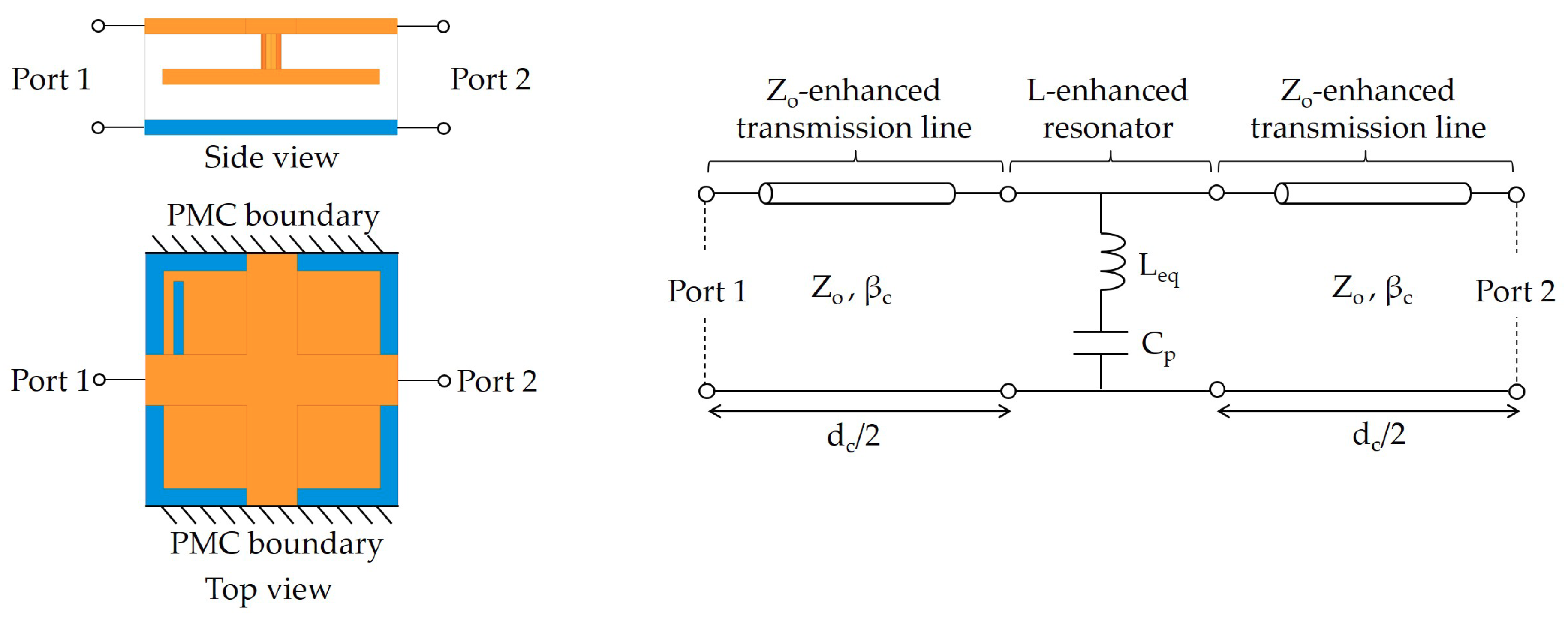
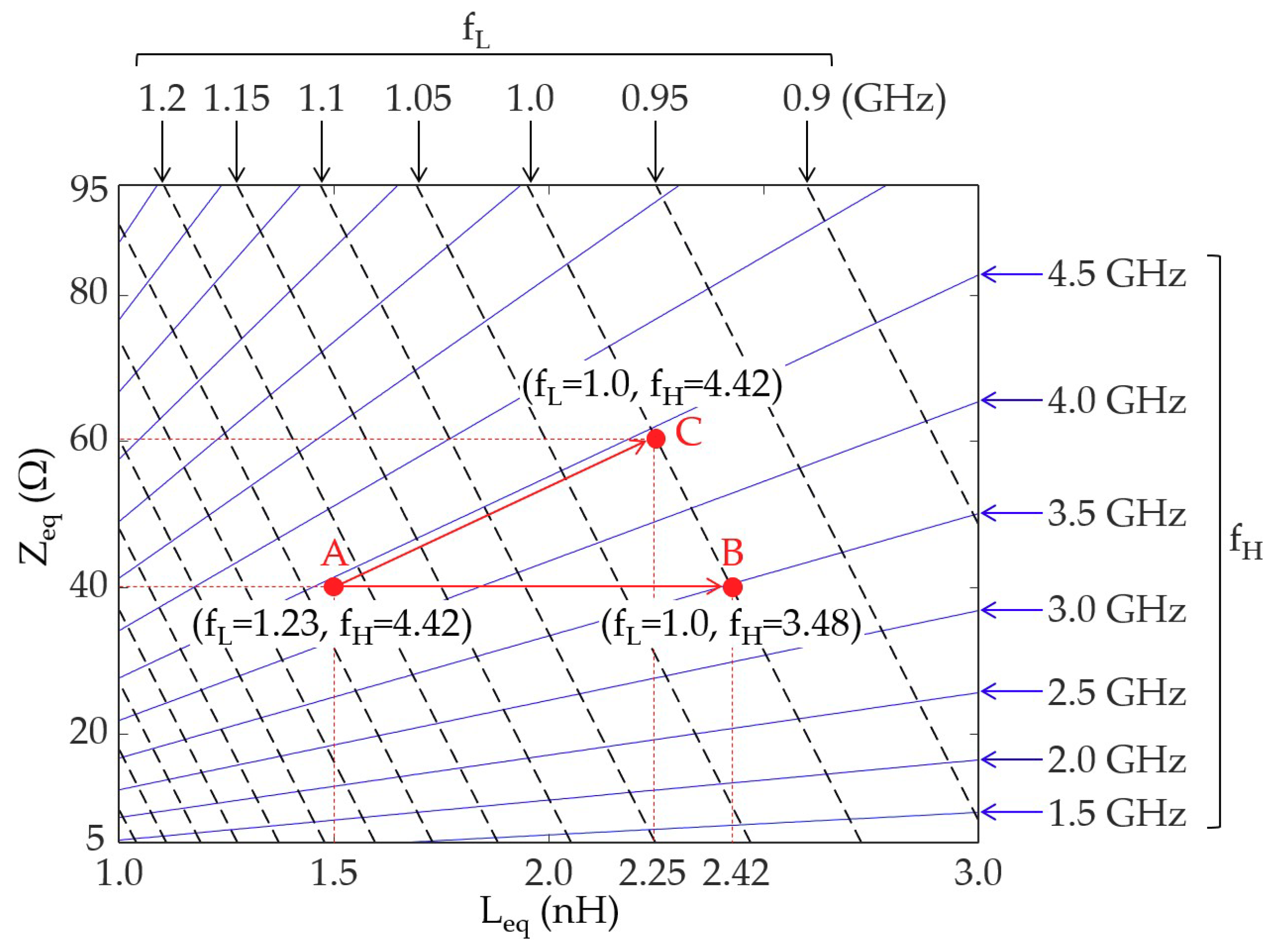
2.2. Derivation of the Equations for fL and fH

Dispersion analysis is performed to examine the dual-perforation effects on the stopband of the DP–EBG structure. To derive an analytical dispersion equation, a two-port equivalent circuit model based on transmission line theory is considered, as shown in Figure 2. In this study, one-dimensional (1–D) propagation is captured by the equivalent circuit. The dispersion analysis conducted with the use of the 1–D circuit model can be extended to a 2–D EBG array because it shows good correlation with the prediction of noise suppression in the 2–D EBG array. The DP–EBG circuit model consists of two transmission lines and a resonator circuit in which an inductor and a capacitor are connected in series. At the resonant frequency, the LC resonator has zero impedance which results in the decoupling of parallel-plate noise. The transmission line is the circuital representation of electromagnetic waves propagating through the parallel plate waveguide, which is formed by the perforated power and the ground planes. In the DP–EBG circuit model, Zeq and βc respectively denote the characteristic impedance and propagation constant of this parallel plate waveguide or transmission line. Its length is dc/2. In the transmission line model, Zeq is significantly enhanced by the square perforation aperture because the width of the remaining conductor perpendicular to the direction of wave propagation is narrowed. In the resonator circuit, the capacitance Cp is attributed to the capacitor between the resonant patch and the corresponding ground plane, while the inductance is attributed to the patch and the via inductances. For the DP–EBG structure in the thin PCBs, the inductance of the via can be ignored compared to the patch inductance which substantially increases due to the L-shape slot. Thus, the value of Leq in the DP–EBG circuit model is mainly determined by the L-shape slot on the perforated resonant patch. Hence, the equivalent circuit of the proposed DP–EBG structure is expressed with a Zo-enhanced transmission line and an L-enhanced resonator.
Using the ABCD parameters of the microwave theory, the voltage/current relationships between ports 1 and 2 of the DP–EBG unit cell are described by [22]
( cos ( β u c d c ) j Z u c sin ( β u c d c ) j Z u c 1 sin ( β u c d c ) cos ( β u c d c ) ) = ( cos ( β c d c 2 ) j Z e q sin ( β c d c 2 ) j Z e q 1 sin ( β c d c 2 ) cos ( β c d c 2 ) ) ( 1 0 Y R 1 ) ( cos ( β c d c 2 ) j Z e q sin ( β c d c 2 ) j Z e q 1 sin ( β c d c 2 ) cos ( β c d c 2 ) )
where,
Y R = j ( 2 π f ) C p 1 ( 2 π f ) 2 L e q C p
From the equations listed above, an effective phase constant βuc of the DP–EBG unit cell is derived by
β u c = 1 d c cos 1 [ cos ( β c d c ) ( 2 π f ) C p Z e q 2 ( 1 ( 2 π f ) 2 C p L e q ) sin ( β c d c ) ] .
Closed-form expressions for low and high-cutoff frequencies (fL and fH) are further extracted from (3). To derive a closed-form expression for fL, it is considered that the real part of βuc is equal to π/dc (i.e., Re{ βuc } = π/dc ). It is assumed that the electrical length of βcdc for fL is small enough to set cos(βcdc) and sin(βcdc) to 1 and βcdc, respectively. Accordingly, the following equation is obtained from (3),
1 = ( π f L C p Z e q 2 ( 1 ( 2 π f L ) 2 C p L e q ) ) ( 2 π f L d c v p ) .
where vp is the phase velocity of c / ε r , and c is the speed of light in vacuum. Based on Equation (4), an analytical equation can be derived explicitly for fL, as follows,
f L = 1 2 π ( 1 4 Z e q C p d c v p 1 + L e q C p ) 1 / 2
As it can be observed in Equation (5), fL is expected to be reduced when Zeq and Leq increase, when the DP technique is used, which are associated with the perforations of a power plane and a resonant patch. Leq mainly contributes to the reduction in fL, while the Zeq effect is limited because it is divided by the phase velocity vp.
To obtain an explicit expression for fH, it is considered that βucdc = 0 or cos(βucdc) = 1. Thus, Equation (3) may be simplified to
t a n ( β c d c 2 ) = ( 2 π f H ) C p Z e q 2 ( 1 ( 2 π f H ) 2 C p L e q )
Accordingly, Equation (6) can be approximated using two assumptions. First, dc is so small compared to the wavelength of fH which results in tan(βcdc/2) ≈ βcdc/2.
Second, fH is higher than the resonant frequency determined by the CpLeq product. Thus, (1-(2πfH)2CpLeq) is approximated to be equal to -(2πfH)2CpLeq. Consequently, (6) becomes
f H = 1 2 π ( Z e q L e q v p d c ) 1 / 2
It is observed in Equation (7) that fH can be shifted to lower the frequency values by increasing Leq with the resonant patch perforated by the L-shape slot. Considering the factor Leq in Equations (6) and (7), the fH reduction rate is higher than that of fL because fH is inversely proportional to (Leq)1/2. However, increasing Zeq, induced from the power plane perforated using rectangular apertures, compensates this bandwidth reduction in the proposed DP–EBG structure.

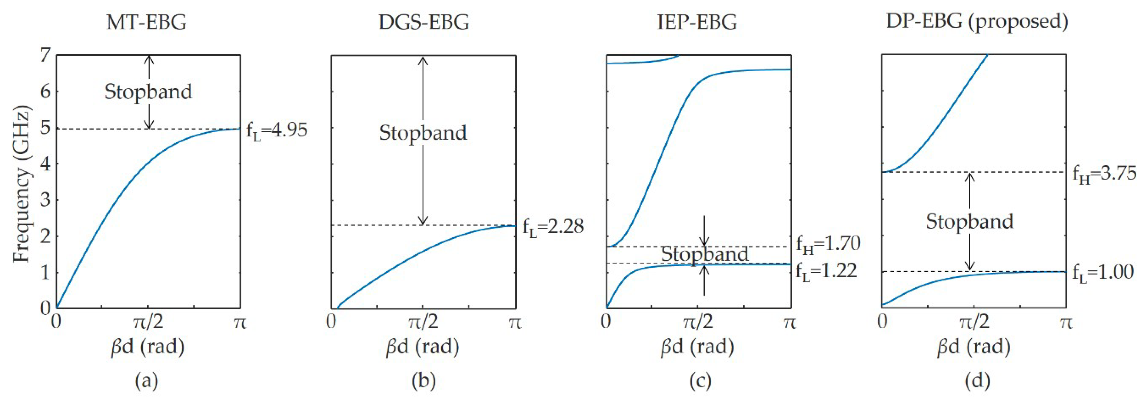
2.3. Dispersion Analysis

To validate the fL and fH equations and examine the DP technique effects on the stopband characteristics of the DP–EBG structure, a full-wave simulation based on a finite element method (FEM) is adopted, and the results are compared with those from Equations (5) and (7). FEM simulations were performed using the commercial software HFSS (ver. 17.1, Ansys. Corp., Pittsburgh, PA, USA). The FEM simulation model used for the dispersion analysis of the DP–EBG structure is identical to the unit cell shown in Figure 1. In the simulation model, the nominal values of the design parameters of dc, dp, da, ws, wb, ds, h1, and h2, are set to 5 mm, 4.9 mm, 2.45 mm, 0.1 mm, 0.1 mm, 2.2 mm, 0.1 mm, and 0.1 mm, respectively. These values were determined based on the consideration of a conventional and low-cost PCB process. The dimensions of the geometrical parameters are summarized in Table 1. The dielectric thicknesses of h1 and h2 are chosen as the minimum value provided by the cost-effective PCB process. The dielectric constant and loss tangent of the FR–4 are 4.4 and 0.02, respectively. The aperture size da and the L-shape slot length ds are respectively related with Zeq and Leq. The parameters da and ds were varied to comprehensively examine the stopband characteristics of the DP–EBG structure and to verify the closed-form expressions for fL and fH of Equations (5) and (7). The da values of 2.15, 2.25, 2.35, and 2.45 mm, are employed which correspond to the Zeq values of 33, 41, 56, and 90 Ω. The ds values changed from 0.15 mm to 2.3 mm and coincided with the Leq values from 1.55 nH to 2.38 nH. The Zeq and Leq values associated with the geometrical dimensions were simply obtained using quasistatic simulations.
Figure 3 depicts the fL and fH values of the stopband characteristics with the aforementioned Zeq and Leq values, as acquired from the FEM simulations (blue lines) and the proposed equations (red lines). The results for Zeq of 33, 41, 56, and 90 Ω, are shown in Figure 3a–d, respectively. The closed-form expressions for fL and fH exhibit good correlations with the FEM-based full-wave simulations, as shown in all the figures. The discrepancies associated with fH may result from the first-order approximation of the Taylor series expansion of the tangent function. However, the differences between the FEM simulation and the closed-form expressions are approximately uniform for all the Leq values. Thus, the tendencies among these results are in close agreement. Even though the closed-form expressions for fL and fH derived herein are verified using a limited number of test cases, these equations can be extended and applied to other DP–EBG structures, including the different dimensions of geometrical parameters.
The effects of the DP technique on a stopband are further examined. The fL and fH variations with respect to Zeq and Leq are explored using Equations (5) and (7), as shown in Figure 4. The value of Zeq varies from 5 Ω to 95 Ω and that of Leq changes from 1.0 nH to 3.0 nH. These values are commonly used for the proposed DP–EBG structure in low-cost and thin PCBs. The overall tendencies of the variations of fL and fH associated with the DP technique are also observed and evaluated. In Figure 4a, the minimum fL value is 0.85 GHz when Zeq and Leq are 95 Ω and 3.0 nH, respectively. The maximum value of fL is 1.63 GHz and results from Zeq = 5 Ω and Leq = 1.0 nH. As shown in Figure 4b, the minimum value of fH is 1.10 GHz and is observed when Zeq = 5 Ω and Leq = 3.0 nH, while the DP–EBG structure has a maximum value of fH is 8.34 GHz when Zeq = 95 Ω and Leq = 1.0 nH. The conditions for the minimum and maximum fL and fH values are different.
To gain insight into the efficient design of the DP–EBG structure, the variations of fL and fH are presented graphically. Figure 5 depicts the contour lines of both fL (black dashed lines) and fH (blue solid lines) when Zeq changes from 5 Ω to 95 Ω and when Leq changes from 1.0 nH to 3.0 nH. Point A in Figure 5 shows that fL and fH are equal to 1.23 GHz and 4.42 GHz when Zeq and Leq are 40 Ω and 1.5 nH, respectively. However, the suppression region of the parallel-plate noise given at point A needs to be extended in the low-frequency range. To achieve this, Leq can increase. For instance, fL changes from 1.23 GHz to 1.0 GHz as Leq increases from 1.5 nH (point A) to 2.42 nH (point B) by maintaining Zeq to 40 Ω. In this approach, both fL and fH are lowered, thus reducing the stopband bandwidth. To compensate for this drawback, other approaches can be considered, namely, by moving point A to C. Zeq increases from 40 Ω to 60 Ω and Leq increases from 1.5 nH to 2.42 nH, thus resulting in an fL value of 1.0 GHz and an fH value of 4.42 GHz. The fL reduction is successfully achieved by maintaining fH to 4.42 GHz. Consequently, the suppression region of the parallel plate noise is broadened as is fL is reduced. As it has been observed in the proposed analysis, the contour plots, which were extracted with the use of the closed-form expressions for fL and fH, provided a simple and systematic approach to design the DP–EBG structure in thin and cost-effective PCBs.

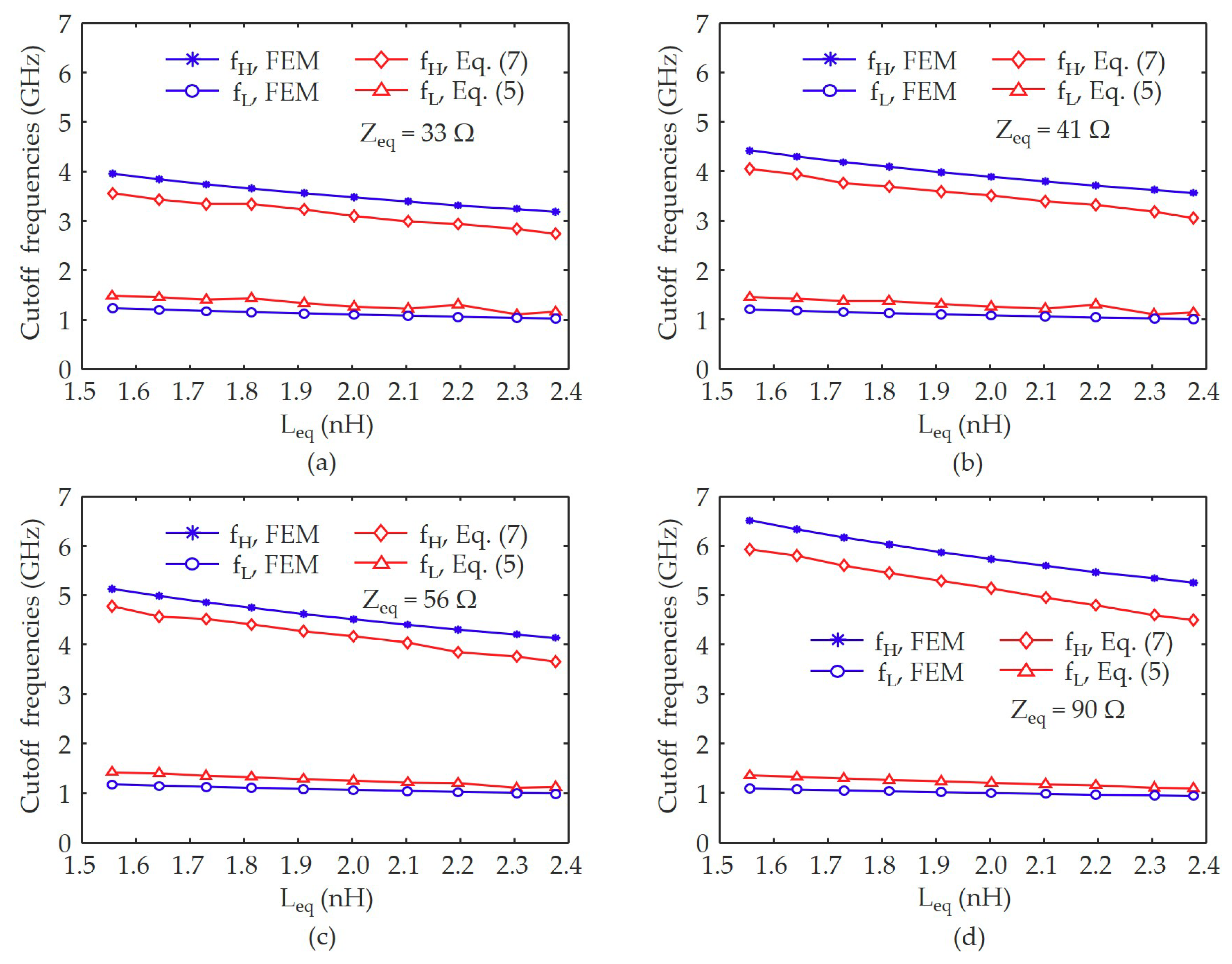
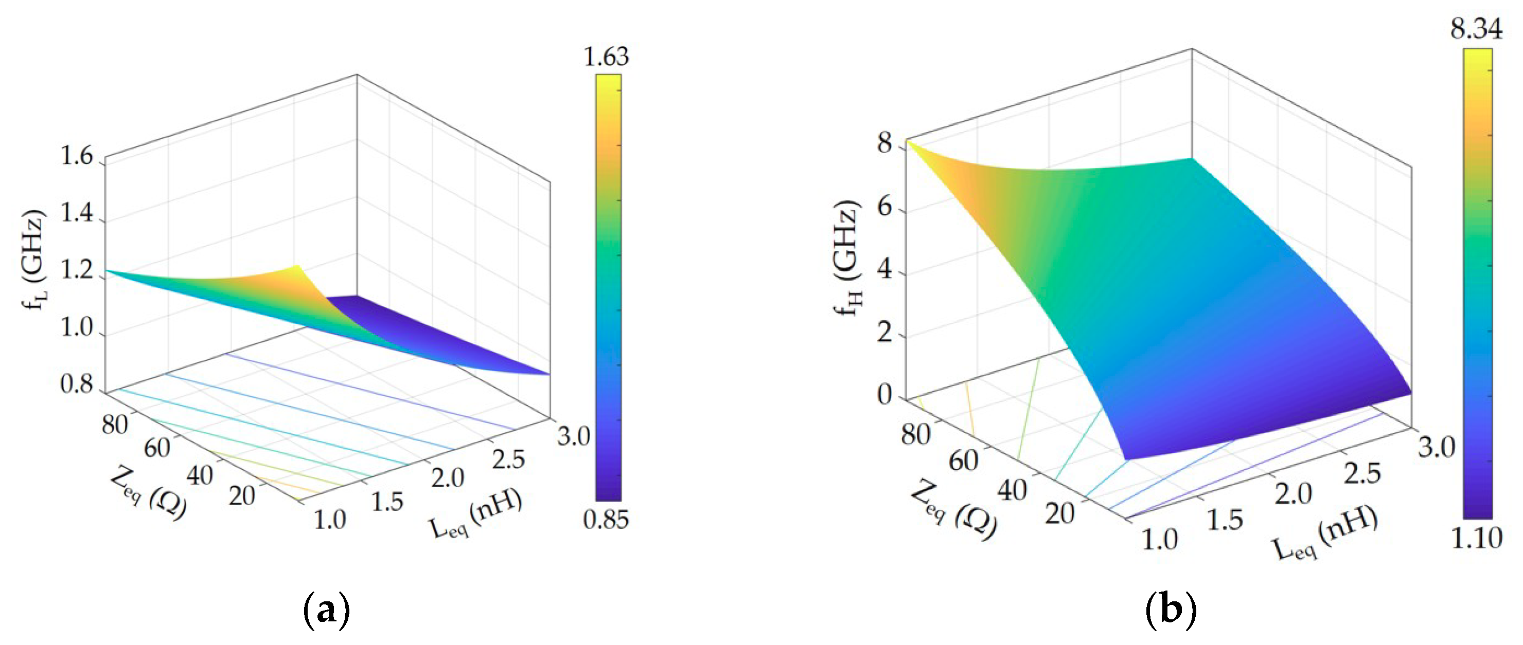
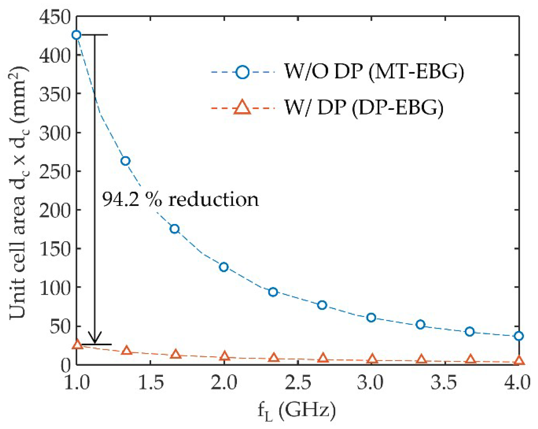
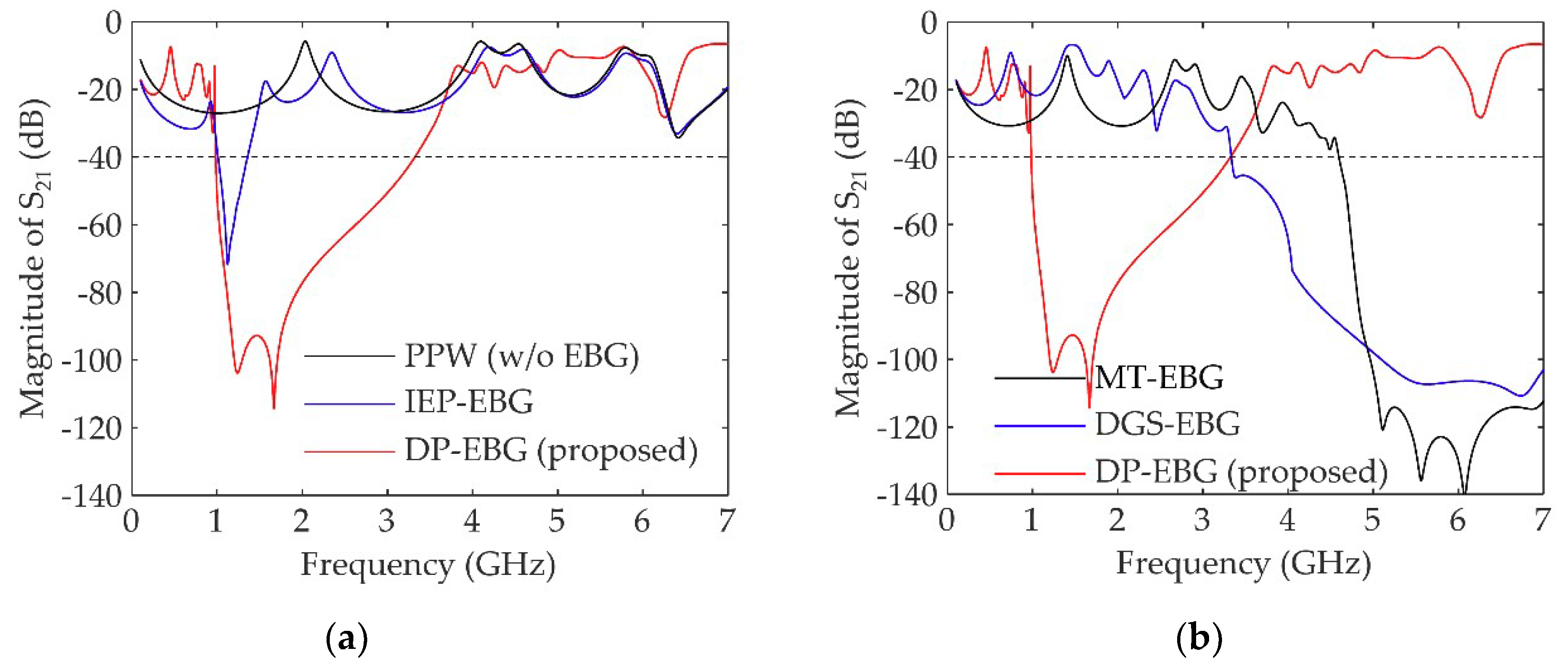
2.4. Performance Comparisons

The performances of the proposed DP–EBG structure are demonstrated by comparing their dispersion characteristics with those of previous EBG structures, namely a mushroom-type EBG (MT–EBG), defected-ground EBG (DGS–EBG), and inductance-enhanced EBG (IEP–EBG) structures. The unit cells and the dimensions of these EBG structures are shown in Figure 6 and Table 1, respectively. It is noted that the unit cells of these EBG structures have the same size. The dispersion characteristics are obtained by applying the Floquet theory to full-wave simulation results [25]. The results are illustrated in Figure 7. The fL values of the previously proposed MT–EBG, DGS–EBG, IEP–EBG, and the proposed DP–EBG structures are 4.95, 2.28, 1.22, and 1.00 GHz, respectively. For the same unit cell size, the proposed DP–EBG structure shows the lowest fL in the EBG structures. Moreover, the proposed DP–EBG structure substantially reduces fL compared to the MT– and DGS–EBG structures. Even though the stopband bandwidth of the MT– and DGS–EBG structures are larger than the DP–EBG structure, the stopbands of the MT– and DGS–EBG structures are in higher frequency ranges. These ranges cannot be lowered unless their unit cell sizes are significantly enlarged. The IEP–EBG structure has a low fL value comparable to the DP–EBG structure. However, the stopband bandwidth of the IEP–EBG structure is 0.48 GHz, which is equal to at most 0.17 times the stopband bandwidth of the DP–EBG structure. The DP–EBG structure successfully overcomes the limitation of the IEP–EBG structure, thus widening the bandwidth of the stopband.
To examine the advantage of miniaturization, an FEM-based dispersion analysis is performed to compare the previous MT–EBG and the proposed DP–EBG structures. The unit cell areas are found when the MT–EBG and DP–EBG structures contain the same fL. The comparison result is depicted in Figure 8. An amount of unit cell area reduction substantially increases as the fL is lowered. For an fL value equal to 1.0 GHz, the area reduction of the DP–EBG structure is 94.2% compared to the MT–EBG structure. It is shown that the DP–EBG structure is advantageous because it downsizes the unit cell. Remarkably, this enhancement is achieved in dual-plane perforation cases only, without requiring costly materials and additional PCB processes.

3. Results

In this section, the parallel-plate noise suppression of the DP–EBG structure in thin PCBs is demonstrated based on the scattering parameters (S-parameters) which are obtained from the full-wave simulation of the DP–EBG structure with a 7 × 7 array. Moreover, it is experimentally verified that the DP–EBG structure suppresses parallel-plate noise in thin PCBs using a test vehicle fabricated with conventional PCB process.

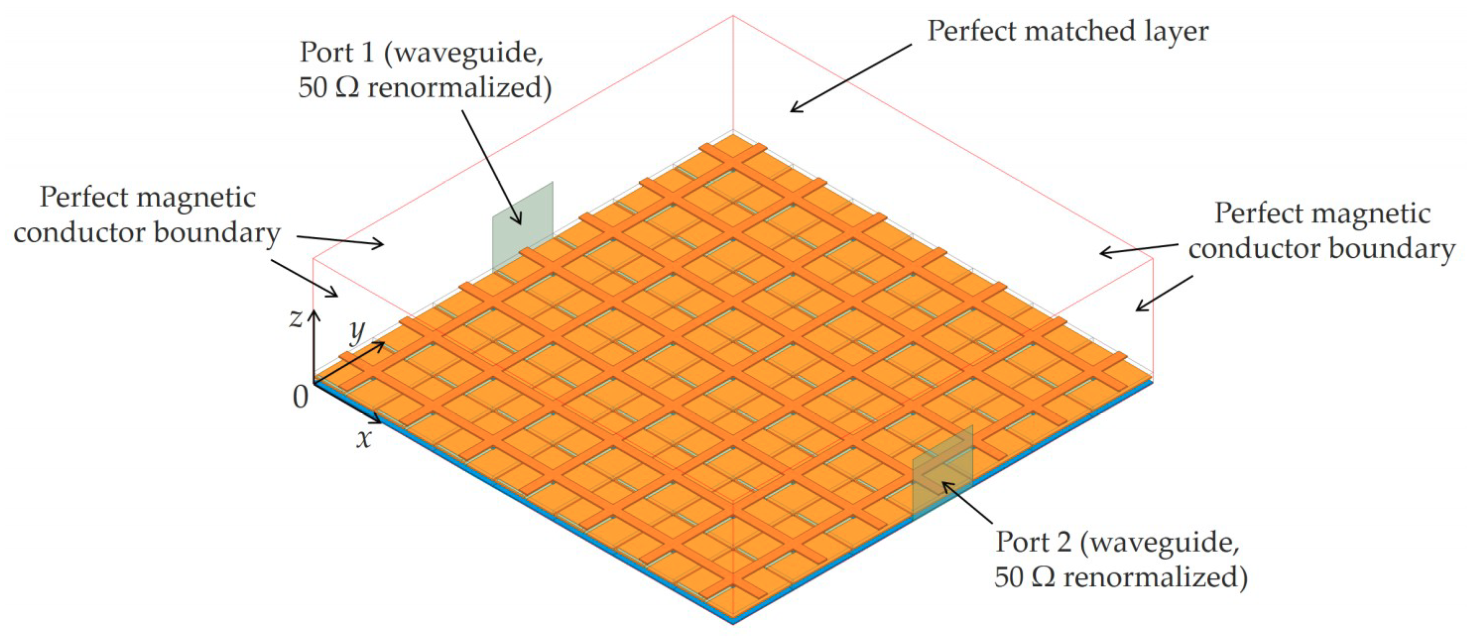
3.1. Simulated Results
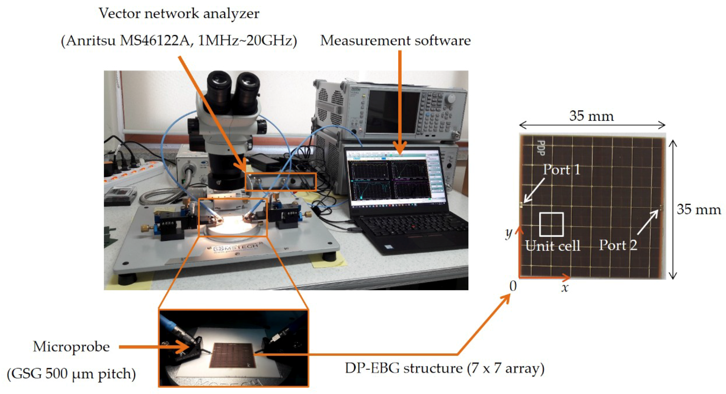
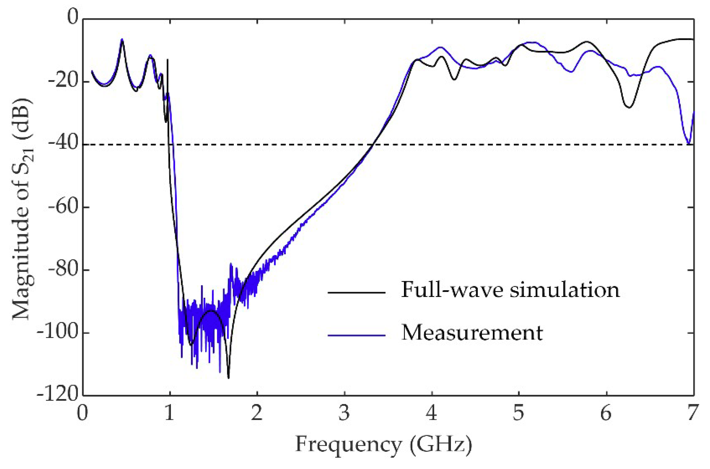
A full-wave simulation model of the DP–EBG structure with a 7 × 7 array is depicted in Figure 9. The array size is determined to implement the quasiperiodic condition of the DP–EBG structure. Two-port simulation is performed with waveguide ports renormalized to 50 Ω. The boundaries are set to perfect magnetic conductors and a perfect matched layer, as shown in Figure 9. To compare the noise suppression performance, the simulated S-parameters of the previous EBG structures with the 7 × 7 array and the parallel plate waveguide (PPW) without any EBG structure are also obtained. The dimensions of the geometrical parameters were described in the previous section. The port locations and the boundary conditions are identical for all EBG structures and the PPW.
To prove the existence of a wideband stopband with a low fL, the simulated S21 parameters of the PPW, IEP–EBG, and DP–EBG structures, are shown in Figure 10a. As it can be observed, the PPW without any EBG structure is vulnerable to parallel plate noise. The stopband with a −40 dB suppression level of the IEP–EBG structure forms in the frequency range from 1.01 GHz to 1.36 GHz, while that of the DP–EBG structure ranges from 0.98 GHz to 3.32 GHz. For the same size of the EBG structures, the stopband bandwidth of the DP–EBG structure is approximately 6.7 times wider than that of the IEP–EBG structure. Moreover, the stopband of the proposed DP–EBG structure is significantly lowered compared to those of the MT–EBG and DGS–EBG structures, as shown in Figure 10b. The fL values of the MT–EBG, DGS–EBG, and DP–EBG structures are 4.6, 3.33, and 0.98 GHz, respectively. The DP–EBG structure substantially reduces the fL value up to 78.7% without adding costly materials and processes. The stopband estimation based on the S-parameter exhibits a good correlation with dispersion analysis results. The fL and fH predicted from the dispersion analysis are 1.0 and 3.75 GHz, respectively.

3.2. Measurements

To experimentally verify the DP–EBG structure, a test vehicle is fabricated using conventional PCB process. The process provides a copper-based conduction layer, FR–4 dielectric, through-hole via, and a minimum dielectric thickness of 100 μm. The via diameter is 0.4 mm and the copper thickness is 17 μm. The dielectric constant and loss tangent of the FR–4 are 4.4 and 0.02, respectively. The dimensions for the test vehicle of the DP–EBG structure are listed in Table 1. The test vehicle includes a 7 × 7 array and the entire board size is 35 mm x 35 mm. The measurement setup and fabricated PCBs of the DP–EBG structure are depicted in Figure 11. To obtain the S-parameters of the DP–EBG structure, a vector network analyzer (Anritsu MS46122A, 1 MHZ to 1 GHz) and microprobes (GSG type, 500 μm pitch) are employed. The probing pads on the test vehicle are located at (0 mm, 17.5 mm) and (35 mm, 17.5 mm) with the origin placed at the lower left corner of the PCBs. This setup is the same as the setup of the full-wave simulation described in the previous section. The measured and simulated S21 parameters are shown in Figure 12. The stopband of the DP–EBG structure is clearly observed in the measurement. The fL and fH values with a −40 dB suppression level are equal to 1.03 and 3.32 GHz, respectively. The measurements show good agreement with the full-wave simulation result. Consequently, it is experimentally verified that the DP–EBG structure substantially suppresses the parallel-plate noise with the advantage of miniaturization (in other words, low fL) in thin and low-cost PCBs.

4. Conclusions

The DP–EBG structure was proposed to improve parallel-plate noise suppression and downsize the EBG structure in multilayer PCBs with thin dielectrics. The proposed DP technique efficiently overcame the limitations of the previous EBG structure in thin and low-cost PCBs. The perforation pattern for a resonant patch lowered the start frequency of the stopband and the plane perforation improved the stopband bandwidth. The DP technique successfully achieved these without any costly materials and processes. The improved characteristics of the DP–EBG structures were thoroughly examined and validated using dispersion analysis, full-wave simulations, and experiments. In this study, the particular patterns of the rectangular aperture and L-shape slot for the DP technique are presented. Additional research studies on other patterns for the DP technique need to be conducted. It is thus anticipated that a synthesis algorithm will be developed for the various patterns planned to be tested using the DP technique.

Author Contributions

The author conceived and designed the experiments, analyzed the characteristics, performed the simulations and experiments, and wrote the paper.

Funding

This work was supported by the National Research Foundation of Korea (NRF) grant funded by the Korea government (Ministry of Science and ICT) (NRF-2019R1C1C1005777).

Conflicts of Interest

The author declares no conflict of interest.

Abbreviations

DGSdefected ground structure
DPdual perforation
EBGelectromagnetic bandgap
FEMfinite difference method
IEPinductance-enhanced patch
MTmushroom-type
PCBprinted circuit board
PPWparallel plate waveguide

References

  1. Novak, I. Lossy power distribution networks with thin dielectric layers and/or thin conductive layers. IEEE Trans. Adv. Packag. 2000, 23, 353–360. [Google Scholar] [CrossRef]
  2. Senthinathan, R.; Prince, J.L. Simultaneous switching ground noise calculation for packaged CMOS devices. IEEE J. Solid-State Circuits 1991, 26, 1724–1728. [Google Scholar] [CrossRef]
  3. McCredie, B.D.; Becker, W.D. Modeling, measurement, and simulation of simultaneous switching noise. IEEE Trans. Compon. Packag. Manuf. Technol. Part B 1996, 19, 461–472. [Google Scholar] [CrossRef]
  4. Chun, S.; Swaminathan, M.; Smith, L.D.; Srinivasan, J.; Jin, Z.; Iyer, M.K. Modeling of simultaneous switching noise in high speed systems. IEEE Trans. Adv. Packag. 2001, 24, 132–142. [Google Scholar] [CrossRef]
  5. Tang, K.T.; Friedman, E.G. Simultaneous switching noise in on-chip CMOS power distribution networks. IEEE Trans. Very Larg. Scale Integr. Syst. 2002, 10, 487–493. [Google Scholar] [CrossRef]
  6. Swaminathan, M.; Chung, D.; Grivet-Talocia, S.; Bharath, K.; Laddha, V.; Xie, J. Designing and Modeling for Power Integrity. IEEE Trans. Electromagn. Compat. 2010, 52, 288–310. [Google Scholar] [CrossRef] [Green Version]
  7. Kamgaing, T.; Ramahi, O.M. A novel power plane with integrated simultaneous switching noise mitigation capability using high impedance surface. IEEE Microw. Wirel. Compon. Lett. 2003, 13, 21–23. [Google Scholar] [CrossRef]
  8. Abhari, R.; Eleftheriades, G.V. Metallo-dielectric electromagnetic bandgap structures for suppression and isolation of the parallel-plate noise in high-speed circuits. IEEE Trans. Microw. Theory Tech. 2003, 51, 1629–1639. [Google Scholar] [CrossRef]
  9. Lee, J.; Kim, H.; Kim, J. High dielectric constant thin film EBG power/ground network for broad-band suppression of SSN and radiated emissions. IEEE Microw. Wirel. Compon. Lett. 2005, 15, 505–507. [Google Scholar]
  10. Park, J.; Lu, A.C.W.; Chua, K.M.; Wai, L.L.; Lee, J.; Kim, J. Double-stacked EBG structure for wideband suppression of simultaneous switching noise in LTCC-based SiP applications. IEEE Microw. Wirel. Compon. Lett. 2006, 16, 481–483. [Google Scholar] [CrossRef]
  11. Wang, C.D.; Yu, Y.M.; de Paulis, F.; Scogna, A.C.; Orlandi, A.; Chiou, Y.P.; Wu, T.L. Bandwidth Enhancement Based on Optimized Via Location for Multiple Vias EBG Power/Ground Planes. IEEE Trans. Compon. Packag. Manuf. Technol. 2012, 2, 332–341. [Google Scholar] [CrossRef]
  12. Rajo-Iglesias, E.; Inclan-Sanchez, L.; Vazquez-Roy, J.; Garcia-Munoz, E. Size Reduction of Mushroom-Type EBG Surfaces by Using Edge-Located Vias. IEEE Microw. Wirel. Compon. Lett. 2007, 17, 670–672. [Google Scholar] [CrossRef]
  13. Awasthi, S.; Biswas, A. Compact filter using coupled metamaterial mushroom resonators with corner vias. In Proceedings of the 2011 IEEE Applied Electromagnetics Conference (AEMC), Kolkata, India, 18–20 December 2011; pp. 1–4. [Google Scholar]
  14. Kamgaing, T.; Ramahi, O.M. Multiband Electromagnetic-Bandgap Structures for Applications in Small Form-Factor Multichip Module Packages. IEEE Trans. Microw. Theory Tech. 2008, 56, 2293–2300. [Google Scholar] [CrossRef]
  15. Kasahara, Y.; Toyao, H. Compact (lambda/45-Sized) Electromagnetic Bandgap Structures With Stacked Open-Circuit Lines. IEEE Microw. Wirel. Compon. Lett. 2017, 27, 694–696. [Google Scholar] [CrossRef]
  16. Kasahara, Y.; Toyao, H.; Hankui, E. Compact and Multiband Electromagnetic Bandgap Structures with Adjustable Bandgaps Derived From Branched Open-Circuit Lines. IEEE Trans. Microw. Theory Tech. 2017, 65, 2330–2340. [Google Scholar] [CrossRef]
  17. Shen, C.; Chen, S.; Wu, T. Compact Cascaded-Spiral-Patch EBG Structure for Broadband SSN Mitigation in WLAN Applications. IEEE Trans. Microw. Theory Tech. 2016, 64, 2740–2748. [Google Scholar] [CrossRef]
  18. Kim, M. A Miniaturized Electromagnetic Bandgap Structure Using an Inductance-Enhanced Patch for Suppression of Parallel Plate Modes in Packages and PCBs. Electronics 2018, 7, 76. [Google Scholar] [CrossRef]
  19. Zhang, M.; Li, Y.; Jia, C.; Li, L. A Power Plane with Wideband SSN Suppression Using a Multi-Via Electromagnetic Bandgap Structure. IEEE Microw. Wirel. Compon. Lett. 2007, 17, 307–309. [Google Scholar] [CrossRef]
  20. Park, H.H. Reduction of Electromagnetic Noise Coupling to Antennas in Metal-Framed Smartphones Using Ferrite Sheets and Multi-Via EBG Structures. IEEE Trans. Electromagn. Compat. 2018, 60, 394–401. [Google Scholar] [CrossRef]
  21. Han, Y.; Huynh, H.A.; Kim, S. Pinwheel Meander-Perforated Plane Structure for Mitigating Power/Ground Noise in System-in-Package. IEEE Trans. Compon. Packag. Manuf. Technol. 2018, 8, 562–569. [Google Scholar] [CrossRef]
  22. Kim, M.; Koo, K.; Hwang, C.; Shim, Y.; Kim, J.; Kim, J. A Compact and Wideband Electromagnetic Bandgap Structure Using a Defected Ground Structure for Power/Ground Noise Suppression in Multilayer Packages and PCBs. IEEE Trans. Electromagn. Compat. 2012, 54, 689–695. [Google Scholar]
  23. Kim, M.; Kam, D.G. A Wideband and Compact EBG Structure with a Circular Defected Ground Structure. IEEE Trans. Compon. Packag. Manuf. Technol. 2014, 4, 496–503. [Google Scholar] [CrossRef]
  24. Kim, Y.; Cho, J.; Cho, K.; Park, J.; Kim, S.; Kim, D.H.; Park, G.; Sitaraman, S.; Raj, P.M.; Tummala, R.R.; et al. Glass-Interposer Electromagnetic Bandgap Structure with Defected Ground Plane for Broadband Suppression of Power/Ground Noise Coupling. IEEE Trans. Compon. Packag. Manuf. Technol. 2017, 7, 1493–1505. [Google Scholar] [CrossRef]
  25. Collin, R.E. Field Theory of Guided Waves; IEEE Press: New York, NY, USA, 1990. [Google Scholar]
Figure 1. A unit cell of a dual-perforation electromagnetic bandgap dual-perforation–electromagnetic bandgap (DP–EBG) structure consisting of perforated dual planes and its design parameters.
Electronics 08 00719 g001
Figure 2. Equivalent circuit model of the DP–EBG unit cell based on transmission line theory for the extraction of the dispersion equation.
Electronics 08 00719 g002
Figure 3. Various cutoff frequencies with respect to the changes of Zeq ((a) 33 Ω, (b) 41 Ω, (c) 56 Ω and (d) 90 Ω) and Leq used to examine the stopband characteristics and verify the closed-form expressions for fL and fH.
Electronics 08 00719 g003
Figure 4. Variations of (a) fL and (b) fH for various Zeq and Leq values obtained using the closed-form expressions.
Electronics 08 00719 g004
Figure 5. Contour plots of fL and fH used for the design and analyses of DP–EBG structures.
Electronics 08 00719 g005
Figure 6. Unit cells of (a) mushroom-type (MT)–, (b) defected ground structure (DGS)–, (c) inductance-enhanced patch (IEP)–, and (d) DP–EBG structures for stopband comparisons.
Electronics 08 00719 g006
Figure 7. Dispersion diagrams of (a) MT–, (b) DGS–, (c) IEP–, and (d) DP–EBG structures.
Electronics 08 00719 g007
Figure 8. Comparison of unit-cell miniaturization between previous MT– and proposed DP–EBG structures.
Electronics 08 00719 g008
Figure 9. Finite difference method (FEM)-based simulation model of the DP–EBG structure with a 7 × 7 array.
Electronics 08 00719 g009
Figure 10. Comparison of S-parameters between (a) the ppw, IEP-EBG and proposed EBG structures and (b) MT-EBG, DGS-EBG, and proposed EBG structures to demonstrate a broad stopband bandwidth and miniaturization.
Electronics 08 00719 g010
Figure 11. Measurement setup for DP–EBG structure with a 7 × 7 array.
Electronics 08 00719 g011
Figure 12. Measured and simulated S21 parameters of the DP–EBG structure.
Electronics 08 00719 g012
Table 1. Dimensions of geometrical parameters of the DP–EBG structure.
Parametersdcdpdawswbdsh1h2
Dimensions (mm)54.92.450.10.12.20.10.1

