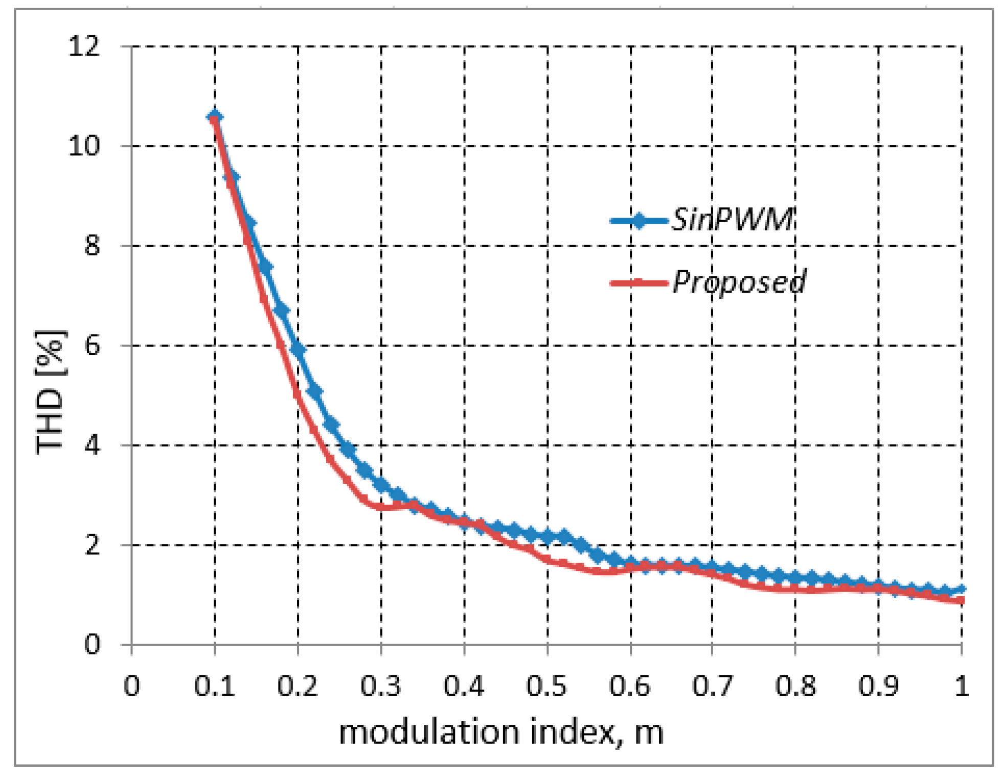
4.1. Principle of the Proposed Algorithm
The switching loss depends on the current through power switches, the voltage across the switch, and the number of commutations in the period of control voltage is shown in Equations (14)–(18). Since the switching loss can be decreased by reducing switching frequency of Sx5 and Sx4 and reducing the number of commutations on the phase, which has the absolute of the load current is high or medium in comparison to another phase. Therefore, in the first stage, the new control voltages are determined with a non-switching state on the phase, which has the smallest displacement to top or bottom peak (of the carrier) and the absolute of the load current being the first or second largest. In addition, in the second stage, the control voltages that have been determined in the previous stage, are divided into the control voltage for the two-level inverter and three-level T-type inverter for reducing switch turn-on/turn-off on the two-level inverter.
The first stage:
It is defined that
vx is the initial control voltage phase
x (
x = a, b, c) and
vrx is control voltage that it is determined as the new control voltage by adding v
offset into
vx from first stage of proposed algorithm. The maximum ampplitude of carrier is selected by 1. Due to the 5-level inverter, threshold comparison of the carrier is 0, 1, 2, 3 and 4. The initial control voltage of phase
vx is determined as Equation (19).
where
vx,
m,
ω and
θ0x are the initial control voltage of phase
x, modulation index, angular velocity, and initial phase angle, respectively.
The error of
vx and
Lx are determined:
Call
IxABS is the absolute of current across phase
x, then
where
θ is phase angle,
ILx is the load current of phase
x (
x = a, b, c).
The maximum, minimum, medium of error (
emax,
emin,
emed) and the maximum and medium of absolute of load current (
Imax,
Imed) are defined:
Case 1: When the
ixABS is the largest and (
ex =
emin) or (
ex =
emax), the none switching phase is
x and the offset voltage (
voffset) is determined through the value e
x as Equation (25)
Case 2: When
iaABS is the largest and
ea equal the
emed, for reducing error of output voltages, the offset voltage will be not equal to
ea. In this case, another phase has the absolute of the load current as medium (assuming it is phase b) and the error (
eb) of
vb and
Lb fix the maximum or minimum. Then, the offset voltage is calculated following
ibABS and
eb as Equation (26)
Thus, the offset values can be determined as
ixABS and
ex in
Table 2.
If the matrixes from Equation (27) to Equation (31) are defined, the offset voltage will be calculated as Equation (32).
The new control voltage
vrx is determined
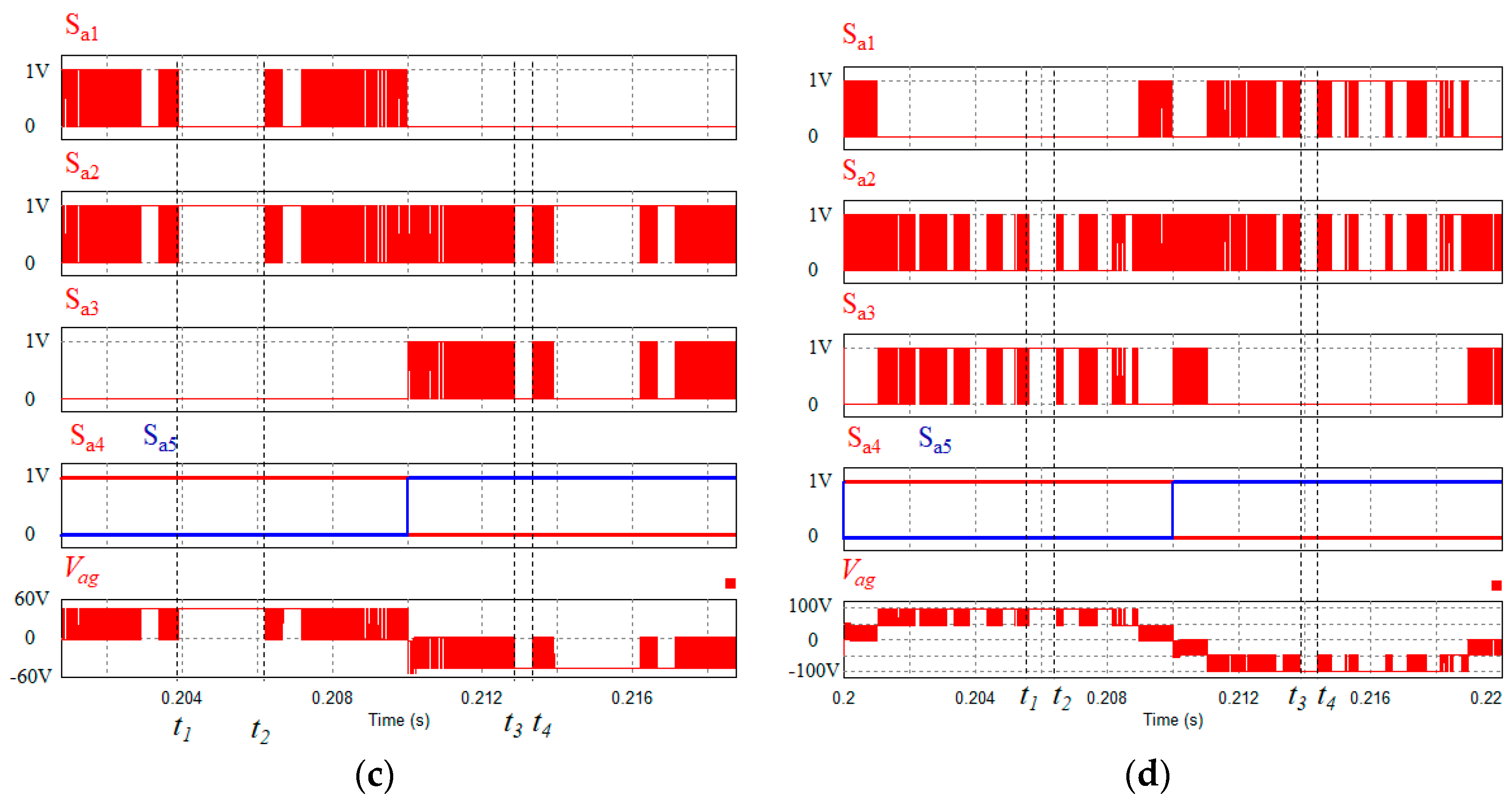
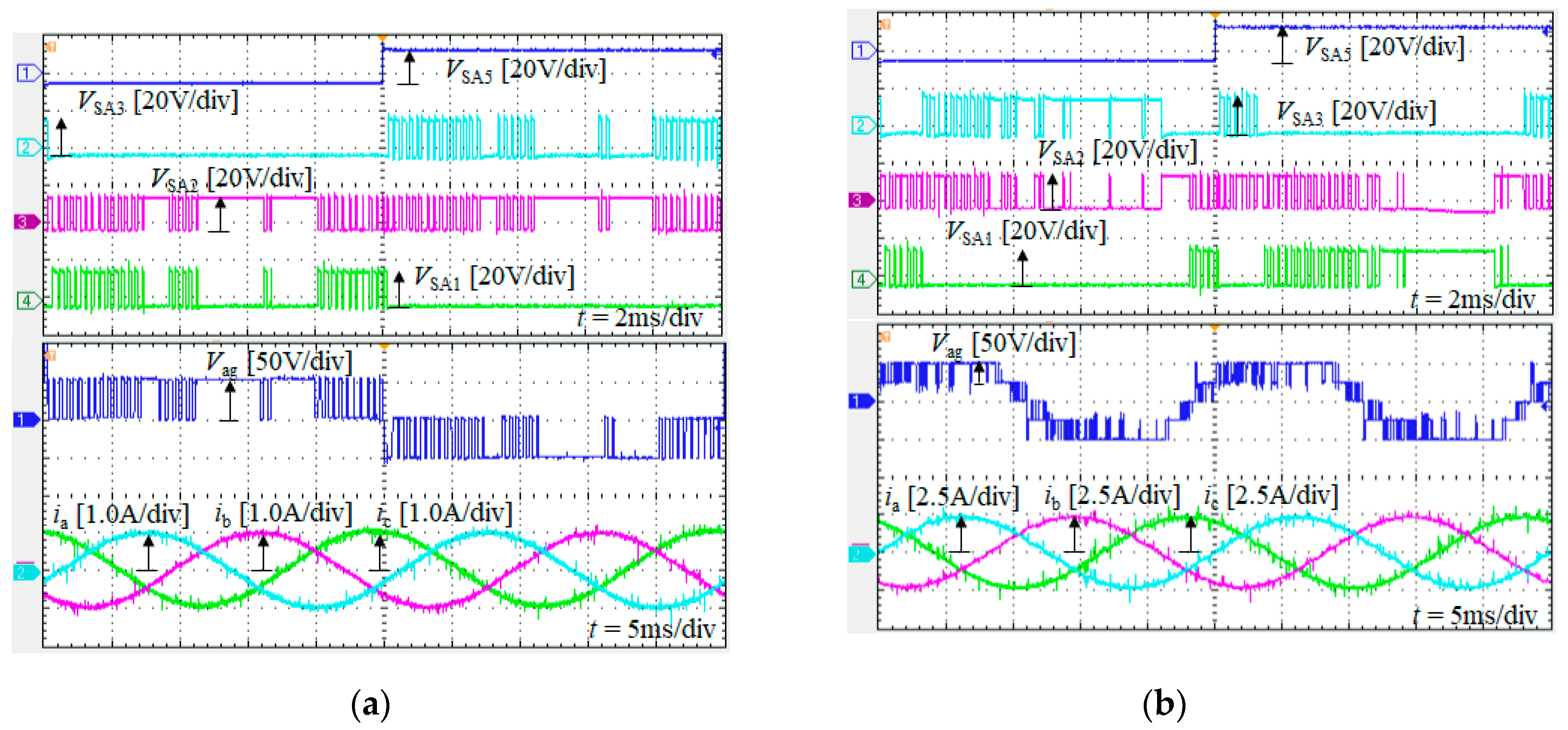
Since matrixes [], [], [], [ and [] have “0” and “1” values, which can be determined by simple comparison commands lead to the calculation of the offset voltage easy and quick. The new control voltage (vrx) is the old control voltage (vx) add the offset voltage. The new control voltages (vrx) on the phase which the absolute of the load current are first or the second large in three-phase and ex equal emax or emin will be shifted to the top or bottom peak of the carrier.
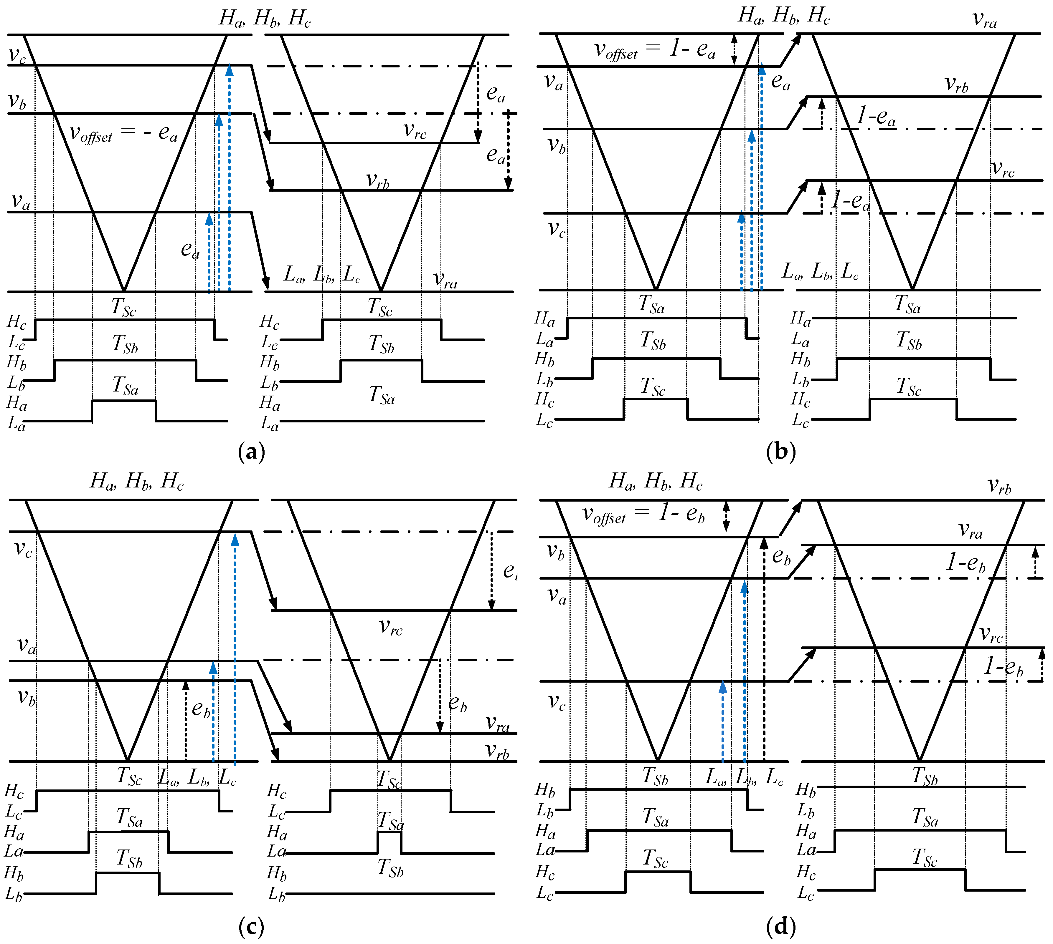
Figure 2 shows the shift of the control voltages according to the conditions of the proposed algorithm. As shown in
Figure 2a, when
, the offset voltage is
−ea. This offset voltage is added to the original control voltages so the new control voltages will shift down to the new positions. The new position of the control voltage of phase-a will be
La. Therefore, there will be no switching on the phase-a when
as shown in
Figure 2b. Similarly, the switching state on the phase-b is off if
, as shown in
Figure 2c or
Figure 2d.
The second stage:
In the second stage, the control voltages that were created in the previous stage will be divided into the control voltage for the two-level inverter and three-level T-type inverter. Since the two-level inverter is operated in six-step mode, its control voltage can be calculated as
In addition, from Equation (7), it is easy to determine the control voltages for three-level T type, which are:
where
vrx is the control voltage, created form first stage;
vx,2l and
vx,3l are the control voltages for two-level inverter and T-type inverter on phase
x.
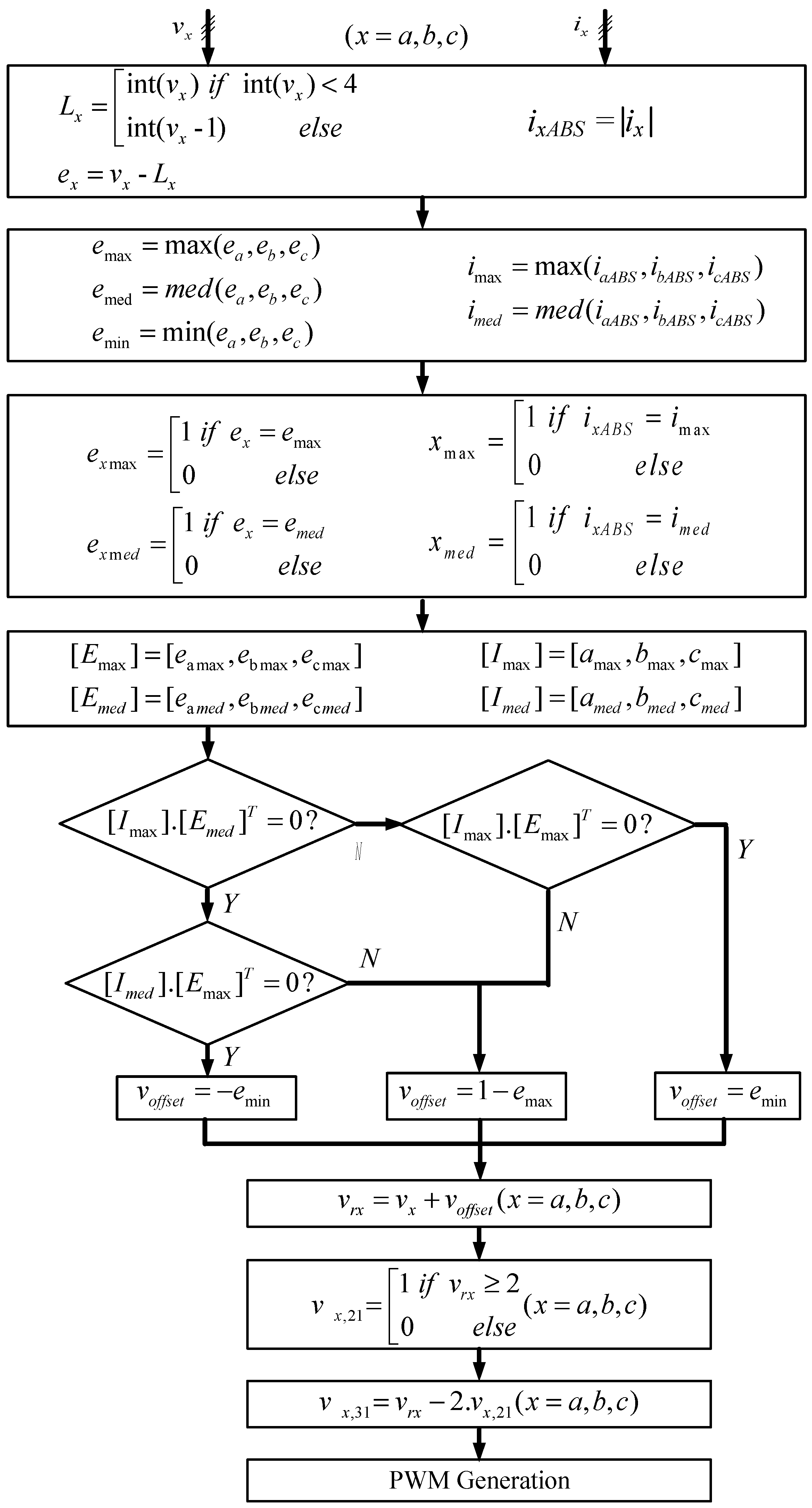
4.2. Flow Chart
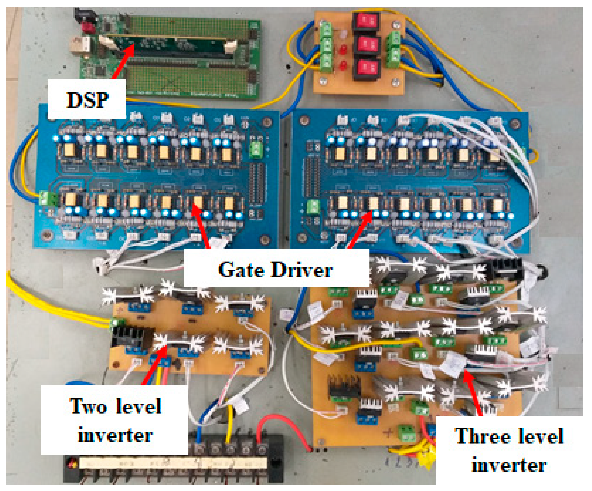
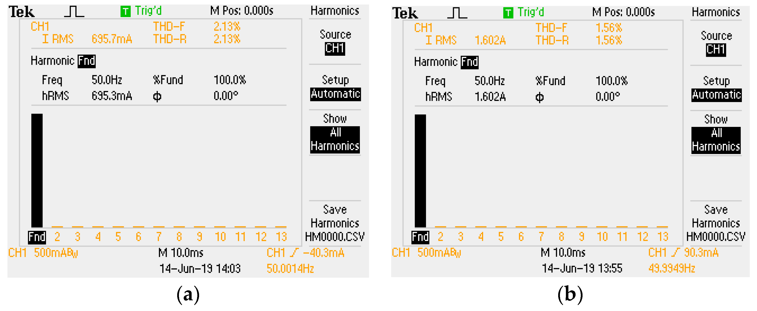
Figure 3 shows a flow chart of the proposed algorithm using simple commands such as subtraction, and comparison on the program. The comparison of the phase currents can be done by comparing hardware circuits that do not require the use of expensive sensors. Thus, calculation time of the algorithm is low and suitable for closed-loop control or other control methods.
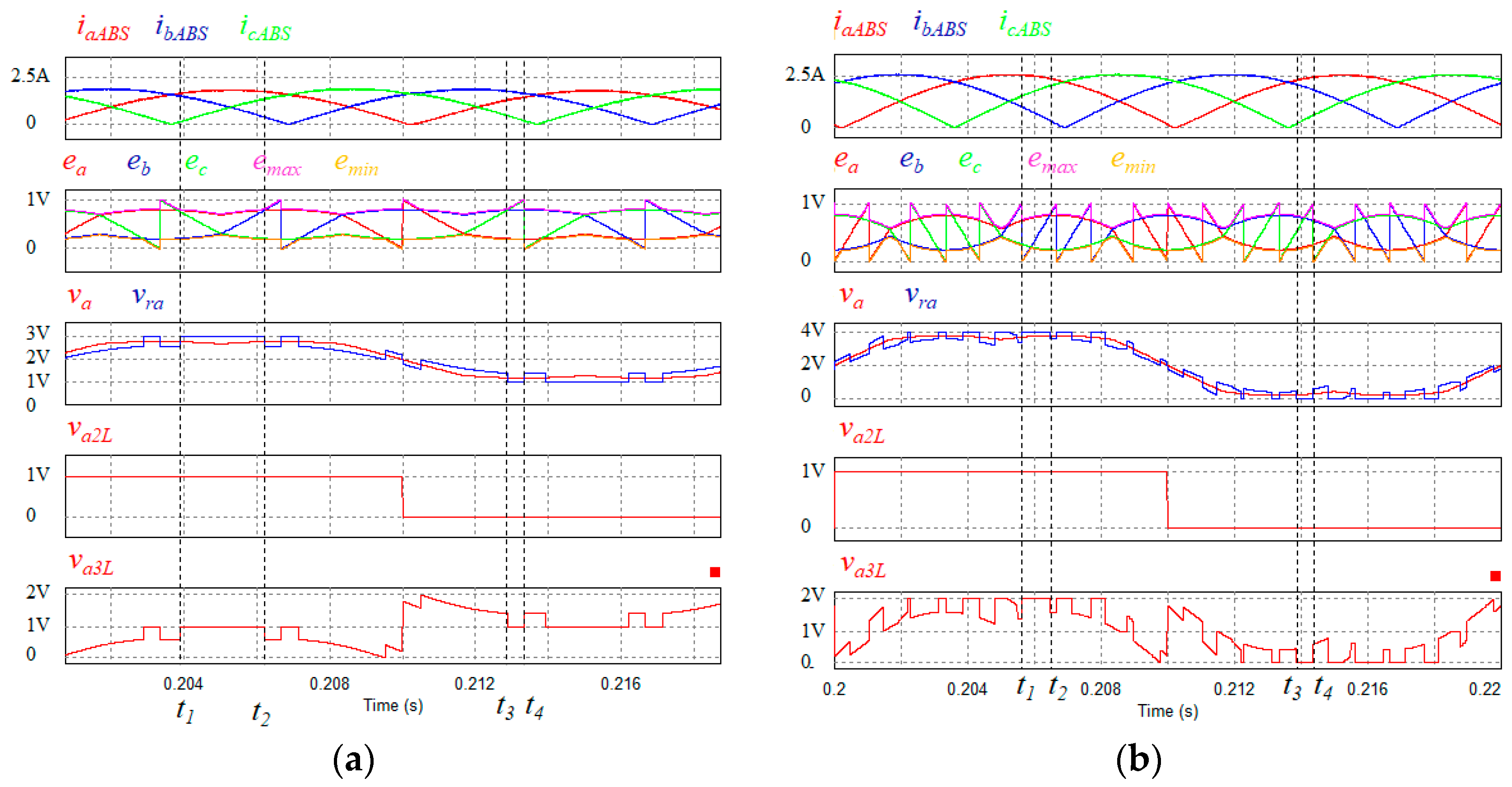
For example, assuming that control voltages va, vb, and vc are 1.12 V, 0.64 V and 3.24 V, respectively, from Equation (22), the error of vx and Lx are . From Equation (24), .
Assuming that IaABS > IbABS > IcABS, from Equations (27) and (28), . From Equations (30)–(32), . From Equations (22)–(32), the offset voltage is . Then, new control voltages are
When vra = 1 V, switches S1, S3, and S5 are turned off while switches S2 and S4 are turned on. Thus, the phase-a switches will not be switched in one cycle T. Similarly, when vrc = 3.12 V, S1, S3, and S4 are turned off while S2 and S5 are switching. As a result, the phase-c switches will be switched in one cycle T. Therefore, the proposed algorithm can reduce the switching times of the switches.


