Article

Area-Efficient Embedded Resistor-Triggered SCR with High ESD Robustness

State Key Laboratory of Electronic Thin Films and Integrated Devices, University of Electronic Science and Technology of China, Chengdu 610054, China
*
Author to whom correspondence should be addressed.
Electronics 2019, 8(4), 445; https://doi.org/10.3390/electronics8040445
Submission received: 21 March 2019 / Revised: 13 April 2019 / Accepted: 17 April 2019 / Published: 18 April 2019
(This article belongs to the Section Microelectronics)

Abstract

:
The trigger voltage of the direct-connected silicon-controlled rectifier (DCSCR) was effectively reduced for electrostatic discharge (ESD) protection. However, a deep NWELL (DNW) is required to isolate PWELL from P-type substrate (PSUB) in DCSCR, which wastes part of the layout area. An area-efficient embedded resistor-triggered silicon-controlled rectifier (ERTSCR) is proposed in this paper. As verified in a 0.3-μm CMOS process, the proposed ERTSCR exhibits lower triggering voltage due to series diode chains and embedded deep n-well resistor in the trigger path. Additionally, the proposed ERTSCR has a failure current of more than 5 A and a corresponding HBM ESD robustness of more than 8 KV. Furthermore, compared with the traditional DCSCR, to sustain the same ESD protection capability, the proposed ERTSCR will consume 10% less silicon area by fully utilizing the lateral dimension in the deep n-well extension region, while the proposed ERTSCR has a larger top metal width.

1. Introduction

The silicon-controlled rectifier (SCR) has been widely used in electrostatic discharge (ESD) protection for a long time due to its significantly high robustness and area efficiency [1]. However, the SCR device still has a higher trigger voltage, which is generally greater than the gate-oxide breakdown voltage of the protected device [2]. Thus, some modified SCR devices and trigger-assist SCR devices have been invented to reduce the trigger voltage of SCR, such as the modified lateral SCR (MLSCR) [3], the low-voltage triggering SCR (LVTSCR) [4,5], the GGNMOS-triggered SCR [6] and the diode chain triggering SCR (DTSCR) [7]. Furthermore, the direct-connected SCR (DCSCR) has been proposed to significantly reduce the trigger voltage to a level that is as low as twice of one diode’s turn-on voltage [8,9,10,11,12,13].
The cross-sectional view and equivalent circuit diagram of the conventional DCSCR are shown in Figure 1a,b. As shown in Figure 1a, the main SCR conduction path of DCSCR (illustrated by a red arrow) is triggered by two direct-connected diodes D1 (P+/NWELL diode) and D2 (PWELL/N+ diode), which are located in the adjacent NWELL and PWELL, respectively (illustrated by a blue arrow named as diode chain path). These two diodes are connected by anode gate (N+ in NWELL) and cathode gate (P+ in PWELL), which are connected together by a metal connection. Unlike the PWELL grounded in the conventional lateral SCR structure, the PWELL in DCSCR is not grounded and thus, a deep NWELL (DNW) is required to isolate PWELL from the P-type substrate (PSUB) [9]. Generally, the minimum extension (L1) of a DNW region beyond a PWELL region is several micrometers according to the layout design rule, which will result in the DCSCR consuming more silicon area compared to the conventional SCR. To optimize the layout area of DCSCR, an embedded resistor-triggered silicon-controlled rectifier (ERTSCR) is presented in this work. Compared to the conventional DCSCR with a figure of merit (FOM) of 3.30 mA/μm2, the FOM of proposed ERTSCR is 3.66 mA/μm2, which is higher by 10.9% compared to that of the conventional DCSCR. Additionally, the proposed ERTSCR has more robustness and a uniform metal connection against the huge ESD current.

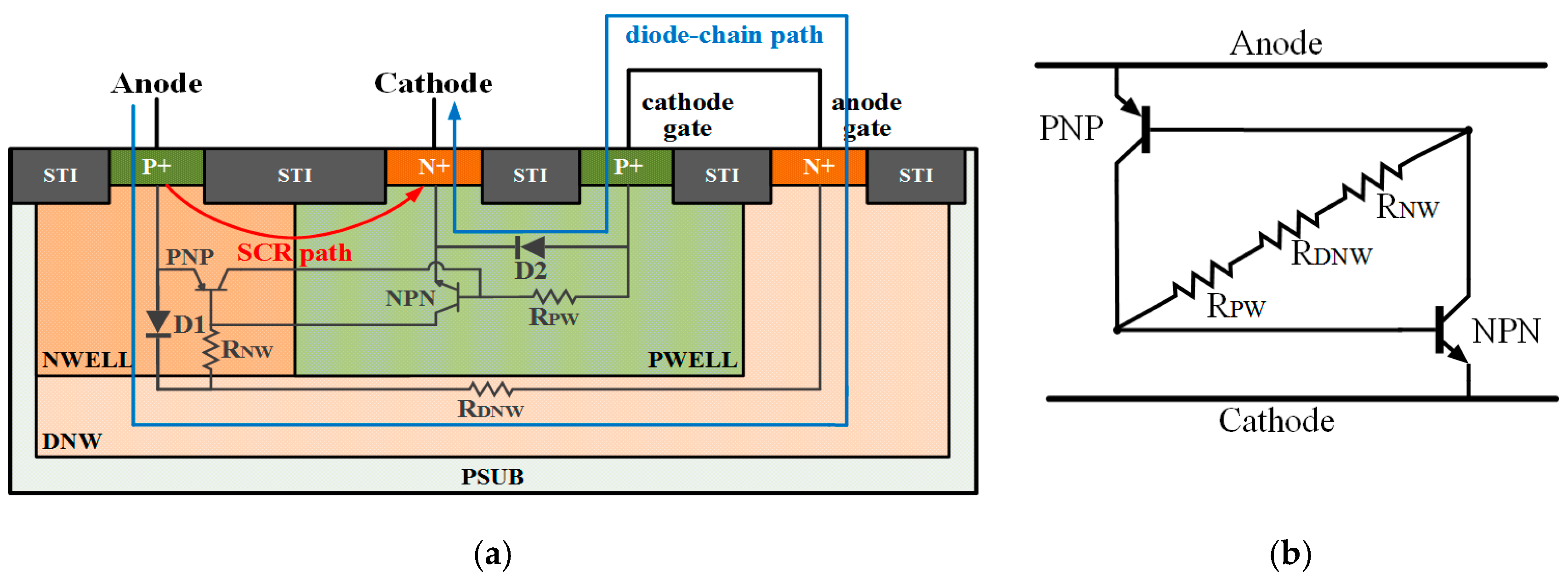
2. Proposed ESD Device Structure and Simulation

In the conventional DCSCR, the DNW cannot be fully utilized although it has a sufficient width of L1. Actually, the DNW has the same doping type as NWELL and thus, it can be regarded as an embedded deep well resistor (RDNW), which conduct the surface of DNW region and the NWELL region. Therefore, the N+ active region of the anode gate in the NWELL region can be moved to the surface of DNW region, which will not affect the turning on of D1 and D2. By making use of the conductive DNW, an area-efficient ERTSCR is proposed in this paper. The cross-sectional view and equivalent circuit diagram of proposed ERTSCR are shown in Figure 2a,b. It can be observed that the anode gate in ERTSCR is moved from NWELL to DNW and is connected to the cathode gate in adjacent PWELL by a metal connection. Compared with the DCSCR structure shown in Figure 1a, the lateral dimension of NWELL in ERTSCR will decrease due to the removal of anode gate, while the lateral dimension of DNW is unchanged. Correspondingly, the layout area of ERTSCR is smaller than that of DCSCR, which leads to a smaller layout area cost. From above, the use of RDNW can reduce the device layout area. In the meantime, RDNW plays an important role in the trigger path. Compared with DCSCR, the diode chain path in ERTSCR has one more RDNW in series with D1 and D2. However, RDNW is a conductor in trigger path and thus, the triggering of ERTSCR is still mainly determined by the turning on of two embedded diodes D1 and D2, which is similar to DCSCR.
In order to further explore the physics mechanisms of the DCSCR and proposed ERTSCR, a two dimension (2D) Technology Computer-Aided Design (TCAD) simulation was carried out using the Sentaurus tool, where the substrate of the device was regarded as the only heat sink and the ambient temperature was set at 300 K. The current density distributions in the triggering procedures of the DCSCR and proposed ERTSCR are shown in Figure 3 and Figure 4. When the ESD pulse that is applied to the anode of both DCSCR and ERTSCR is more than two times one diode’s turn-on voltage, D1 and D2 turn on and the trigger current flows through the diode chain path of each device (as shown in Figure 3a and Figure 4a). As a result, the parasitic lateral NPN transistor and PNP transistor turn on (as shown in Figure 3b and Figure 4b). As the current continues to increase, the current gain of the parasitic NPN transistor (βNPN) and the current gain of the PNP transistor (βPNP) will increase. Consequently, this gives rise to the regeneration between the two parasitic NPN and PNP transistors and thus, SCR paths are triggered (as shown in Figure 3c and Figure 4c). Finally, the SCR paths of both DCSCR and ERTSCR discharge more current than the parallel diode chain paths due to the smaller turn-on resistance (as shown in Figure 3d and Figure 4d). Compared to the current density distributions in DCSCR, the current density distributions in ERTSCR indicate that the DNW acts as an electrical connection between D1 and D2 to conduct the trigger current.

3. Layout Design of Proposed ERTSCR

The proposed ERTSCR has been fabricated together with a conventional DCSCR in a 0.3-μm CMOS process. Figure 5a,b illustrate the layout top views of the conventional DCSCR and proposed ERTSCR with the same device width of 75 μm. In accordance with the design rule of this 0.3-μm CMOS process, the conventional DCSCR has a device length of 21.4 μm, while the proposed ERTSCR has a device length of 19.3 μm, with an area reduction of approximately 10% compared with the DCSCR as illustrated by the yellow rectangle in Figure 5a.
For SCR type devices with a smaller turn-on resistance and highest ESD current conduction capability per unit, the robustness of metal connection from the PADs to the anode and cathode of SCR device will be critical in the development of an optimized ESD discharging structure [14,15,16]. Regarding the conventional DCSCR structure, as shown in Figure 5a, the metal connections of PADs and anode/cathode have been split into six metal fingers by the metal connections between the anode gate and cathode gate since both metal connections used metal2. According to the measurements, the width of each metal finger is only 5.1 μm and thus, the total valid metal connection widths of PADs to anode/cathode will be reduced from 75 μm to 30.6 μm. However, in the proposed ERTSCR structure as shown in Figure 5b, the metal connections between PADs and anode/cathode and the ones between the anode gate and cathode gate can use different metal layers, such as metal2 and metal1, respectively. Thus, the metal connections of PADs to anode/cathode in ERTSCR will spread all over the full device width and their total valid widths will be 75 μm in this design. The larger metal connection width in ERTSCR results in a smaller metal resistance of device connection and effectively troubleshoots the metal connection bottleneck.

4. Experimental Results and Discussion

4.1. TLP and HBM Results

The quasi-static I-V characteristics of the conventional DCSCR and proposed ERTSCR are measured using the transmission line pulse (TLP) HANWA TED-T5000 tester, with a rise time of 10 ns and pulse width of 100 ns. Figure 6 shows the TLP I-V curves of the conventional DCSCR and proposed ERTSCR with the same device width of 75 μm. Firstly, it can be observed that the trigger voltage (Vt1) of ERTSCR (1.33 V) is lower than that of DCSCR (1.48 V), which is due to the different trigger current distribution. As shown in Figure 3a, the trigger current of the conventional DCSCR flows sideways along the diode chain conduction path from the anode to anode gate before flowing from the cathode gate to cathode, which deviates from the direction of SCR path. As a result, less carriers will be injected to WELLs to trigger the SCR. However, the trigger current of the proposed ERTSCR flows inwardly along the diode chain conduction path as illustrated in Figure 4a from the anode to deeper DNW in the same direction as SCR path. Therefore, more carriers will be injected to WELLs, which is more convenient for triggering SCR. Secondly, it can also be observed that the holding voltage (Vh) of ERTSCR (1.06 V) is lower than that of DCSCR (1.32 V), which is due to the different current distribution of diode chain conduction path and main SCR conduction path. When DCSCR and ERTSCR have been triggered, the ESD current flows through both the diode chain conduction path and main SCR conduction path. In ERTSCR, the diode chain conduction path and main SCR conduction path overlap in NWELL-DNW. Thus, the holding voltage is mainly determined by the main SCR conduction path, which has a deeper snapback and lower holding voltage. Finally, the second breakdown currents of both conventional DCSCR and proposed ERTSCR are both approximately 5.3 A. Additionally, the human body model (HBM) measurement results show that both the conventional DCSCR and proposed ERTSCR have a HBM ESD robustness of more than 8 KV as measured using HANWA TED-W5000M. That means the proposed ERTSCR with a silicon area that is smaller by 10% has the same ESD robustness and can be regarded as an area efficient structure compared to the conventional DCSCR.

4.2. VF-TLP Measurement and Results

Another very fast TLP (VF-TLP) measurement was used to evaluate the turn-on performance of the ESD protection device during the fast ESD stress, such as in the charged device model (CDM). In this paper, the pulse width of VF-TLP pulse is 10 ns and the rise time is 200 ps. Figure 7 shows the measured VF-TLP I-V curves and the transient voltage waveforms in the holding region of the conventional DCSCR and proposed ERTSCR. The measurement results show that the overshoot voltages of DCSCR and ERTSCR at 0.5 A are 4.34 V and 6.15 V, respectively. The overshoot voltage of ERTSCR is slightly higher than that of DCSCR due to the increasing resistance in the trigger path that is introduced using RDNW. However, the overshoot voltage of ERTSCR is low enough to protect the internal circuit from the fast ESD damage even in the nanometer scale process [17].

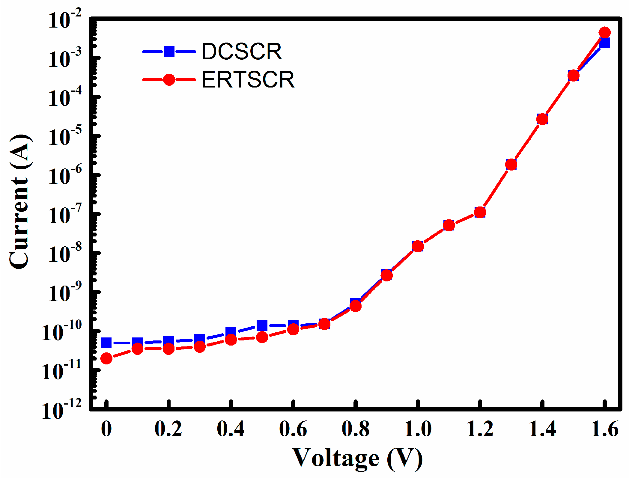
4.3. Leakage Current Characteristics

Leakage current is another critical design metric for the ESD devices [18,19]. Figure 8 shows the measured leakage currents of the conventional DCSCR and proposed ERTSCR, with the anode biased from 0 V to 1.6 V and the cathode grounded. It can be seen that the leakage currents are less than 1 μA when biased below 1.2 V, which shows that both structures are suitable for the ESD protection of the ICs working at 1.2 V or below [20]. As the biased voltage continuously increases, both the leakage currents quickly increase with the turning on of the two diodes and following SCR.

5. Conclusions

An ESD protection device is presented in this article as an embedded resistor-triggered SCR. The proposed ERTSCR has a low trigger voltage, high second breakdown currents and acceptable leakage current. With comparable ESD robustness to conventional DCSCR, the proposed ERTSCR has a wider top metal width and an area cost reduction of approximately 10%.

Author Contributions

Conceptualization, F.H. and Z.L.; methodology, F.H. and F.D; software, K.Y. and J.L.; validation, F.H., F.D. and K.Y.; formal analysis, K.Y.; investigation, F.H. and F.D; resources, J.L.; data curation, F.H.; writing—original draft preparation, F.H.; writing—review and editing, J.L. and Z.L.; visualization, J.L.; supervision, Z.L.

Funding

This research was funded by the Nature Science Foundation of China 61874098, Central Universities Fundamental Research Project ZYGX2018J025 and Sichuan Science and Technology Basic Condition Platform Project 18PTDJ0053.

Conflicts of Interest

The authors declare no conflict of interest.

References

  1. Salcedo, J.A.; Liou, J.J.; Bernier, J.C. Design and integration of novel SCR-based devices for ESD protection in CMOS/BiCMOS technologies. IEEE Trans. Electron Devices 2005, 52, 2682–2689. [Google Scholar] [CrossRef]
  2. Ker, M.D.; Hsu, K.C. Overview of on-chip electrostatic discharge protection design with SCR-based devices in CMOS integrated circuits. IEEE Trans. Device Mater. Reliab. 2005, 5, 235–249. [Google Scholar] [CrossRef]
  3. Duvvury, C.; Rountree, R. A synthesis of ESD input protection scheme. J. Electr. 1992, 29, 88–97. [Google Scholar] [CrossRef]
  4. Ker, M.D.; Wu, C.Y.; Chang, H.H. Complementary-LVTSCR ESD protection circuit for submicron CMOS VLSI/ULSI. IEEE Trans. Electron Devices 1996, 43, 588–598. [Google Scholar] [CrossRef]
  5. Ma, F.; Han, Y.; Dong, S.; Miao, M.; Liang, H. Improved Low-Voltage-Triggered SCR Structure for RF-ESD Protection. IEEE Electron Device Lett. 2013, 34, 1050–1052. [Google Scholar] [CrossRef]
  6. Russ, C.; Mergens, M.; Verhaege, K.; Armer, J.; Jozwiak, P.; Kolluri, G.; Avery, L. GGSCR: GGNMOS triggered silicon controlled rectifiers for ESD protection in deep submicron CMOS processes. In Proceedings of the 2001 IEEE Electrical Overstress/Electrostatic Discharge Symposium (EOS/ESD), Portland, OR, USA, 11–13 September 2001; pp. 22–31. [Google Scholar]
  7. Mergens, M.; Russ, C.C.; Verhaege, K.G.; Armer, J.; Jozwiak, P.C.; Mohn, R.P.; Keppens, B.; Trunh, C.S. Speed optimized Diode-Triggered SCR (DTSCR) for RF ESD protection of Ultra-Sensitive IC nodes in advanced technologies. IEEE Trans. Device Mater. Reliab. 2005, 5, 532–542. [Google Scholar] [CrossRef]
  8. Lin, C.; Fan, M. Optimization on Layout Style of Diode Stackup for On-Chip ESD Protection. IEEE Trans. Device Mater. Reliab. 2014, 14, 775–777. [Google Scholar] [CrossRef]
  9. Sun, R.C.; Wang, Z.; Klebanov, M.; Liang, W.; Liou, J.J.; Liu, D.G. Silicon-Controlled Rectifier for Electrostatic Discharge Protection Solutions with Minimal Snapback and Reduced Overshoot Voltage. IEEE Electron Device Lett. 2015, 36, 424–426. [Google Scholar] [CrossRef]
  10. Chen, J.; Lin, C.; Ker, M. On-Chip ESD Protection Device for High-Speed I/O Applications in CMOS Technology. IEEE Trans. Electron Devices 2017, 64, 3979–3985. [Google Scholar] [CrossRef]
  11. Lin, C.; Chen, C. Resistor-Triggered SCR Device for ESD Protection in High-Speed I/O Interface Circuits. IEEE Electron Device Lett. 2017, 38, 712–715. [Google Scholar] [CrossRef]
  12. Dong, A.; Salcedo, J.A.; Parthasarathy, S.; Zhou, Y.; Luo, S.; Hajjar, J.J.; Liou, J.J. ESD protection structure with reduced capacitance and overshoot voltage for high speed interface applications. Microelectron. Reliab. 2017, 79, 201–205. [Google Scholar] [CrossRef]
  13. Lin, C.; Chen, C. Low-C ESD Protection Design with Dual Resistor-Triggered SCRs in CMOS Technology. IEEE Trans. Device Mater. Reliab. 2018, 18, 197–204. [Google Scholar] [CrossRef]
  14. Du, X.; Dong, S.; Han, Y.; Liou, J.J. Analysis of metal routing technique in a novel dual direction multi-finger SCR ESD protection device. In Proceedings of the 2008 IEEE International Conference on Solid-State and Integrated-Circuit Technology (ICSICT), Beijing, China, 20–23 October 2008; pp. 337–340. [Google Scholar] [CrossRef]
  15. Wang, Z.; Liou, J. Evaluation of geometry layout and metal pattern to optimize ESD performance of silicon controlled rectifier (SCR). In Proceedings of the 2014 IEEE International Reliability Physics Symposium (IRPS), Waikoloa, HI, USA, 1–5 June 2014; pp. EL2.1–EL2.4. [Google Scholar] [CrossRef]
  16. Zhang, Y.; Zhang, H.; Chiu, C.; Tian, H. ESD damage mechanism study of metal fuse area. In Proceedings of the 2016 International Conference on Electronic Packaging Technology (ICEPT), Wuhan, China, 16–19 August 2016; pp. 1427–1429. [Google Scholar] [CrossRef]
  17. Gauthier, R.; Abou-Khalil, M.; Chatty, K.; Mitra, S.; Li, J. Investigation of Voltage Overshoots in Diode Triggered Silicon Controlled Rectifiers (DTSCRs) Under Very Fast Transmission Line Pulsing (VFTLP). In Proceedings of the 2009 IEEE Electrical Overstress/Electrostatic Discharge Symposium (EOS/ESD), Anaheim, CA, USA, 30 August–13 September 2009; pp. 1–10. [Google Scholar]
  18. Ker, M.; Lo, W. Design on the Low-Leakage Diode String for Using in the Power-Rail ESD Clamp Circuits in a 0.35-μm Silicide CMOS Process. IEEE Trans. Solid-State Circuits 2000, 35, 601–611. [Google Scholar] [CrossRef]
  19. Chen, S.; Chen, T.; Tang, T.; Chen, J.; Chou, C. Low-Leakage Diode String Designs Using Triple-Well Technologies for RF-ESD Applications. IEEE Electron Device Lett. 2003, 24, 595–597. [Google Scholar] [CrossRef]
  20. Lin, C.; Wu, P.; Ker, M. Area-Efficient and Low-Leakage Diode String for On-Chip ESD Protection. IEEE Trans. Electron Devices 2016, 63, 531–536. [Google Scholar] [CrossRef]
Figure 1. (a) Cross-sectional view of conventional DCSCR. The trigger path is illustrated by a blue arrow that is called the diode chain path; (b) Equivalent circuit diagram of conventional DCSCR.
Electronics 08 00445 g001
Figure 2. (a) Cross-sectional view of proposed ERTSCR. The DNW acts as an embedded well resistor RDNW in the trigger path; (b) Equivalent circuit diagram of proposed ERTSCR.
Electronics 08 00445 g002
Figure 3. Total current density distributions at different current levels in DCSCR. (a) The trigger current flows along diode chain path; (b) the parasitic NPN and PNP transistors turn on; (c) the SCR path is triggered; and (d) the ESD current distribution after holding point.
Electronics 08 00445 g003
Figure 4. Total current density distributions at different current levels in proposed ERTSCR. (a) The trigger current flows along diode chain path; (b) the parasitic NPN and PNP transistors turn on; (c) the SCR path is triggered; and (d) the ESD current distribution after holding point.
Electronics 08 00445 g004
Figure 5. Layout top views and device dimensions of (a) conventional DCSCR; and (b) proposed ERTSCR. Both DCSCR and ERTSCR have a same device width of 75 μm.
Electronics 08 00445 g005
Figure 6. Measured TLP I-V curves of conventional DCSCR and proposed ERTSCR.
Electronics 08 00445 g006
Figure 7. Measured VF-TLP I-V curves and transient voltage waveforms of conventional DCSCR and proposed ERTSCR.
Electronics 08 00445 g007
Figure 8. Measured leakage currents of conventional DCSCR and proposed ERTSCR.
Electronics 08 00445 g008

