1. Introduction
With the rapid increase in the amount of data transmitted over telecommunications networks, interest in high speed optoelectronic devices and systems has increased. The high demand for large data transmission rates has led to the rapid development of data transmission technology. With the continuous increase of data traffic in modern communication networks, the data rate between system nodes has approached the physical limit of general links such as copper wires. Therefore, an urgent need is to increase the communication speeds of these networks. Owing to its high bandwidth, the optical fiber is the favorite medium chosen to meet this need in today’s information based society [
1,
2,
3,
4]. Our research efforts are aimed in this direction [
5,
6,
7].
The recent dramatic growth of Internet data volume and speed entails the development of low cost integrated optical communication systems with a high transmission bandwidth [
8]. The analog optical receiver that incorporates a TIA input stage and post-amplifying stages plays a critical role in the whole optical communication system [
9]. The TIA is the first electrical building block in the analog optical receiver. Its function is to convert the induced photodiode (PD) current into a large voltage signal to be used in the digital processing unit. The TIA is required to have both high gain and wide bandwidth along with low power dissipation [
10,
11,
12,
13,
14,
15,
16,
17,
18,
19,
20,
21,
22,
23,
24,
25,
26,
27,
28,
29,
30,
31,
32,
33].
Several research articles on improving the bandwidth of TIA have been published. In particular, inductive peaking has been extensively used to improve the bandwidth and decrease parasitic capacitance effects. The inductor is one of the most important elements in TIAs for high frequency applications and RF systems. However, its extremely large size makes the TIA chip large and expensive. Hence, decreasing the area of the inductors used in TIA design is very important. In the gyrator realization, the active inductor (AI) is constructed by connecting two differential transconductors back-to-back in negative feedback. The parasitic capacitance of the basis transistors is the load capacitance in the gyrator-C topology.
Furthermore, a bandwidth enhancement method based on the interaction of a matching LC network, a regulated cascode (RGC) input stage, and a capacitive degeneration stage can be used to enhance the bandwidth and provide efficient noise reduction. This turns the TIA into a fifth-order Butterworth low pass filter. In this paper, we propose a novel wideband TIA using the Mahmoudi–Salama floating-type AI, which is based on the gyrator-C topology.
This proposed TIA based on floating AI not only has the advantages of a wide bandwidth of 10 GHz and a transimpedance gain of 41 dB
, it also has the merits of a smaller chip area and lower power dissipation compared with the conventional TIA, based on a spiral inductor [
8]. However, owing to the use of floating active inductors, this proposed TIA has the inherent disadvantage of reduced input referred noise performance in comparison to the conventional TIA, made of a spiral inductor [
8]. In this paper, the design and post-layout simulation results of a 10 GHz 0.18
m CMOS TIA are presented.
The remainder of this paper is organized as follows.
Section 2 describes the conventional TIA based on the traditional broadband design technique.
Section 3 discusses the basic principle of gyrator-C networks and introduces the gyrator based differential FAIused to replace the spiral inductor in the conventional TIA. The proposed TIA based on the FAI is presented in
Section 4. The simulation results are presented in
Section 5, and finally, the conclusions are summarized in
Section 6.
2. TIA Based on the Traditional Broadband Design Technique
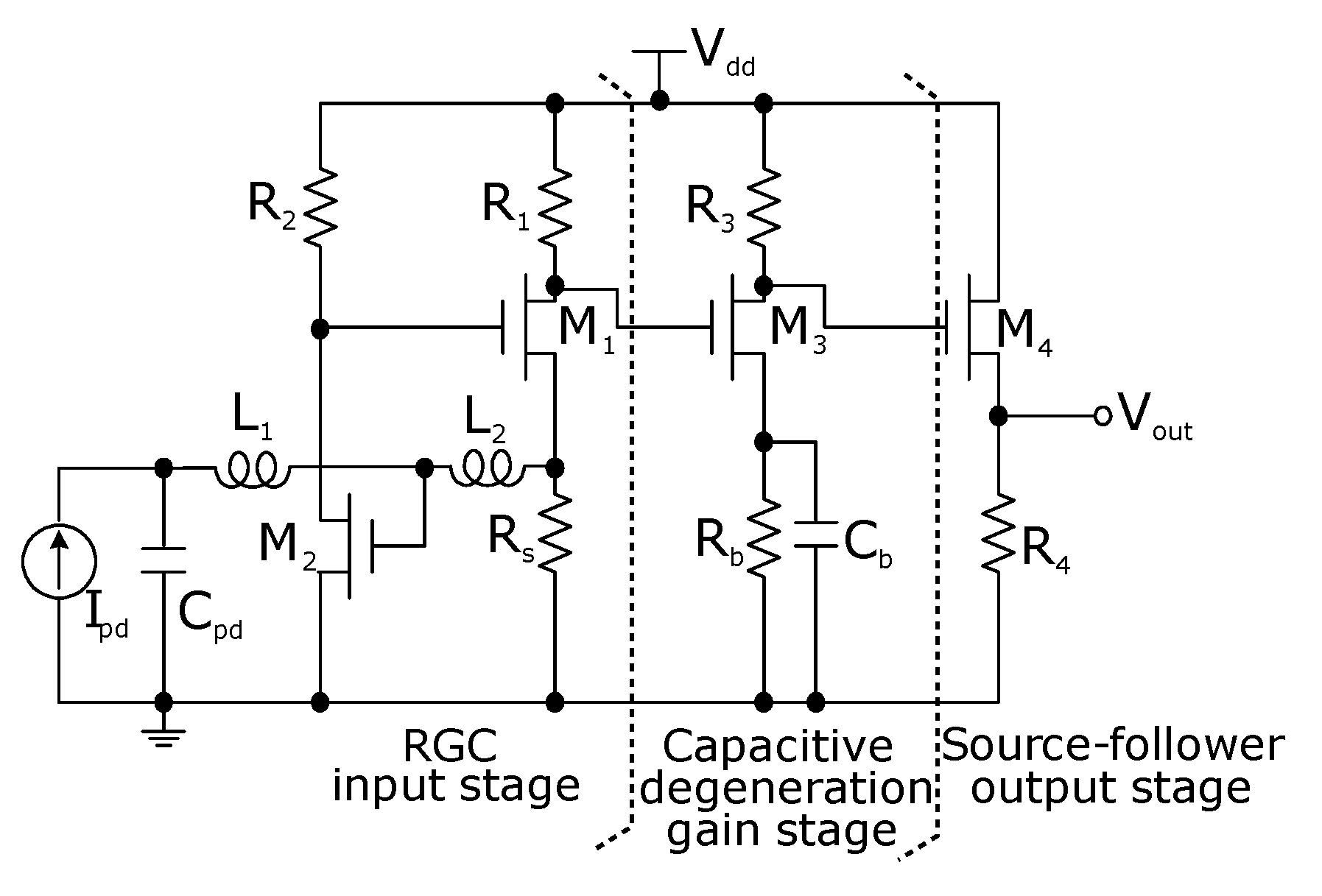
Figure 1 represents the schematic of a TIA based on the traditional broadband design technology. The TIA was composed of the following four parts: a matching network, an RGCinput stage, a gain stage with capacitive degeneration, and a source follower output stage [
8]. Because the input impedance of the RGC stage was very small, the lowest pole of the circuit was located within the TIA. In this TIA, a small
was chosen to avoid possible peaking due to the zero generated by the local feedback of the RGC stage. Moreover, relatively large
were selected to minimize the noise current and signal loss. The capacitive degeneration gain stage consisted of
,
, and
, and
contributed a zero
that was used to compensate the lowest pole determined.
and
formed the source follower output stage used to drive the capacitance of the output pad.
3. Lossless Floating Gyrator-C Active Inductors
3.1. Principles of Gyrator-C Active Inductors
The inductor is one of the most important circuit elements in high frequency applications and RF systems. CMOS AIs have become a very hot research topic in recent years due to their many advantages over passive inductors. AI systems can be implemented by circuits that occupy a small chip area. In addition, AIs have large variable inductance and a high quality factor. In contrast, compared with spiral inductors, AIs have some disadvantages such as poor noise performance, small dynamic range, and sensitivity to the process. Bandwidth extension topologies typically use on-chip inductors to compensate for capacitive effects, but the associated hardware costs are high. Therefore, it is very important to reduce the area of the inductor used in TIA design.
An AI was constructed with a small number of transistors. The gyrator was implemented using two transconductances connected back-to-back [
18]. When the port of the gyrator is connected to a capacitor, as shown in
Figure 2, the network is called the gyrator-C network. A gyrator-C network is said to be lossless when both the input and output impedances of the system’s transconductor of the system are infinite, and the transconductances of the transconductors are constant.
The admittance looking into port 2 of the gyrator-C network is given by:
Equation (
1) indicates that the port 2 of the gyrator-C network behaves as a floating inductor with inductance given by:
3.2. Mahmoudi and Salama Active Inductor
The floating active inductor proposed by Mahmoudi and Salama is used in the design of quadrature down converters for wireless applications [
15,
21]. The schematic of the the floating active inductor is shown in
Figure 3. It mainly consisted of a pair of differential transconductors and a pair of negative resistors at the output of the transconductors.
and
were biased in the triode and behaved as voltage controlled resistors. They were added to the conventional cross-coupled configuration of negative resistors to provide resistance tunability for the negative resistors, without using a tail current source. The common-mode stabilizer consisted of a cross-coupled differential pair
,
(
,
) and transistor
(
), which was designed to operate in triode mode. The stabilizer was added to the design to stabilize the common-mode behavior of the differential active inductor by moving the common-mode right half-plane pole of the inductor, which may cause instability, to the left-half-plane. In the differential mode of operation, the common-mode stabilizer appeared as an impedance
with a real part given by [
34]:
where
is the transconductance of
or
and
is the output resistance of
in the triode region, which can be controlled by the voltage
. Hence, the stability of the active inductor was improved.
Figure 4 shows clearly that the Mahmoudi–Salama AI was based on the gyrator-C structure. According to the inductance relationship of (
2), when the gyrator-C network appeared as a FAI described in
Section 3.1, we could obtain:
where
and
are the transconductances of
(
) and
(
), respectively.
The frequency response of the Mahmoudi and Salama AI as obtained through simulation is shown in
Figure 5. We can see that the FAI had a good inductance characteristic when the frequency was within 100 GHz.
4. Proposed TIA
4.1. Circuit Topology
The RGC input stage was well suited for broadband TIA design by its very low input impedance, compared with a single common-source follower and an inverter based amplifier. Thus, in this paper, the proposed TIA was based on an RGC TIA, as shown in
Figure 1. To reduce the chip area of TIA, an inductor
was composed by an active inductor, which was named the Mahmoudi and Salama active inductor. Due to its good stability, we chose this type of active inductor (see
Section 3.2).
4.2. Circuit Structure
The conventional TIA is shown in
Figure 1, where
and
are spiral inductors. In this work, we changed spiral inductor
with the Mahmoudi–Salama FAI. Unlike the conventional TIA in [
1], in this work, we assumed that
was constructed by bonding wires. It is well known that in general processes, the inductance of a 1 mm bonding wire is between 2 nH and 2.5 nH. Therefore, we assumed that the bonding wire, not on-chip, was the inductor
, as shown in
Figure 1. In
Section 5, we provide post-layout simulation results that indicated that the value of
was between 2 nH and 3 nH.
As mentioned in
Section 2, the proposed TIA was composed of four parts: a matching network, an RGC input stage, a gain stage with capacitive degeneration, and a source follower output stage.
4.3. Small Signal Analysis of the RGC Stage in TIA
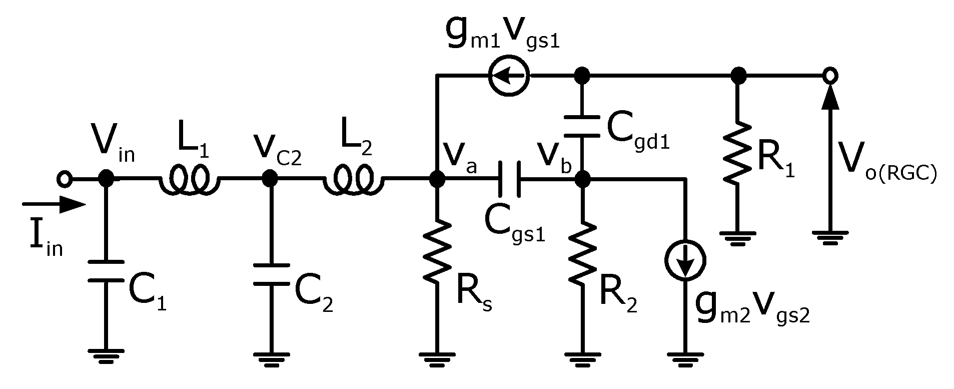
Figure 6 illustrates the small signal model of the matching network and the RGC input stage. As described in
Section 2, in the RGC stage of the proposed TIA, we chose a small
to avoid possible peaking due to the zero generated by the local feedback of the RGC stage. Here, through small signal analysis, we discuss the effects of the inductors
,
, and
on the proposed TIA.
Here, the input impedance
can be obtained as:
From Equations (5) and (6), the expression of the transimpedance gain is obtained as shown in (7). In addition, we have the DC gain of the RGC as shown in Equation (8).
The original RGC gain was
, as shown in (8). In order to make the gain as large as possible, the term of
must be increased, that is the value of
needs to be increased or the value of
needs to be decreased. However, in this TIA,
was the inductance of the bonding wire, which was almost fixed. As can be seen from
Figure 5, the inductance of this FAI was very small. Therefore, we increased
above 500
to increase the gain appropriately. Furthermore, a relatively large
could minimize noise current contribution and the signal loss due to it.
4.4. Noise Analysis
The TIA model with series inductive matching between the photodiode and the amplifier is renowned to be very helpful in reducing the frequency dependent noise and improving the front-end sensitivity [
8,
35]. In [
8], the equivalent input noise current spectral density of RGC TIA with inductor peaking was approximated as:
where
stands for the photodiode parasitic capacitance. For a given
noise model (see [
8]),
and
are independent of the input matching network. Since
is a negative term in (9), the noise reduction effect of
can be clearly indicated. The effect of
is similar to that of
. However, the effective inductance of
is
, which is relatively small; hence, the noise reduction effect of
should be less than that of
[
8]. Consequently, we can come to the conclusion that increasing the effective value of the inductor in this topology could reduce the input referred noise, in theory.
5. Post-Layout Simulation Results
To evaluate its performance, the TIA was implemented using 0.18 m Rohm CMOS technology. All post-layout simulation results were performed in Cadence.
The layout of the top cell with the pad and TIA core is shown in
Figure 7 and
Figure 8, respectively. Correspondingly, they occupied layout areas of 1590
m × 780
m and 180
m × 118
m.
Figure 9 shows the chip microphotograph of the proposed TIA.
Figure 10 shows the post-layout frequency response of the proposed TIA. We can see from the simulation results that no matter what value
took between 2 nH and 3 nH, the transimpedance gain was about 41 dB
and the −3 dB bandwidth was greater than 10 GHz in the presence of a
of 150 fF. The conclusion was that any value between 2 nH and 3 nH of the bonding wire worked well with this design and gave good frequency characteristics.
Figure 11 shows the eye-diagram for the input signal currents of 100
pseudo-random bit sequence (PRBS) at the rates of 5 Gb/s, 10 Gb/s, and 15 Gb/s. In this post-layout simulation, the PRBS generator was implemented using linear feed back shift registers (LFSR). These PRBS outputs had a jitter of 2 ps. From the post-layout simulation results, the proposed TIA could generate the waveform with good eye-opening owing to the wide bandwidth. The jitter of the post-layout simulation was 4.03 ps when the bit rate was 15 Gb/s.
Table 1 compares the performance of the proposed TIA with other recently published TIAs. It can be clearly seen that the presented work was superior in terms of bandwidth, power dissipation, and chip area compared with other TIAs implemented using the same 0.18
m CMOS technology.
The standard figure of merit (FoM) is calculated as (10) below and is used to compare this design with other recent TIA designs in
Table 1.
It can be seen that this design was better in terms of FoM compared with the conventional design using the same process. The input referred noise of the proposed TIA was increased by a factor of approximately 1.7, compared with the conventional TIA. The main cause of the increase of input referred noise was that the effective value of the active inductor we used was much smaller than the effective value of the spiral inductor in the conventional TIA. Furthermore, we assumed that the bonding wire was 2 nH to connect the photo-diode (PD). However, in the conventional TIA, the spiral inductor of was 0.77 nH, which was not including the inductance of PD connection. The actual value of in the conventional TIA could be approximately expressed as . In other words, assuming that the inductance of the bonding wire was the same, the effective value of of the conventional TIA was actually 0.77 nH larger than that of the proposed TIA. This also increased the input referred noise to a considerable extent. Nevertheless, the noise performance of the proposed TIA was also better than that of the general TIA without a matching network of inductors.
6. Conclusions
In this paper, we presented a broadband TIA with a floating active inductor exhibiting the following characteristics: a −3 dB bandwidth greater than 10 GHz and a transimpedance gain of 41 dB. Owing to the use of FAI, the area of the chip was greatly reduced and was almost 18.8% of that of the conventional TIA. Moreover, because the parameters and resistance value of the transistor were different from the conventional TIA, the simulation results showed that the floating active inductor did not increase the power dissipation. In contrast, the proposed TIA had a lower power dissipation of 10.7 mW. Thus, the post-layout simulation results indicated that the floating active inductor was very useful in optical applications.
Author Contributions
X.C. and Y.T. contributed to the design of the proposed circuit; X.C. performed the simulations, the layout design, and the writing, original draft; all authors participated in the data analysis and paper revision.
Funding
This research was funded by China Scholarship Council (CSC) (No. 201808050092).
Acknowledgments
This work was supported by the VLSIDesign and Education Center (VDEC), the University of Tokyo, in collaboration with Cadence Corporation and Synopsys, Inc. The VLSI chip in this study was fabricated in the chip fabrication program of VDEC, the University of Tokyo, in collaboration with Rohm Corporation and Toppan Printing Corporation. We would also like to acknowledge the financial support by the China Scholarship Council (CSC) through the award of a Ph.D. scholarship (No. 201808050092) to Xiangyu Chen, which is under the State Scholarship Fund.
Conflicts of Interest
The authors declare no conflict of interest.
References
- Chen, Y.; Wang, Z.; Fan, X.; Wang, H.; Li, W. A 38 Gb/s to 43 Gb/s Monolithic Optical Receiver in 65 nm CMOS Technology. IEEE Trans. Circuit Syst.-I Regular Pap. 2013, 60, 3173–3181. [Google Scholar] [CrossRef]
- Li, D.; Minoia, G.; Repossi, M.; Baldi, D.; Temporiti, E.; Mazzanti, A. A low-noise design technique for high-speed CMOS optical receivers. IEEE J. Solid-State Circuits 2014, 49, 1437–1447. [Google Scholar] [CrossRef]
- Gao, Q.; Xie, S.; Mao, L.; Wu, S.; Gu, Y.; Li, H.; Song, Q. A single-to-differential broadband transimpedance amplifier for 12.5 Gb/s optical links. IEICE Electron. Express 2016, 14, 1–12. [Google Scholar] [CrossRef] [Green Version]
- Andrews, C.; Diamente, L.; Yang, D.; Johnson, B.; Molnar, A. A low-noise design technique for high-speed CMOS optical receivers. IEEE J. Solid-State Circuits 2013, 48, 1188–1198. [Google Scholar] [CrossRef]
- Park, S.M.; Yoo, H.-J. 1.25-Gb/s regulated cascode CMOS transimpedance amplifier for Gigabit Ethernet applications. IEEE J. Solid-State Circuits 2004, 39, 112–121. [Google Scholar] [CrossRef] [Green Version]
- Huangs, S.-H.; Chen, W.-Z.; Chang, Y.-W.; Huang, Y.-T. A 10-Gb/s OEIC with meshed spatially-modulated photo detector in 0.18-μm CMOS technology. IEEE J. Solid-State Circuits 2011, 46, 1158–1169. [Google Scholar] [CrossRef]
- Park, K.-Y.; Oh, W.-S.; Choi, W.Y. A 10-Gb/s trans-impedance amplifier with LC-ladder input configuration. IEICE Electron. Express 2010, 7, 1201–1206. [Google Scholar] [CrossRef] [Green Version]
- Lu, Z.; Yeo, K.S.; Ma, J.G. Broad-band design techniques for transimpedance amplifiers. IEEE Trans. Circuit Syst.-I Regular Pap. 2007, 54, 590–600. [Google Scholar] [CrossRef]
- Zhang, Z.; Chen, Y.; Li, J.; Wang, H.; Guo, C.; Zhang, J. A low-noise 71-dBΩ transimpedance 31-GHz bandwidth optical receiver with automatic gain control in 0.13-μm SiGe BiCMOS. IEICE Electron. Express 2019, 16, 1–8. [Google Scholar] [CrossRef]
- Analui, B.; Hajimiri, A. Bandwidth enhancement for transimpedance amplifiers. IEEE J. Solid-State Circuits 2004, 39, 1263–1270. [Google Scholar] [CrossRef]
- Oh, Y.-H.; Lee, S.-G. An inductance enhancement technique and its application to a shunt-peaked 2.5 Gb/s transimpedance amplifier design. IEEE Trans. Circuit Syst.-II Express Briefs 2004, 51, 624–628. [Google Scholar] [CrossRef]
- Kromer, C.; Sialm, G.; Morf, T.; Schmatz, M.L.; Ellinger, F.; Erni, D.; Jackel, H. A Low-Power 20-GHz 52-dBΩ transimpedance amplifier in 80-nm CMOS. IEEE J. Solid-State Circuits 2004, 39, 858–894. [Google Scholar] [CrossRef]
- Wu, C.-H.; Lee, C.-H.; Chen, W.-S.; Liu, S.-L. CMOS wideband amplifiers using multiple inductive-series peaking technique. IEEE J. Solid-State Circuits 2005, 40, 548–552. [Google Scholar] [CrossRef]
- Chen, W.-Z.; Lu, C.-H. Design and analysis of a 2.5-Gbps optical receiver analog front-end in a 0.35-μm digital CMOS technology. IEEE Trans. Circuit Syst.-I Regular Pap. 2006, 53, 977–983. [Google Scholar] [CrossRef]
- Mahmoudi, F.; Salama, C.A. 8 GHz 1V, CMOS quadrature downconverter for wireless applications. Analog. Integr. Circuits Signal Process. 2006, 48, 185–197. [Google Scholar] [CrossRef]
- Choi, B.-Y.; Han, J.-W.; Park, S.M.; Park, K.; Oh, W.-S.; Choi, J.-C. A 1Gb/s optical transceiver array chipset for automotive wired interconnects. In Proceedings of the IEEE International Symposium on Circuits and Systems, New Orleans, LA, USA, 27–30 May 2007. [Google Scholar] [CrossRef]
- Jin, J.-D.; Hsu, S.S.H. A 40-Gb/s transimpedance amplifier in 0.18-μm CMOS technology. IEEE J. Solid-State Circuits 2008, 43, 1449–1457. [Google Scholar] [CrossRef]
- Fei, Y. CMOS Active Inductors and Transformers; Springer: Boston, MA, USA, 2008. [Google Scholar]
- Chen, H.-L.; Chen, C.-H.; Yang, W.-B.; Chiang, J.-S. Inductorless CMOS Receiver Front-End Circuits for 10-Gb/s Optical Communications. Tamkang J. Sci. Eng. 2009, 12, 449–458. [Google Scholar] [CrossRef]
- Lu, Z.; Yeo, K.S.; Lim, W.M.; Do, M.A.; Boon, C.C. Design of a CMOS broadband transimpedance amplifier with active feedback. IEEE Trans. Very Large Scale Integr. 2010, 18, 461–472. [Google Scholar] [CrossRef]
- Mahmoudi, F. Quadrature Down-Converter for Wireless Communications. Ph.D. Thesis, University of Toronto, Toronto, ON, Canada, 2012. [Google Scholar]
- Atef, M.; Zimmermann, H. 10Gbit/s 2mW inductorless transimpedance amplifier. In Proceedings of the IEEE International Symposium on Circuits and Systems, Seoul, Korea, 20–23 May 2012. [Google Scholar]
- Kimura, H.; Aziz, P.M.; Jing, T.; Sinha, A.; Kotagiri, S.P.; Narayan, R.; Gao, H.; Jing, P.; Hom, G.; Liang, A.; et al. A 28 Gb/s 560 mW multi-Standard SerDes with single-stage analog front-end and 14-Tap decision feedback equalizer in 28 nm CMOS. IEEE J. Solid-State Circuits 2014, 49, 3091–3103. [Google Scholar] [CrossRef]
- Mizuno, S.; Naito, F.; Nakamura, M. Bandwidth enhancement technique for TIA using flipped voltage follower. IEICE Electron. Express 2017, 14, 1–6. [Google Scholar] [CrossRef] [Green Version]
- Samuel, L.B.S.; Sern, T.Y.; Kumar, T.B.; Seng, Y.K.; Li, Z.; Yu, X. An inductorless transimpedance amplifier design for 10 Gb/s optical communication using 0.18-μm CMOS. In Proceedings of the IEEE International Symposium on Integrated Circuits, Singapore, 12–14 December 2016. [Google Scholar]
- Jawdat, A.-T.; Metin, Y. A 7 GHz compact transimpedance amplifier TIA in CMOS 0.18 μm technology. Analog. Integr. Circuits Signal Process. 2016, 86, 429–438. [Google Scholar] [CrossRef]
- Chen, X.; Takahashi, Y. Evaluation of wide-band frequency trans-impedance amplifier using active inductors. In Proceedings of the IEICE ICD-CPSY-CAS, Ishigaki Island, Japan, 14–15 December 2017. [Google Scholar]
- Chen, X.; Takahashi, Y. Design and analysis of a 10 GHz trans-impedance amplifier using active inductor in 0. In 18 μm CMOS process technology. In Proceedings of the 2018 International Conference on Analog VLSI Circuits, Chiang Mai, Thailand, 31 October–2 November 2018. [Google Scholar]
- Chen, C.; Cai, Z. A 2.4 GHz 2.2 mW current reusing passive mixer with gm-boosted common-gate TIA in 180 nm CMOS. IEICE Electron. Express 2019, 16, 1–7. [Google Scholar] [CrossRef]
- Razavi, B. A 622 Mb/s 4.5 pA/ CMOS transimpedance amplifier [for optical receiver front-end]. In Proceedings of the 2000 IEEE International Solid-State Circuits Conference, San Francisco, CA, USA, 9 February 2000. [Google Scholar]
- Seifouri, M.; Amiri, P.; Rakide, M. Design of broadband trans-impedance for optical communication systems. Microelectron. J. 2015, 46, 679–684. [Google Scholar] [CrossRef]
- Wang, C.-Y.; Wang, C.-S.; Wang, C.-K. An 18mW two Stage CMOS transimpedance amplifier for 10 Gb/s Optical application. In Proceedings of the 2007 IEEE Asian Solid-State Circuits Conference, Jeju, Korea, 12–14 November 2007. [Google Scholar]
- Schrodinger, K.; Stimma, J.; Mauthe, M. A fully integrated CMOS receiver front-end for optic Gigabit Ethernet. IEEE J. Solid-State Circuits 2002, 37, 574–880. [Google Scholar] [CrossRef]
- Mahmoudi, F.; Salama, C.A. 8 GHz Tunable CMOS Quadrature Generator using Differential Active Inductors. In Proceedings of the IEEE International Symposium on Circuits and Systems, Kobe, Japan, 23–26 May 2005. [Google Scholar]
- Park, M.S.; Minasian, R.A. Ultra-low-noise and wideband-tuned optical receiver synthesis and design. J. Lightwave Technol. 1994, 12, 254–259. [Google Scholar] [CrossRef]
- Szilagyi, L.; Henker, R.; Ellinger, F. An Inductor-less Ultra-Compact Transimpedance Amplifier for 30 Gbps in 28 nm CMOS with High Energy-Efficiency. In Proceedings of the 2014 IEEE 57th International Midwest Symposium on Circuits and Systems (MWSCAS), College Station, TX, USA, 3–6 August 2014. [Google Scholar]
© 2019 by the authors. Licensee MDPI, Basel, Switzerland. This article is an open access article distributed under the terms and conditions of the Creative Commons Attribution (CC BY) license (http://creativecommons.org/licenses/by/4.0/).


