Article

SEE Sensitivity Evaluation for Commercial 16 nm SRAM-FPGA

1
Institute of Modern Physics, Chinese Academy of Sciences, Lanzhou 730000, Gansu, China
2
School of Nuclear Science and Technology, University of Chinese Academy of Sciences, Beijing 100049, China
3
State Key Laboratory of ASIC and System, Fudan University, Shanghai 201203, China
4
Department of Computer Science and Technology, Tsinghua University, Beijing 100084, China
5
National Supercomputing Center in Wuxi, Wuxi 214000, Jiangsu, China
*
Authors to whom correspondence should be addressed.
Electronics 2019, 8(12), 1531; https://doi.org/10.3390/electronics8121531
Submission received: 30 October 2019 / Revised: 3 December 2019 / Accepted: 9 December 2019 / Published: 12 December 2019
(This article belongs to the Special Issue Extreme-Environment Electronics: Challenges and Solutions)

Abstract

:
Radiation effects can induce severe and diverse soft errors in digital circuits and systems. A Xilinx commercial 16 nm FinFET static random-access memory (SRAM)-based field-programmable gate array (FPGA) was selected to evaluate the radiation sensitivity and promote the space application of FinFET ultra large-scale integrated circuits (ULSI). Picosecond pulsed laser and high energy heavy ions were employed for irradiation. Before the tests, SRAM-based configure RAMs (CRAMs) were initialized and configured. The 100% embedded block RAMs (BRAMs) were utilized based on the Vivado implementation of the compiled hardware description language. No hard error was observed in both the laser and heavy-ion test. The thresholds for laser-induced single event upset (SEU) were ~3.5 nJ, and the SEU cross-sections were correlated positively to the laser’s energy. Multi-bit upsets were measured in heavy-ion and high-energy laser irradiation. Moreover, latch-up and functional interrupt phenomena were common, especially in the heavy-ion tests. The single event effect results for the 16 nm FinFET process were significant, and some radiation tolerance strategies were required in a radiation environment.

1. Introduction

Given its high processing power and configuration flexibility, static random-access memory (SRAM)-based field-programmable gate array (FPGA) has become one of the most fascinating devices in astrionics [1,2,3]. However, particle-induced single event effects (SEE) in SRAM-FPGA have shown diversity and complexity in previous studies. This was because the basic SRAM architectures were sensitive to single event upset (SEU), single event latch-up (SEL), and single event functional interrupt (SEFI). The corruption of logic values like SEU, disturbance of the functionalities like SEFI, and the thermal damage of circuits like SEL have different effects on the FPGA [1,2,3]. Though SEU is not so destructive as SEL, the occurrence of upset errors in FPGA configure RAMs (CRAMs) may change the internal states of the circuits. This may propagate to the primary outputs of circuits and produce bit errors, or even cause system failures [3,4,5,6,7]. Thus, some typical radiation-hardened FPGAs have been designed and widely employed in space missions [3,6,7,8]. However, the rapid advances of commercial-off-the-shelf (COTS) in the field of integrated circuits (IC) have enabled the use of inexpensive and high-performance electronic components that also contributes to the space industry [9]. As reported in Reference [9,10], in CubeSats or many commercial missions, using COTS components is becoming the rule rather than an exception, and many COTS are complicated systems. However, to reduce risks in the radiation environment, identifying the sensitive and the essential modules for a hardening designer is necessary.
The Xilinx Ultrascale+ FPGA has excellent performance and large storage capacity and it is hugely appealing in data handling. However, the SEU influence and FPGA response are more complicated due to their small feature size, high performance, and special charge collection mechanisms in a radiation environment [3]. Apart from the fault injection in the designing procedure, the irradiation results are more direct and effective to characterize the sensitivity of FPGA. Though several details about alpha particles, neutrons, and protons were reported, the heavy-ion and laser irradiation results are very limited for the CRAM and BRAM module in Ultrascale+ FPGA. Moreover, systematic SEE results are essential for the module’s potential applications in the radiation environment [11]. Further, FPGA irradiation data will have a guiding significance for logic protections in the design flow and utilization of error mitigation strategies at a system level [1,3].
The paper is organized as follows: The device under test (DUT) and testing methods are provided in Section 2. We describe the irradiation parameters and experimental details in Section 3. The heavy-ion and pulse laser irradiation results are presented in Section 4 and further discussion about the application and error mitigation strategies are shown in Section 5. Finally, we give conclusions.

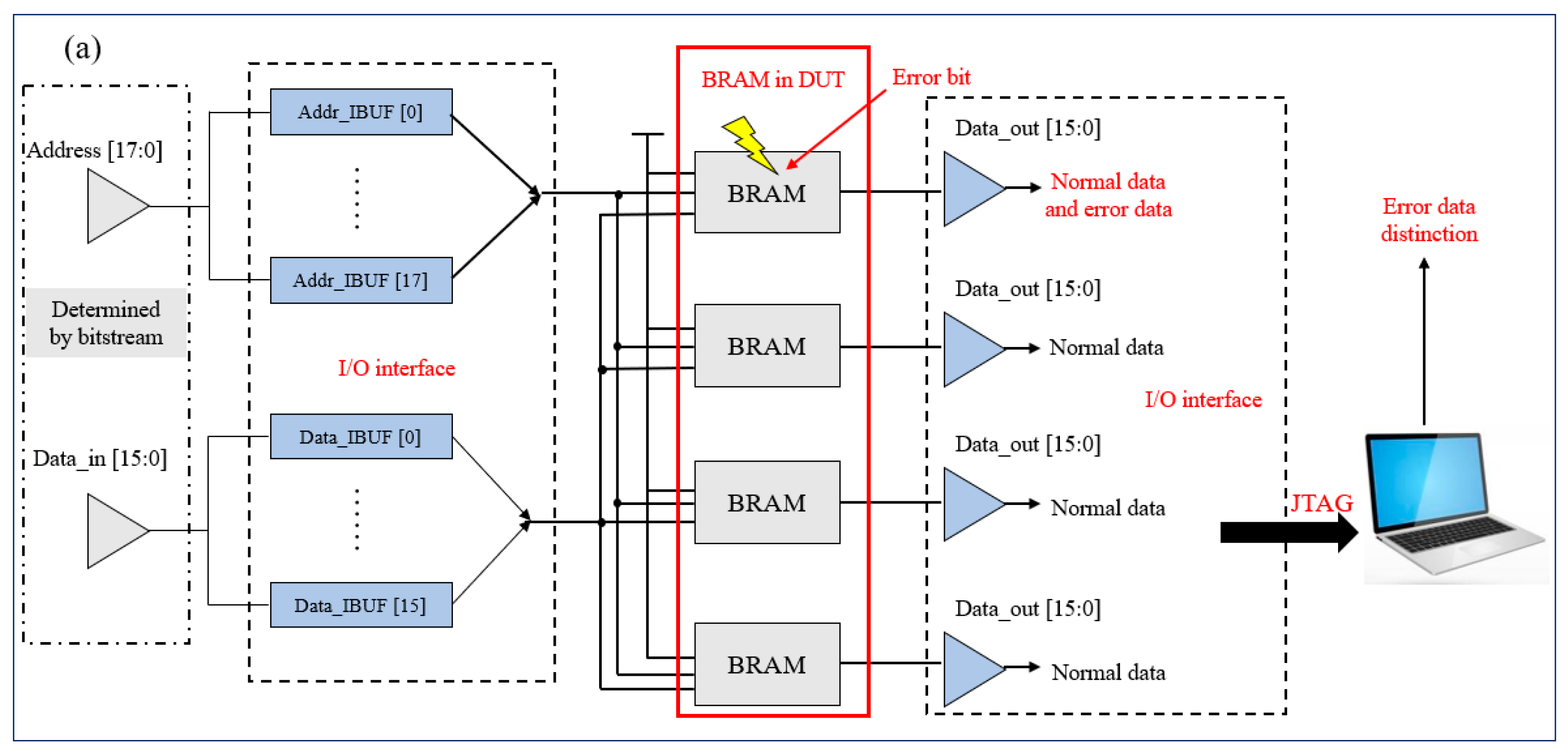
2. DUT Information and Testing Method

The Xilinx KCU116 evaluation platform with Kintex UltraScale+ FPGA (xcku5p-ffvb676-2-e) was used as the DUT to characterize the SEE sensitivities in FinFET ultra large-scale integrated circuits (ULSI). The Verilog hardware description languages were employed to achieve the memory test and functional test. During each trial, all the CRAM in the xcku5p FPGA were measured, and the I/O currents, SEU, and SEFI signals were detected timely.
In case the SEL induced failures, the input/output (I/O) currents were detected by a real-time monitoring software (MaximDigitalPower) matched to the Xilinx Ultrascale+ evaluation board (as shown in Figure 1). Since the SEL may induce destructive thermal damages in DUT, more than triple of the initial current values were regarded as the SEL phenomenon. The SEL can be detected using the software, and then the power will be cut-off automatically in case the current surges. Owing to the power-off procedure, the SEL could also result in the removal of the configured bitstream in the DUT, rendering the SEU and SEFI tests invalid.
The memory test is mainly aimed to examine the SEU response of the CRAM and BRAM cells in the FPGA. The resource utilization for the memory test is shown in Table 1. The basic structure and the data depth for each BRAM module are shown in Figure 2a. We utilized 100% BRAM by four 16-bit width RAM modules. Few flip-flop (FF) and look-up tables (LUT) were occupied in the implemented project, as shown in Table 1. The bitstreams (bit) together with readback (rbd), mask (msd), and logical location (ll) files were generated by the Vivado software and then uploaded to the computer by the Joint Test Action Group (JTAG) interface. The original bitstream was chosen as a golden file. Meanwhile, the readback bitstreams, operated based on the Tool Command Language (TCL) in Vivado, could be generated dynamically and uploaded to a computer to distinguish the upset data. In addition, the C++ based visual interface was designed to achieve the comparative procedure between the golden file and the readback bitstreams. Then the error information was distinguished, classified, and calculated based on the type of resources.
For the functional test, the embedded Microblaze soft (Intellectual Property) IP core was implemented in the DUT. This was done to control the external double data rate (DDR4) synchronous dynamic RAM (SDRAM) using an integrated memory interface generators (MIG) IP. The schematic for the block design is shown in Figure 2b, and the analytical methods for this test are the same as that in the memory test. The peripheral DDR4 SDRAM in the KCU116 evaluation platform was employed to realize an effective evaluation by checking the read and write function of the implemented IPs in the FPGA. This test was a representative example to evaluate the SEFI rate and its influence on the FinFET FPGA. As shown in Table 1, though the BRAM, LUT, I/O resources utilized are below 40%, a lot of logic and clock resources are included in the functional test. The currents and power consumption for the functional test were not very low due to the embedded Microblaze IP. Higher resource occupation may lead to over-temperature, low efficiency of the JTAG interface, and resulting difficulty in fault analysis, which is not easy for the SEE evaluation.

3. Irradiation Setup

3.1. Pulsed Laser Testing System

As shown in Figure 3a, a pulsed laser irradiation platform was employed to evaluate the SEE sensitivity for the DUT. The detailed parameters of the laser for the irradiation test are shown in Table 2. The DUT was placed in a three-dimensional mobile platform that could give the DUT positional parameters directly to realize accurate and stable movement during the test. The high-energy pulsed laser with a 1064 nm center wavelength and 25 ps pulse width was chosen as the radiation source. The backside irradiation with 5 µm spot size was selected, leading the incident photons passing to the active regions directly without considering the high-density metal layers. The lens should move a ▽d towards the DUT to direct the laser focused onto the active areas of the DUT. The value of ∆d can be calculated from the formula
Δ d = T s u b η ( S i )
where η(Si) is the refractive index of silicon, and Tsub is the thickness of the silicon substrate. Moreover, the optical polarization and attenuation module are also required. An energy controlling system with an operational software was applied to control the initial energy (Einitial) changing from ~85 pJ to ~11.6 nJ, while the effective energy in the substrate regions (Eeff−sub) of DUT is given by
E e f f s u b = ( 1 ϵ 2 ϵ 1 ϵ 2 + ϵ 1 ) · E i n i t i a l
where ϵ 1 and ϵ 2 represent the refractive index for air and silicon, respectively. For the memory test, a wide range of laser energies were used, while only inferior laser energies were applicable to the functional test.

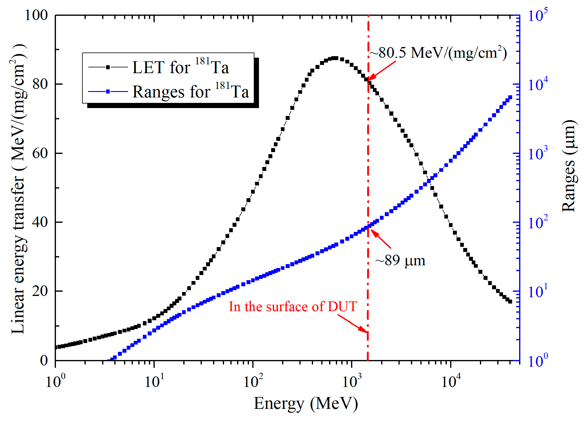
3.2. Heavy Ion Irradiation

The heavy-ion tests were carried out at the Heavy Ion Research Facility in Lanzhou (HIRFL) at the Institute of Modern Physics, Chinese Academy of Sciences. As shown in Figure 3b, at the HIRFL, the test board was located in the air at the end of the terminal, and a laser beamline could be applied to calibrate the position of the DUT. The area of the beamline was 2.30 cm × 2.3 cm, which could realize a fully covered irradiation. The parameters of the LET values and ranges for 181Ta ions are shown in Figure 4. During the irradiation, high energy 181Ta ions were used with the initial linear energy transfer (LET) value at 80.5 MeV·cm2·mg−1. Considering that the DUT is a flip-chip device with ~490 µm silicon on the top of the die, the silicon substrate was thinned down to 60 µm. This was less than the range of incident ions (~99.3 µm in air/~89.0 µm in DUT surface). Furthermore, the flux of incident ions was controlled in ~3 to ~10 ions·cm−2·s−1 in case the current surged.

4. Experimental Results

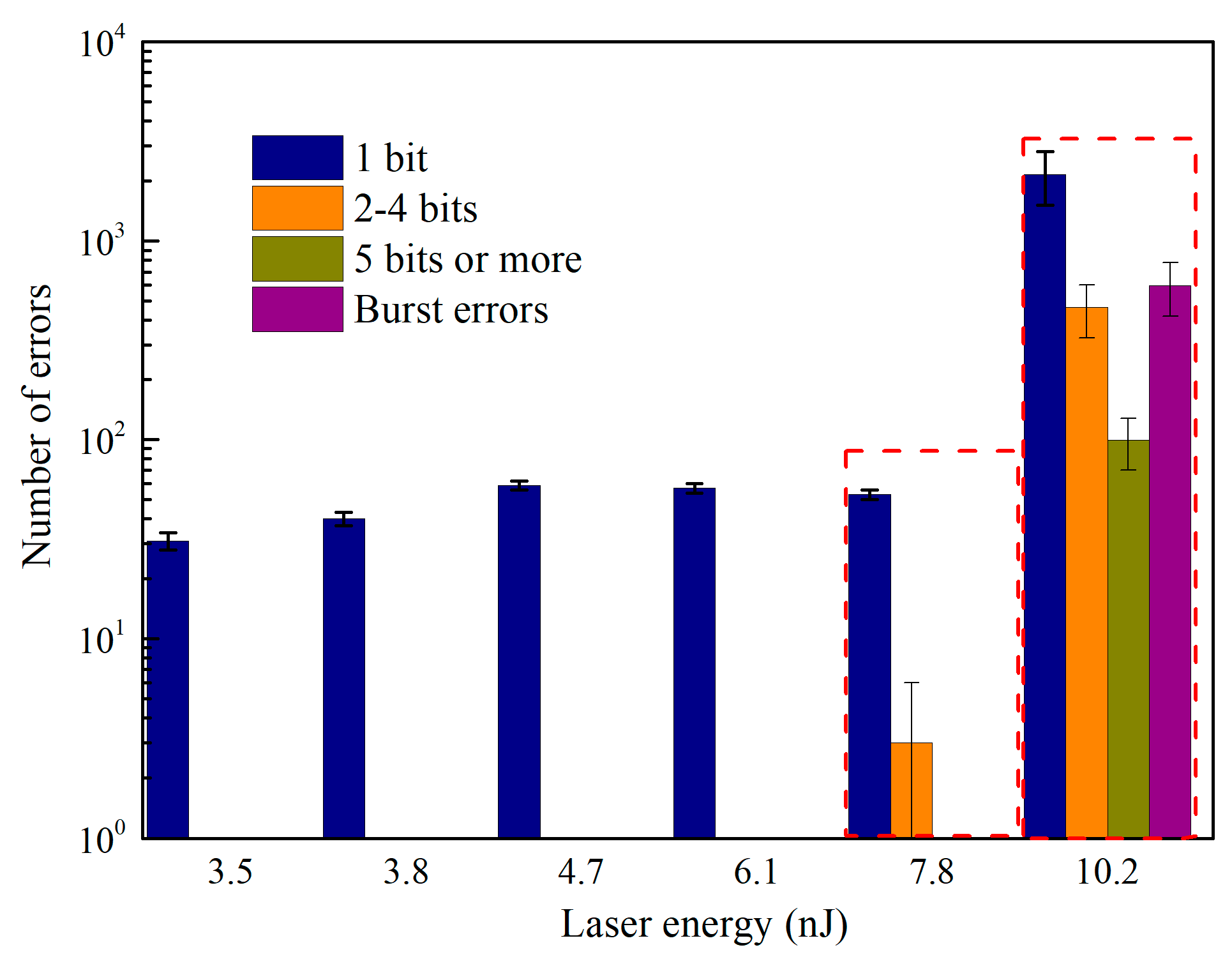
4.1. Pulsed Laser Results

The voltage variations in multiple channels are shown in Figure 5a, and the detailed changes of voltages and currents in a single port are shown in Figure 5b. The voltages and I/O currents were basically stable when the energy of the pulsed laser was below 11.6 nJ.
In the memory test, the full-1 data were written in the BRAM module. The obvious threshold feature was characterized. The SEU threshold for both BRAM and CRAM was 3.5 nJ, though the upset rate for the two was quite different. We found that in this test, the SEFI threshold was 10.2 nJ, and the SEL threshold was 11.6 nJ. The laser-induced upset rates (per device) are given by
σ l a s e r = N u p s e t · T · A t
where A is the area of the DUT. The Nupset indicates the total upset bits. T is the nature period of the pulsed laser, and t is the scanning time. The detailed upset results are shown in Figure 6. Compared to the upsets in the BRAM, the upsets in CRAM showed a very low cross-section when the laser energy was below 7.8 nJ. However, high energy (10.2 nJ) will induce a large number of upsets in the CRAM and even dominate the total upsets in the FPGA. Meanwhile, the upsets for the BRAM are roughly the same as that in 7.8 nJ. The successive errors that occurred in adjacent lines or rows of bitstream were regarded as a burst error. As shown in Figure 7, 2- to 4-bit errors were observed in 7.8 nJ or higher energy laser irradiation. More than five bits or burst errors only frequently appeared in 10.2 nJ, which corresponded to the surging of cross-sections in Figure 6 in 10.2 nJ. Besides, no hard error (nonrecoverable by reconfiguration) in the memory cell was observed even when the energy of the laser was increased to ~11.6 nJ. However, when the energy of the laser was >11.6 nJ, the DUT could be damaged by the SEL with an obvious temperature surge in merely 3–5 s. After that, the DUT could not be detected by the hardware manager in Vivado. All the reconfiguration procedures for the thermal damaged DUTs failed.
In the functional test, if the SEU threshold (3.5 nJ) was satisfied (as shown in Table 3), the write/read functions for the DDR4 controller would be invalid. This indicated that the SEFI threshold had declined to 3.5 nJ. Though the reconfiguration operation can recover the write/read controller, it is time-consuming. The results for the functional test corresponded to the upsets in the CRAM, indicating that the upset for an essential bit in the CRAM would induce system-level failure. Thus, the upset threshold for the CRAM is a crucial parameter for the SEE sensitivity evaluation of the FPGA.

4.2. Heavy Ion Results

The bitstream for the memory test was used in heavy-ion irradiation and the results are shown in Table 4. The ~900 ions/cm2 frequency of current surging (SEL) phenomena were measured. Two kinds of SEFI were observed, including the loss of link for the JTAG interface (~3.6 × 10⁻² cm2/device) and the burst errors (~1.6 × 10⁻³ cm2/device) induced by the upset of the global registers. The cross-section results for the clock induced errors were ~10−3 cm2/bit, while more than 2-million-bit upsets were detected after a clock error. Both the loss of link and the burst errors appeared in a high frequency, which may affect the capture of SEU in the irradiation test. Thus, in the SEU measurement, the very low fluence was used to guarantee the stable readback of the DUT.
Apart from the high SEFI frequency, the multi-bit upsets were observed in the heavy-ion test (Figure 8). The proportions of 2-bit errors, 3-bit errors, and burst errors were not very small. The influence of the burst errors would be another essential issue that needs to be solved before application in a radiation environment. Besides, the observed 2–5-bit upsets indicated that the high-LET 181Ta induced charge sharing phenomenon in bulk FinFET circuits may also exist. This result should be considered when designing the radiation hardness techniques.

5. Discussion

5.1. Analysis of the Radiation Sensitivity

SEL is a severe concern that can cause unpredictable faults by forming a positive feedback loop in parasitic PNPN structures. This outcome can persist until either the power is removed or thermal damage occurs [12]. As shown in Figure 9, radiation-induced carriers activate the PNPN structure and result in a sharp current surge. The SEL phenomenon in the DUT frequently occurs in both heavy-ion and high energy laser irradiation. The ~1.1 × 10⁻³ cm2/device SEL cross-section was very high when compared to the SEL cross-sections for the hardened FPGAs [6,7,8,13]. Besides, both the thermal damage and the power-off in the DUT induced by the SEL phenomenon could render the evaluation of SEFI and SEU invalid. Thus, the protection of the SEL is vital in the irradiation test and the further hardened design of the SEL is also necessary for space applications.
The upset cross-sectional results for the BRAM were similar to the evaluation of the SRAM at the same FinFET technology. The cross-sectional results were related to the actual sensitive regions of the devices. For the FinFET devices, the upset rates mainly referred to the transistor’s fin area and the details of the process technology [14]. The drift and diffusion of the carriers under the electric field and the parasitic bipolar effects should also be considered. If enough charges were collected in the sensitive regions, the upsets would be produced. However, the ~2.1 × 10⁻⁹ cm2/bit SEU cross-section is not high and it is even lower than the basic BRAM cross sections for the 90 nm and 65 nm FPGA (~10−8 cm2/bit to ~10−7 cm2/bit). Since the sensitive region for the FinFET transistors is reduced, superior cross-sectional results of the SEU are mainly due to the increase in total bits in the Ultrascale+ FPGA. Moreover, the SEU in the BRAM is not very severe for the function of the FPGA. It can be mitigated by triple modular redundancy (TMR) and error detection and correction (EDAC) codes [3].
The characterization of SEFI is difficult. As shown in Figure 10, errors in the logic of the communication interface (CI), in the clock or other global registers, or in some essential switches, (CRAM) will lead to SEFI occurrence. The majority of SEFI was caused by errors in the CI and global buffers, resulting in burst errors appearing in the bitstream. However, upsets in some CRAMs may also have had significant influence and are closely associated with SEFI. Meanwhile, the expression of these upsets in bitstreams is usually a single bit error. The ~10−3 cm2/bit to ~10−2 cm2/bit SEFI cross-section results for the DUT were more severe than the other FPGAs with large feature size, which should be concerning for its influence in a radiation environment [6,7,8,13,15,16].
For the SEUs in CRAM, single-bit errors and multiple bit errors were distinguished. As shown in Figure 11, the multiple bit errors usually existed in the LUT and switch array due to their adjacent sensitive nodes. The swift 181Ta ions produced high-density electron-hole pairs, and the severe charge sharing phenomenon widely existed in the bulk process. Thus, we observed the maximal 5-bit errors in the same or contiguous word line and contiguous bit lines. Attention should be paid to this in the hardening design. Similar results for the multi-bit upsets were also discovered in the 28 nm Kintex-7 FPGA, though the LET values used in the irradiation test were not high [16].

5.2. Influences and Strategies

Based on the heavy-ion and pulsed laser results, the basic radiation sensitivity for the Xilinx UltraScale+ FPGA was evident. Thus, we provide some conclusions and suggestions regarding SEE sensitivity and hardening strategies, which may be very useful for both FPGA users and IC designers. As for the users, they can employ some necessary hardening strategies to satisfy the criteria of space applications and maximize their advantages on performance. However, considering the SEE sensitivity of the DUT, if necessary, the advanced radiation-hardened FPGA with Ultrascale+ architecture may also have irreplaceable contributions. This is especially useful for the extreme radiation environment. Meanwhile, the basic physical design can reduce the SEE sensitivity to a great extent [3,6,7,8], which cannot be entirely replaced by the usage of redundant routing connections.
In radiation environments, the ion-induced SEL cannot be neglected because of its high-frequency occurrence and the destructive effects. Thus, current monitoring and automatic power-off are required. For future radiation-hardened FPGA in this technology, physical hardness techniques such as guard rings or guard strips seem useful to reduce the risk of intra-device interactions by providing spatial and electrical isolation and keeping the wells pinned to the appropriate potential [12]. The SEFI phenomenon is also common and hard to be fully eliminated in the widely used interface and global resources. Hence, dynamic monitoring and reconfiguration should be considered for commercial devices. Besides, for IC designers, the double interlocked storage cells (DICEs) are preferable for use to replace the standard cells in SEFI sensitive ports [1,11,17,18,19]. Though the full hardened structures are area and power-consuming [3], the cross-section results for SEFI can be effectively controlled at ~10−7 cm2/bit in the 90 nm bulk process [6,7]. For the SEU, multiple types of protections for the bit-level or module level can be inserted by FPGA users, such as the full TMR and EDAC codes. It means that some actions can be taken during the placement and routing implementation like the usage of redundant routing connections [1,20] or soft error tolerance place and route algorithms to achieve the physical separation or sensitive cell redundancy [21]. However, the adjacent ~5-bit upsets in the bitstream were measured in high-LET heavy ion irradiation, indicating some long-distance separation of the sensitive nodes. This can be achieved either by FPGA designers or FPGA users, especially for the essential information.

5.3. Development of the SEE Evaluation Method

The majority of the SEE evaluations for the FPGA are based on the unique design testing systems [3,6,7,8]. Both the software and hardware implementation were completed before the irradiation test. Some flexible testing methods were proposed and realized such as the pin connected motherboard–daughterboard structure with a reused motherboard to satisfy the cost reduction strategy. However, the design of the software and the communication interface are still time-consuming [13]. Thus, the SEE evaluation based on the FPGA evaluation platform has advantages in time and cost. The related test logics were created in the Kintex-7 evaluation platform in previous work [15,16]. These logics allows multiple design instances to be flexibly tested in parallel, increasing the rate of data acquisition in the radiation test [15,16]. However, the functional test with the rational use of peripheral DDR4 SDRAM in the evaluation platform is closer to the actual application than the single logic test. This is beneficial to the SEE sensitivity characterization of the FPGA. In the future, for high-density and complex FPGA systems, the SEE evaluation with the help of peripheral devices may become a valuable method. Furthermore, some additional classical projects with high resource utilization under tight timing constraints are also required in our future research. This includes the influence of single event transients in these projects that may show much more complex influences in irradiation tests. As for the projects with high resource utilization, the testing methods should not be limited by the given interfaces in the FPGA evaluation platform. The uniquely designed built-in self-test circuits in the DUT also have advantages in characterizing the SEE features.

6. Conclusions

The SEE sensitivity for the commercial 16 nm FinFET FPGA was fully evaluated by heavy-ion and laser irradiation. The measured results for the SEL, SEFI, and SEU in the CRAM were essential parameters for the FinFET ULSI. The SEE mitigation strategies for both IC designers and users were also provided based on the SEE testing results. The evaluation results will be very useful for the application of high-density FinFET devices in space or high energy physics environments. For the future application of FinFET-based ULSI, apart from the destructive SEL that needs to be fully prevented. FPGA users should consider the proper trade-off strategies for both performance and radiation tolerance.

Author Contributions

Conceptualization, C.C.; Data curation, C.C.; Formal analysis, S.G. and D.L.; Funding acquisition, T.L.; Investigation, C.C. and P.Z.; Project administration, T.L.; Software, J.Y., K.Z., and L.X.; Supervision, J.L.; Validation, Z.H. and G.Y.; Writing—original draft, C.C.; Writing— review & editing, T.L.

Funding

This research was funded by the National Key Research and Development Program of China (2016YFB0901804), and the National Natural Science Foundation of China (No. 11690041, No.11805244, No.61672312 and No.11675233). The APC was funded by 11805244.

Acknowledgments

We acknowledge the support of the HIRFL in heavy-ion irradiation and for the laser equipment in the Science and Technology on Reliability Physics and Application of Electronic Component Laboratory.

Conflicts of Interest

The authors declare no conflict of interest.

References

  1. Muñoz-Quijada, M.; Sanchez-Barea, S.; Vela-Calderon, D.; Guzman-Miranda, H. Fine-Grain Circuit Hardening Through VHDL Datatype Substitution. Electronics 2019, 8, 24. [Google Scholar] [CrossRef] [Green Version]
  2. Duzellier, S. Radiation effects on electronic devices in Space. Aerosp. Sci. Technol. 2005, 9, 93–99. [Google Scholar] [CrossRef]
  3. Cai, C.; Fan, X.; Liu, J.; Li, D.; Liu, T.; Ke, L.; Zhao, P.; He, Z. Heavy-ion induced single event upsets in advanced 65 nm radiation hardened FPGAs. Electronics 2019, 8, 323. [Google Scholar] [CrossRef] [Green Version]
  4. Paul, L. Radiation Tolerant Electronics. Electronics 2019, 8, 730. [Google Scholar]
  5. Kuwahara, T.; Tomioka, Y.; Fukuda, K.; Sugimura, N.; Sakamoto, Y. Radiation effect mitigation methods for electronic systems. In Proceedings of the 2012 IEEE/SICE International Symposium on System Integration (SII), Fukuoka, Japan, 16–18 December 2012; pp. 307–312. [Google Scholar]
  6. Gregory, A. Virtex-4QV Static SEU Characterization Summary. In NASA Electronic Parts and Packaging; National Aeronautics and Space Administration: Washington, DC, USA, 2008. [Google Scholar]
  7. Swift, G.M.; Allen, G.R.; Tseng, C.W.; Carmichael, C.; Miller, G.; George, J.S. Static Upset Characteristics of the 90 nm Virtex-4QV FPGAs. In Proceedings of the IEEE Radiation Effects Data Workshop (REDW), Tucson, AZ, USA, 14–18 July 2008; pp. 98–105. [Google Scholar]
  8. Gregory, A.; Larry, E.; Chen, W.T.; Gary, S.; Carl, C. Error Detect and Correct Enabled Block Random Access Memory (Block RAM) Within the Xilinx XQR5VFX130. IEEE Trans. Nucl. Sci. 2010, 57, 3426–3431. [Google Scholar]
  9. Selčan, D.; Kirbiš, G.; Kramberger, I. Nanosatellites in LEO and beyond: Advanced Radiation protection techniques for COTS-based spacecraft. Acta Astronaut. 2017, 131, 131–144. [Google Scholar] [CrossRef]
  10. Furano, G.; Tavoularis, A.; Santos, L.; Ferlet-Cavrois, V.; Boatella, C.; Garcia Alia, R.; Fernandez Martinez, P.; Kastriotou, M.; Wyrwoll, V.; Danzeca, S.; et al. FPGA SEE Test with Ultra-High Energy Heavy Ions. In Proceedings of the 2018 IEEE International Symposium on Defect and Fault Tolerance in VLSI and Nanotechnology Systems (DFT), Chicago, IL, USA, 8–10 October 2018; pp. 1–4. [Google Scholar]
  11. Pierre, M.; Michael, J.H.; Paula, C.; Yanran, P.C.; Michael, W.; Robert, L.; Restu, I.; Jeff, B.; Eric, C. Single-Event Evaluation of Xilinx 16nm UltraScale+™ Single Event Mitigation IP. In Proceedings of the 2018 IEEE Radiation Effects Data Workshop (REDW), Waikoloa Village, HI, USA; 2018; pp. 1–5. [Google Scholar]
  12. Dodds, N.A.; Hooten, N.C.; Reed, R.A.; Schrimpf, R.D.; Warner, J.H.; Roche, N.J.; McMorrow, D.; Wen, S.-J.; Wong, R.; Salzman, J.F.; et al. Effectiveness of SEL Hardening Strategies and the Latchup Domino Effect. IEEE Trans. Nucl. Sci. 2012, 59, 2642. [Google Scholar] [CrossRef]
  13. Xu, L.; Cai, C.; Liu, T.; Ke, L.; Yu, J.; Wu, C. Design and verification of universal evaluation system for single event effect sensitivity measurement in very-large-scale integrated circuits. IEICE Electron. Express 2019, 16. [Google Scholar] [CrossRef]
  14. Fang, Y.; Oates, A.S. Characterization of Single Bit and Multiple Cell Soft Error Events in Planar and FinFET SRAMs. IEEE Trans. Device Mater. Reliab. 2016, 16, 132–137. [Google Scholar] [CrossRef]
  15. Andrew, M.K.; Timothy, A.W.; Kenneth, B.S.; Michael, J.W. Dynamic SEU Sensitivity of Designs on Two 28-nm SRAM-Based FPGA Architectures. IEEE Trans. Nucl. Sci. 2018, 65, 280–287. [Google Scholar]
  16. Du, B.; Sterpone, L.; Azimi, S.; Codinachs, D.M.; Ferlet-Cavrois, V.; Polo, C.B.; Alía, R.G.; Kastriotou, M.; Fernández-Martmnez, P. Ultrahigh Energy Heavy Ion Test Beam on Xilinx Kintex-7 SRAM-Based FPGA. IEEE Trans. Nucl. Sci. 2019, 66, 1813–1819. [Google Scholar] [CrossRef]
  17. Calin, T.; Nicolaidis, M.; Velazco, R. Upset hardened memory design for submicron CMOS technology. IEEE Trans. Nucl. Sci. 1996, 43, 2874–2878. [Google Scholar] [CrossRef]
  18. Carmichael, C. Triple Module Redundancy Design Techniques for Virtex FPGAs; Xilinx: San Jose, CA, USA, 2006. [Google Scholar]
  19. Li, T.; Yang, H.; Cai, G.; Zhi, T.; Li, Y. A CMOS triple inter-locked latch for SEU insensitivity desige. IEEE Trans. Nucl. Sci. 2014, 61, 3265–3273. [Google Scholar] [CrossRef]
  20. Kastensmidt, F.L.; Filho, C.K.; Carro, L. Improving Reliability of SRAM-Based FPGAs by Inserting Redundant Routing. IEEE Trans. Nucl. Sci. 2006, 53, 2060–2068. [Google Scholar] [CrossRef]
  21. Sterpone, L.; Violante, M. A new reliability-oriented place and route algorithm for SRAM-based FPGAs. IEEE Trans. Comput. 2006, 55, 732–744. [Google Scholar] [CrossRef]
Figure 1. The visual interface of the MaximDigitalPower software in the initial state of the device under test (DUT).
Electronics 08 01531 g001
Figure 2. Diagrams of the implemented results. (a) The configured block RAMs (BRAM) module for the memory test, and (b) the configured double data rate (DDR4) controller system for functional test.
Electronics 08 01531 g002aElectronics 08 01531 g002b
Figure 3. DUT in (a) picosecond laser irradiation platform, (b) the terminal of the heavy-ion beamline.
Electronics 08 01531 g003
Figure 4. The variation of linear energy transfer (LET) values and ranges vs. energy (calculated by SRIM 2013).
Electronics 08 01531 g004
Figure 5. Voltage and current monitoring system. (a) Multiple-channel voltage monitoring, and (b) details of voltages and currents for a single-channel (when the <11.6 nJ laser is used, the voltage, the temperature, and the current are basically stable).
Electronics 08 01531 g005
Figure 6. The cross-section results for the configure RAM (CRAM) upset, BRAM upset, and total upset in the FinFET field-programmable gate array (FPGA) vs. laser energy.
Electronics 08 01531 g006
Figure 7. Distribution of the error types observed in the test versus laser energy (adjacent errors in the bitstream were regarded as >2 bits errors and are classified in this figure).
Electronics 08 01531 g007
Figure 8. Single event upset (SEU) cross sections for the different error types (adjacent errors in the bitstream were regarded as >2 bits errors and classified in this figure).
Electronics 08 01531 g008
Figure 9. A classical diagram of the parasitic PNPN structure [12] (N-well and Psub).
Electronics 08 01531 g009
Figure 10. Classification of single event functional interrupt (SEFI) with their features in the bitstream.
Electronics 08 01531 g010
Figure 11. Types of single-bit and multi-bit upset for the CRAM.
Electronics 08 01531 g011
Table 1. Resource utilization for the memory test and functional test.
ResourceAvailableBRAM TestDDR Controller IP Test
UtilizationUtilization (%)UtilizationUtilization (%)
LUT216,96013040.6022,88310.55
FF433,920640.0128,1876.50
BRAM480480100.0061.5012.81
IO2809935.3610035.71
BUFG25610.39114.30
LUTRAM99,840N/AN/A30823.09
DSP1824N/AN/A30.16
MMCM4N/AN/A125.00
PLL8N/AN/A450.00
Table 2. Parameters of the laser test.
EnergyPulse Width/WavelengthMemory TestFunctional Test
85 pJ25 ps/1064 nm YesYes
380 pJ25 ps/1064 nmYesYes
1.2 nJ25 ps/1064 nm YesNo
2.0 nJ25 ps/1064 nmNoYes
2.5 nJ25 ps/1064 nmNoYes
3.5 nJ25 ps/1064 nm YesYes
3.8 nJ25 ps/1064 nmYesYes
4.7 nJ25 ps/1064 nm YesN/A
6.1 nJ25 ps/1064 nmYesN/A
7.8 nJ25 ps/1064 nm YesN/A
10.2 nJ25 ps/1064 nmYesN/A
11.6 nJ25 ps/1064 nmN/AN/A
Table 3. Detailed parameters for the functional test.
EnergySEFIFunction for DDR4 WriteFunction for DDR4 ReadReconfigurationHard Error
85 pJNot observed YesYesYesNo
380 pJNot observedYesYesYesNo
2.0 nJNot observedYesYesYesNo
2.5 nJNot observedYesYesYesNo
3.5 nJObservedNoNoYesNo
3.8 nJObservedNoNoYesNo
Table 4. Heavy-ion irradiation results.
Event TypeEvent Cross SectionError ProportionReadbackFluence
SEL~1.1 × 10⁻³ cm2/deviceN/AN/A10 ions/cm2·s
SEFI in interface~3.6 × 10⁻² cm2/deviceN/ALoss of link10 ions/cm2·s
SEFI in clock signal~1.0 × 10⁻³ cm2/bit~0–2.45%Yes10 ions/cm2·s
SEFI in global register (except clock)~1.6 × 10⁻³ cm2/device~0–6.47%Yes10 ions/cm2·s
SEU in CRAM1.3 × 10−9 cm2/bit~0%Yes3 ions/cm2·s
SEU in BRAM2.1 × 10−9 cm2/bit~0%Yes3 ions/cm2·s

