Article

A Compromising Approach to Switching Losses and Waveform Quality in Three-phase Voltage Source Converters with Double-vector based Predictive Control Method

School of Electrical and Electronics Engineering, Chung-ang University, Heukseok-dong, Dongjak-gu, Seoul 06900, Korea
*
Author to whom correspondence should be addressed.
Electronics 2019, 8(11), 1372; https://doi.org/10.3390/electronics8111372
Submission received: 2 November 2019 / Revised: 15 November 2019 / Accepted: 18 November 2019 / Published: 19 November 2019
(This article belongs to the Special Issue High Power Electric Traction Systems)

Abstract

:
A switching losses reduction technique for the model predictive control (MPC) algorithm, which uses double-vector in the three-phase rectifier, is presented. The proposed method controls the output voltage of the rectifier by using reference rectifier input voltages with the offset voltage injection to reduce the switching losses. One leg with the largest source current among the three legs in the rectifier is clamped to either the positive or negative output voltage in the proposed method. The proposed method calculates the offset voltage on the basis of the future rectifier input voltages obtained by the reference rectifier input voltage, output voltage, and the source currents in every sampling period, so the clamping region in the leg conducting the largest input current is optimally varied depending on the reference rectifier input voltages and the source currents. Therefore, the proposed method can reduce the switching losses of the rectifier regardless of the different source power factor angle. Due to the effects of clamped legs, the quality of the input current waveform inevitably deteriorated. Thus, in the proposed method, double vectors were utilized to avoid degradation of current qualities and achieved compromised performance by reducing switching losses and keeping the current waveform quality. A performance comparison between the conventional method and the proposed method was made to show performance differences. Additionally, the simulation and experiment were conducted to verify the effectiveness of the proposed method.

1. Introduction

A three-phase pulsewidth modulation (PWM) rectifier composed of controllable switching devices is the most widely used converter in power electronics due to its well-known advantages of the bi-directional power flow [1], controllable output voltage [2,3], low harmonic distortion of source currents [4], and high power factor [5,6]. The output voltage of the rectifier is regulated by controlling the source currents or power. Additionally, the rectifier can generate sinusoidal source currents with low total harmonic distortion (THD) and unity power factor. Therefore, researches of rectifier control methods have recently been presented and widely studied. The control techniques of rectifiers can be classified as direct power control (DPC) and voltage oriented control (VOC) [7,8]. In the VOC, the input power is regulated indirectly by controlling the source currents that have decomposed into an active and reactive power component [8]. On the other hand, the input power in the DPC for the rectifier can be directly controlled to regulate the output voltage [7,9]. Recently, the predictive controls with finite-control-set have been studied as an effective and simple current control algorithm because of its control flexibility and simplicity [10,11]. The predictive control methods based on the finite control set model predictive control method (FCS-MPC) have been widely chosen in the power electronics area [12,13]. However, FCS-MPC requires significant computation time because it determines the switching state by calculating future values. In order to overcome this drawback, FCS-MPC using machine learning to eliminate complex calculations has also been studied recently [14,15]. In Reference [14], a cyber–physical objective function using machine learning was defined to predict the optimal values. In Reference [15], a relatively simple nominal vehicle model, which is improved based on measurement data and tools from machine learning, is used to control race cars. In the rectifiers, the finite set predictive direct power control (PDPC) method has been presented [16,17]. The PDPC method only considers a finite number of switching statuses of the rectifier to independently control the active and the reactive input powers and predicts the possible future behaviors of the active and reactive input powers of the rectifier [18,19]. In PWM rectifiers, discontinuous PWMs (DPWMs) can reduce the switching losses by an offset voltage injection into the three-phase voltage references in the VOC strategy [20,21]. The DPWM method of clamping one leg among three rectifier legs with the suitable offset voltage can reduce the switching losses with various input power factors [22]. However, since the MPC method only applies one vector to the rectifier for every sampling period, the THD of the source current is worse than that of other control methods that apply three vectors such as space vector modulation (SVM) and carrier-based PWM [23]. To overcome this drawback, the MPC methods that apply two vector to the rectifier have been studied [24,25]. In the proposed method, the VOC using two vector for the rectifier is used to regulate the output voltage and the offset voltage clamping one leg to reduce switching losses and is calculated. However, increasing the THD of the source current to enhance the waveform quality inevitably leads to increasing switching losses of the converters [26,27].
This paper presents the switching losses reduction algorithm for the MPC method for three-phase rectifier with the offset voltage injection technique to reduce the switching losses. In the proposed method, the offset voltage was calculated to stop switching operation of one leg with the largest source current among three legs by clamping the leg to either positive or negative output voltage in every sampling period. The non-switching operation region depends on the source currents. Additionally, the proposed method determines the zero vector by using the polarity of the offset voltage to maintain the non-switching operation region. Therefore, the proposed method can clamp one of the three rectifier legs with the largest source current to either the positive or negative output voltage to reduce switching losses in every sampling period. In addition, the proposed method applies double vector technique to make a source current with lower THD. Due to the effects of clamped legs, the quality of the input current waveform inevitably deteriorates. Thus, in the proposed method, double vectors are utilized to avoid degradation of current qualities and achieve compromised performance in reducing switching losses and keeping the current waveform quality. A simulation and experiment is conducted in order to verify the effectiveness of the proposed algorithm.

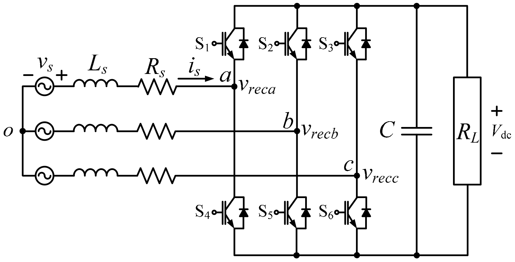
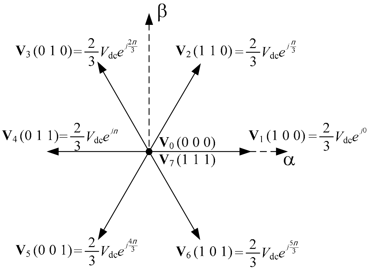
2. Conventional Finite Predictive Current Control Method Using Two-Vector For Three-Phase Rectifier

The main circuit of the three-phase rectifier is shown in Figure 1. The three-phase rectifier in Figure 1 is composed of the six power transistors, the three-phase supply voltages v s , the input inductances L s , and the input resistances R s at its input side. By the circuit structure, the supply voltage vector is described as:
v s = R s i s + L s d i s d t + v r e c
where i s and v r e c are the source current vector and the rectifier input voltag vector.
Using constant sampling period, the derivative of the current can be approximated in discrete-time domain as:
d i s d t i s k + 1 T s i s k T s T s
where i s k + 1 T s and i s k T s are source current vectors at k + 1 th and k th instant, respectively, and T s is the sampling period. In the discrete-time domain, the future source current vector at k + 1 th instant can be predicted using (1) and (2) as:
i s k + 1 T s = i s k T s + T s L s v s k T s v r e c k R s i s k T s
Therefore, the future source current will be changed according to the rectifier input voltage vector shown in Figure 2.
For applying two voltage vectors at each sampling period, sampling period T s can be divided into two time intervals according to the selected rectifier input voltage vector and it can be described as:
T s = T 1 + T 2
where T 1 and T 2 are time intervals of first applied voltage vector v r e c 1 k and second applied voltage vector v r e c 2 k , respectively. The future source current in Algorithm (3) can be expressed using two voltage vectors and two time intervals as:
i s k + 1 T s = i s k T s + T 1 k L s v s k T s v r e c 1 k R s i s k T s
+ T 2 k L s v s k T s + T 1 k v r e c 2 k R s i s k T s + T 1 k
In selecting two optimal rectifier input voltage vectors to minimize the error between the real source currents and the reference source currents in the cost function, predicted future currents need to be calculated. The rectifier input voltage vectors, v r e c 1 k and v r e c 2 k , are decided among seven voltage vectors except for one zero voltage vector between V 0 and V 7 , respectively. Therefore, 49 voltage vector sets can be considered and computation time needs to be compensated. For the delay compensation, by shifting Algorithm (5) one-instant forward, the future source current at the k + 2 th instant is obtained as:
i s k + 2 T s = i s k + 1 T s + T 1 k + 1 L s v s k + 1 T s v r e c 1 k + 1 R s i s k + 1 T s
+ T 2 k + 1 L s v s k + 1 T s + T 1 k + 1 v r e c 2 k + 1 R s i s k + 1 T s + T 1 k + 1
Compared with the fast sampling frequency, the source voltage changes at a much lower frequency (60 Hz), and thus, the future source voltage can be estimated as:
v s k T s v s k T s + T 1 k v s k + 1 T s
The cost function for two rectifier input voltage vectors is defined as:
G = i s α * k + 2 T s i s α k + 2 T s 2 + i s β * k + 2 T s i s β k + 2 T s 2
+ i s α * k + 1 T s + T 1 k + 1 i s α k + 1 T s + T 1 k + 1 2
+ i s β * k + 1 T s + T 1 k + 1 i s β k + 1 T s + T 1 k + 1 2
Applying Algorithms (6), (8), (12), (13), and (14) to (8), the cost function in Algorithm (8) can be presented for T 1 k + 1 . Then, by differentiating Algorithm (8) from T 1 k + 1 , the optimal time interval to divide two rectifier input voltage vectors can be calculated as:
G T 1 k + 1 = 0
The time interval of the first applied rectifier input voltage vector v r e c 1 k + 1 in each set can be calculted by solving Algorithm (9) as:
T 1 k + 1 = V d α L s E 2 α + T s V d α V L α + V d β L s E 2 β + T s V d β V L β L s E 1 α L s T s I d α * V L α + E 1 β L s T s I d β * V L β V d α 2 + V d β 2 + L s T s I d α * V L α 2 + L s T s I d β * V L β 2
where V d m = v r e c 1 m k + 1 v r e c 2 m k + 1 ,
V L m = v s m k + 1 T s R s i s m k + 1 T s v r e c 1 m k + 1 ,
E 1 m = i s m * k + 1 T s i s m k + 1 T s ,
E 2 m = i s m * k + 2 T s i s m k + 2 T s ,
I d m * = i s m * k + 2 T s i s m * k + 1 T s and m = α, β.
The time interval of the second applied rectifier input voltage vector v r e c 2 k + 1 can be calculated as:
T 2 k + 1 = T s T 1 k + 1
The reference source currents at k + 2 th instant can be calculated by using the Lagrange extrapolation as:
i s * k + 2 T s = 3 i s * k + 1 T s 3 i s * k T s + i s * k 1 T s
The reference source currents at k + 1 T s + T 1 th instant can be calculated as:
i s * k + 1 T s + T 1 k + 1 = i s * k + 1 T s + T 1 k + 1 T s i s * k + 2 T s i s * k + 1 T s
The future source currents at k + 1 T s + T 1 th instant can be calculated as:
i s k + 1 T s + T 1 k + 1 = i s k + 1 T s + T 1 k + 1 L s v s k + 1 T s v r e c 1 k + 1 R s i s k + 1 T s

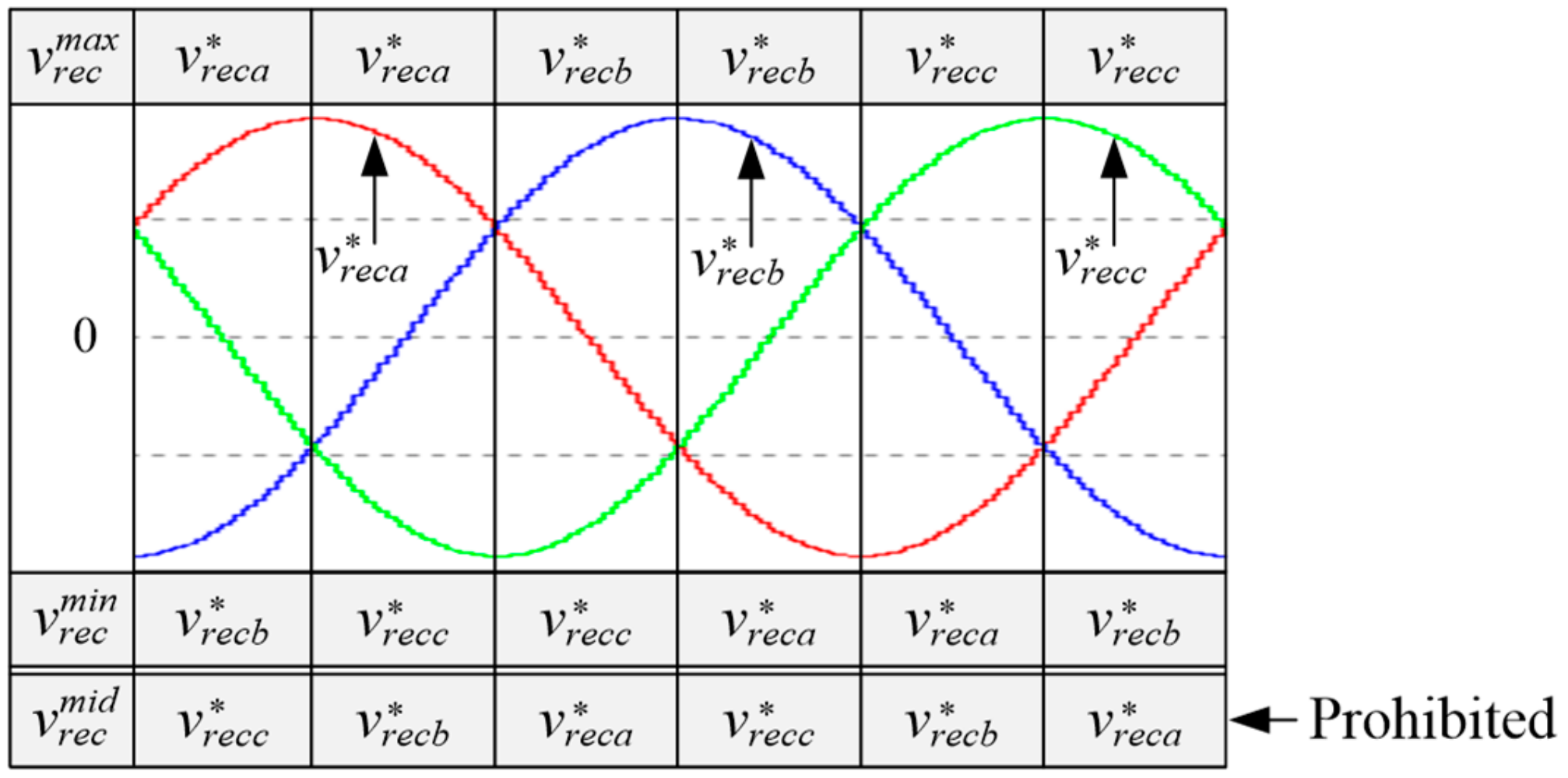
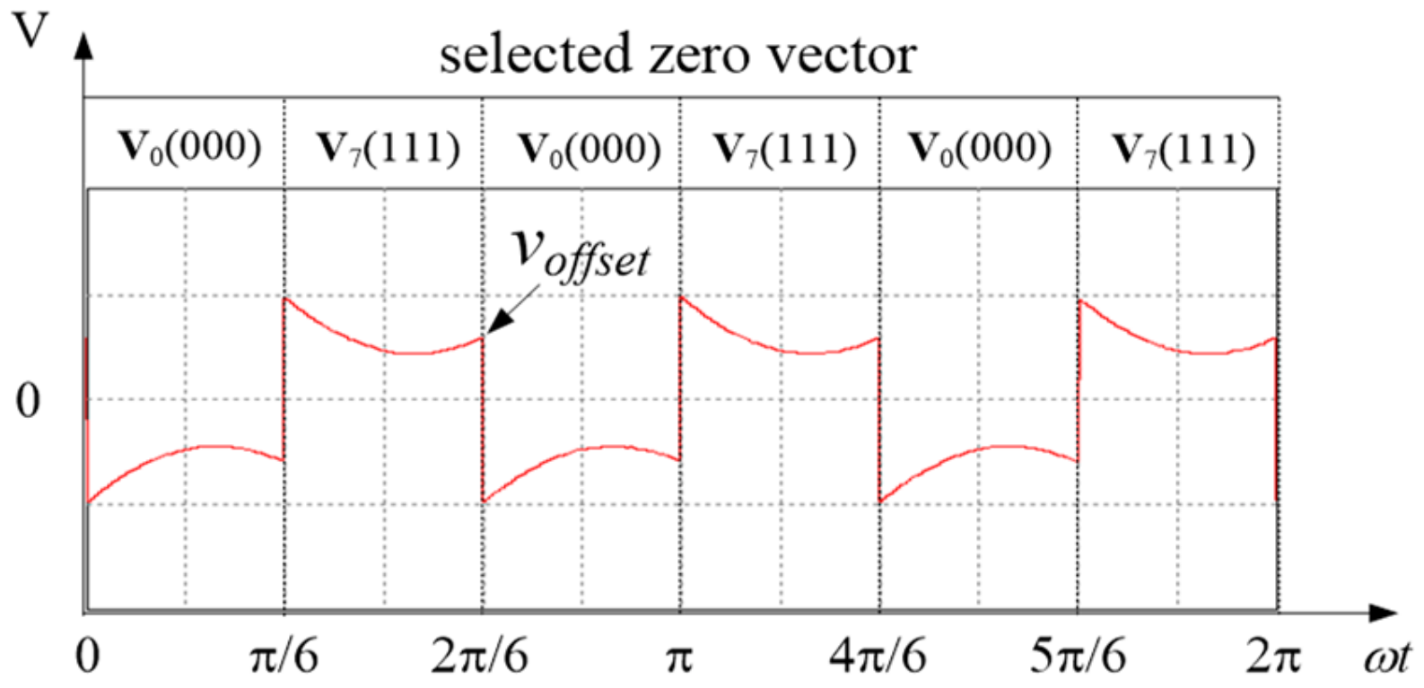
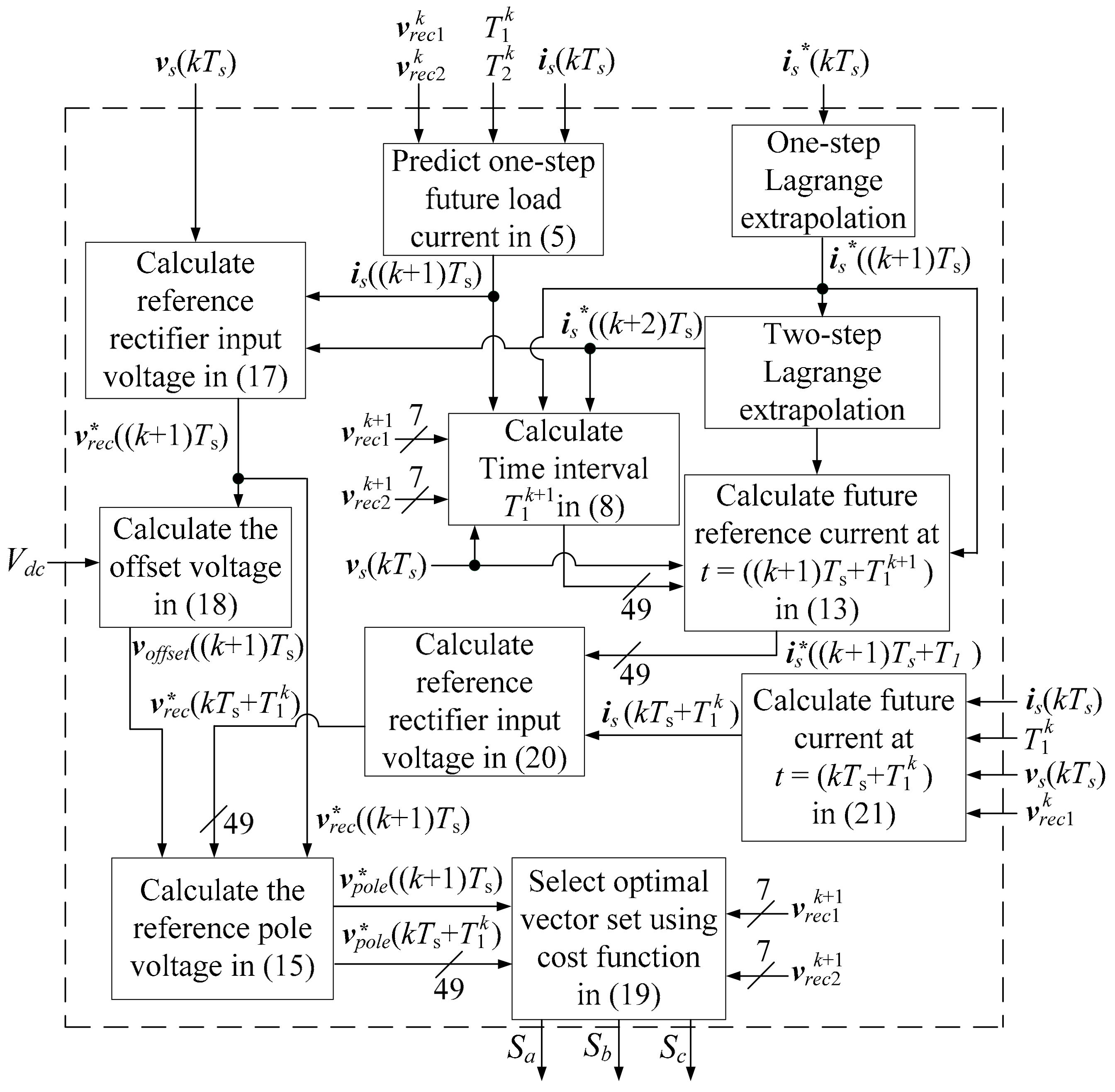
3. Proposed Switching Loss Reduction Strategy for Three-Phase Rectifier Using Two-Vector Based on Offset Voltage Injection

The switching losses of the rectifier are dependent on absolute values of the source currents flowing through the switches at switching instant, and therefore the switching losses can be reduced by stopping the operation of the switch flowing the largest source current among the rectifier switches. In the proposed method, the offset voltage is calculated and injected into the reference rectifier input voltages to clamp one leg conducting the largest source current among three legs to either the positive output voltage or the negative output voltage. In the rectifier system, the reference pole voltages of the rectifier ( v p o l e * ), the reference rectifier input voltages ( v r e c * ), and the offset voltage ( v o f f s e t k + 1 T s ) can be written as:
v p o l e * k + 1 T s = v r e c * k + 1 T s + v o f f s e t k + 1 T s
The rectifier input voltages are acquired by shifting Algorithm (3) one-instant forward as:
v r e c   k + 1 T s = v s k + 1 T s R s i s k + 1 T s L s i s k + 2 T s i s k + 1 T s T s
The reference rectifier input voltages at k + 1 th instant are obtained by the replacing future source current i s k + 2 T s with the reference source current i s * k + 2 T s as:
v r e c * k + 1 T s = v s k + 1 T s R s i s k + 1 T s L s i s * k + 2 T s i s k + 1 T s T s
The reference source current i s * k + 2 T s and predicted source current i s k + 1 T s can be obtained by using Algorithms (12) and (5), respectively. The three-phase reference rectifier input voltages obtained by Algorithm (17) are classified as v r e c m a x k + 1 T s , v r e c m i d k + 1 T s , and v r e c m i n k + 1 T s according to the magnitude of each phase reference rectifier input voltage, as shown in Figure 3. To assure a linear modulation range, the prohibitive phase that should not be clamped, corresponds to the phase with the reference rectifier input voltage v r e c m i d k + 1 T s , which has the medium amplitude value among the three rectifier voltages.
Thus, except for v r e c m i d k + 1 T s , one of the two rectifier legs with v r e c m a x k + 1 T s and v r e c m i n k + 1 T s has to be clamped to either the positive output voltage or the negative output voltage through the comparison of absolute value of the two rectifier input currents. To find the larger source current, the input currents of the rectifier associated with v r e c m a x k + 1 T s and v r e c m i n k + 1 T s are assigned to i r e c m a x k + 1 T s and i r e c m i n k + 1 T s , respectively. When the rectifier input currents and the reference rectifier input voltages are assigned, the offset voltage can be determined as:
i f   i r e c m a x k + 1 T s > i r e c m i n k + 1 T s v o f f s e t k + 1 T s = V d c 2 v r e c m a x k + 1 T s i f   i r e c m a x k + 1 T s < i r e c m i n k + 1 T s v o f f s e t k + 1 T s = V d c 2 v r e c m i n k + 1 T s
The rectifier input voltages according to the switching states are shown in Table 1.
In the proposed method, the cost function is defined to minimize the error between the reference rectifier input voltages and the real rectifier input voltage as:
G = v p o l e α * k + 1 T s v r e c 2 α k + 1 2 + v p o l e β * k + 1 T s v r e c 2 β k + 1 2
+ v p o l e α * k T s + T 1 v r e c 1 α k + 1 2 + v p o l e β * k T s + T 1 v r e c 1 β k + 1 2
where v r e c 1 α β k + 1 and v r e c 2 α β k + 1 are the first and second rectifier input voltages, which are decided according to the switching states, as shown in Table 1. The time interval of first rectifier input voltage vector T 1 k + 1 can be obtained by using Algorithm (10). The reference rectifier input voltages at k T s + T 1 k th instant can be calculated by changing the time in Algorithm (17) from k + 1 T s th to k T s + T 1 k th as:
v r e c * k T s + T 1 k = v s k T s + T 1 k R s i s k T s + T 1 k L s i s * k + 1 T s + T 1 k + 1 i s k T s + T 1 k T s
The reference source current, i s * k + 1 T s + T 1 k + 1 , can be obtained by using Algorithm (13). The predicted source current, i s k T s + T 1 k , can be calculated as:
i s k T s + T 1 k = i s k T s + T 1 k L s v s k T s v r e c 1 k R s i s k T s
The cost function of the proposed method in Algorithm (19) selects an optimal switching status that can make source current component closet to the future references among the 49 possible voltage vector sets.
The reference rectifier input voltages are modified by the offset voltage to clamp the one leg with the largest source currents, so the proposed algorithm can reduce the switching losses and make the real source currents track the reference source currents. The proposed algorithm has to select the appropriate one zero vector to maintain the clamping period, though the zero vectors, V7 and V0, generated by the rectifier, have the same voltage value as each other. In the proposed method, one of the zero voltage vectors between V7 and V0 is selected as the optimal zero voltage vector by detecting the polarity of the offset voltage, as shown in Figure 4.
Zero vectors V7 and V0 are selected when the offset voltage v o f f s e t k + 1 T s is positive and negative, respectively. Zero voltage vector selection makes it possible to maintain the clamping period. Figure 5 shows the entire control scheme of the proposed method. In the proposed method, the offset voltage is calculated from the reference rectifier input voltages and the output voltage in every sampling period, so the clamping regions are suitably changed. Thus, the proposed algorithm can reduce the switching losses at both transient-state and steady-state.

4. Simulation and Experimental Results

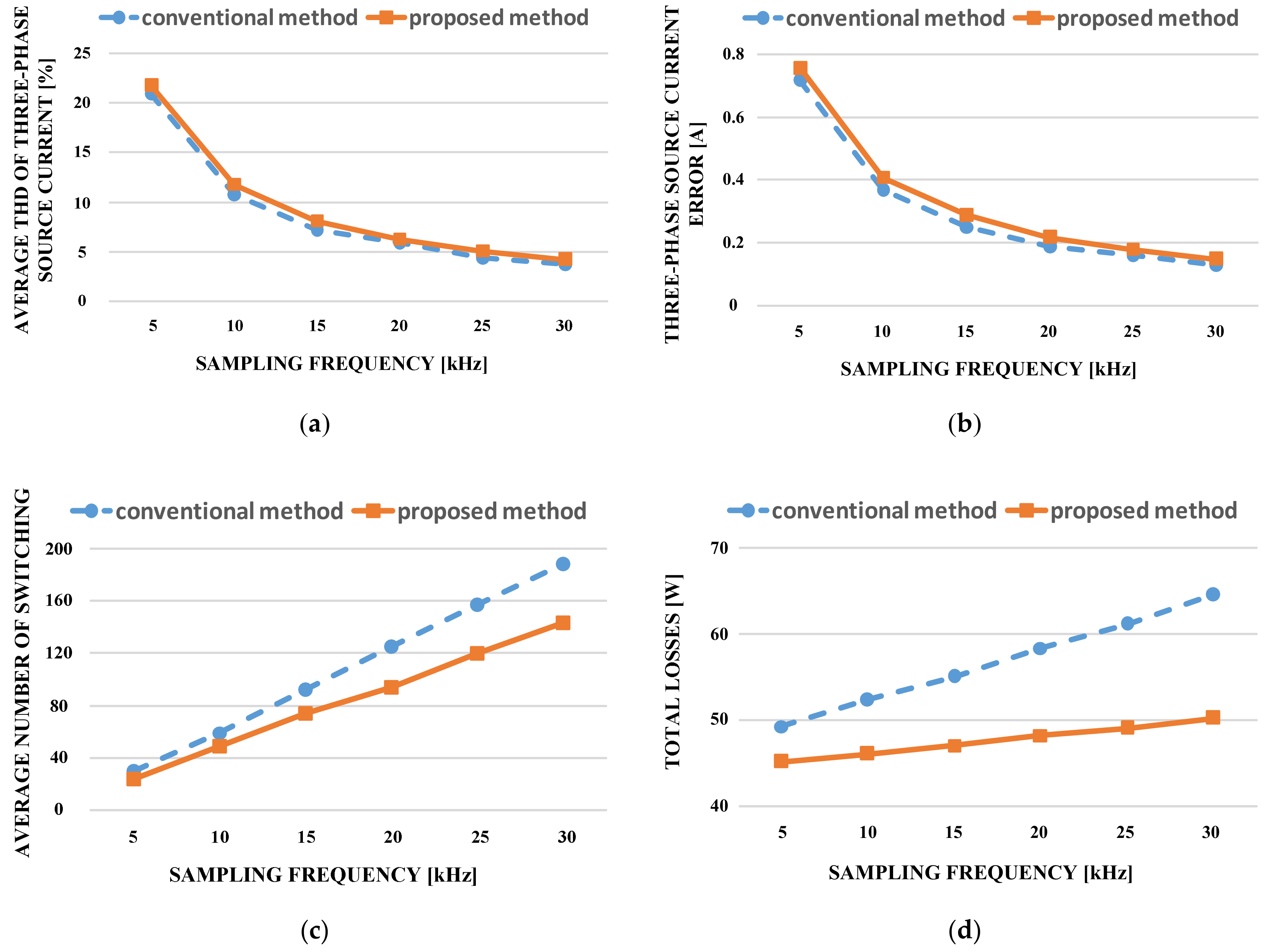
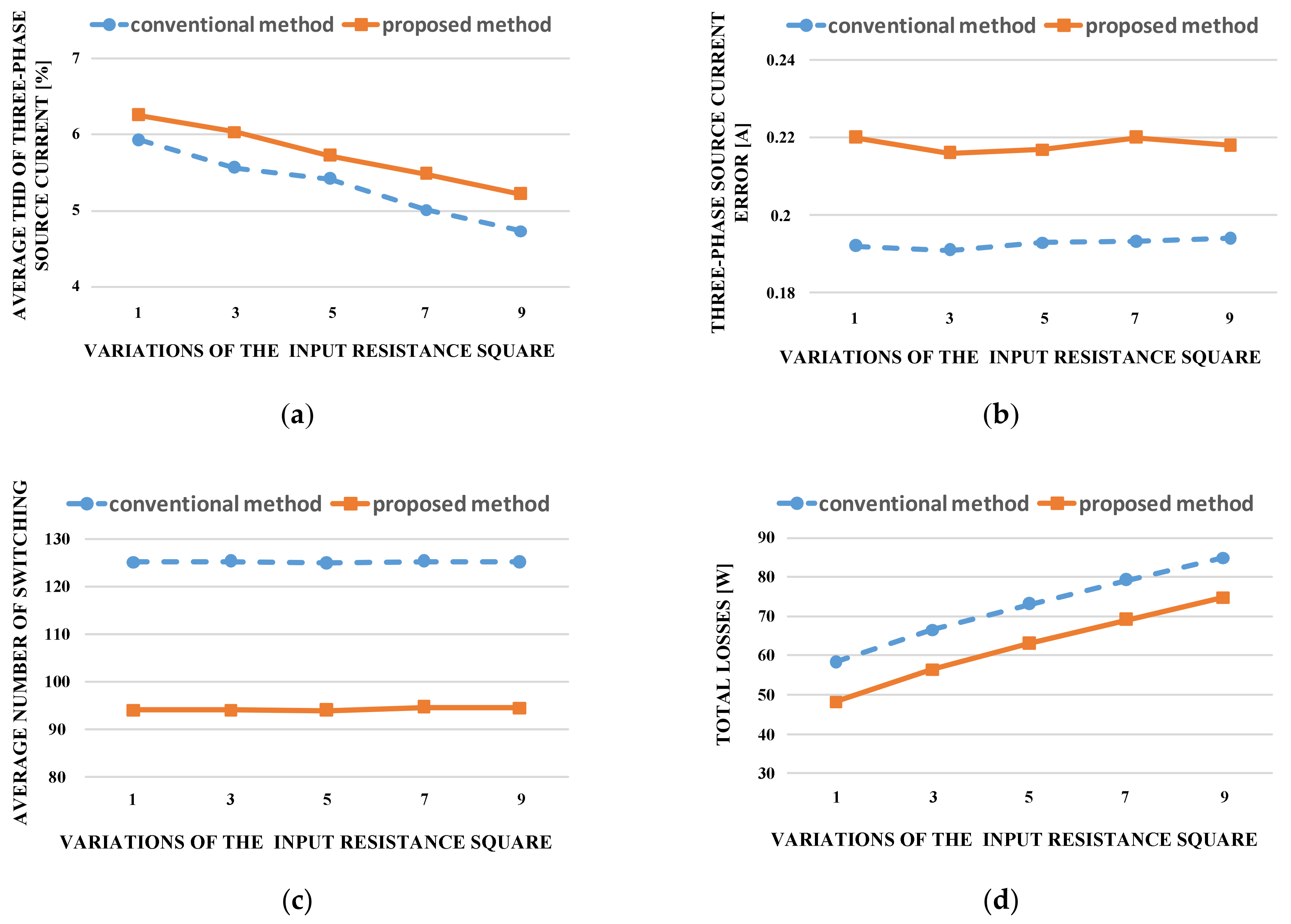
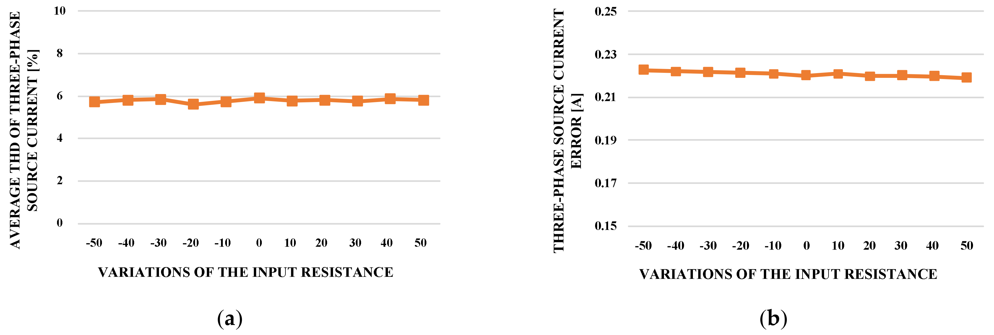
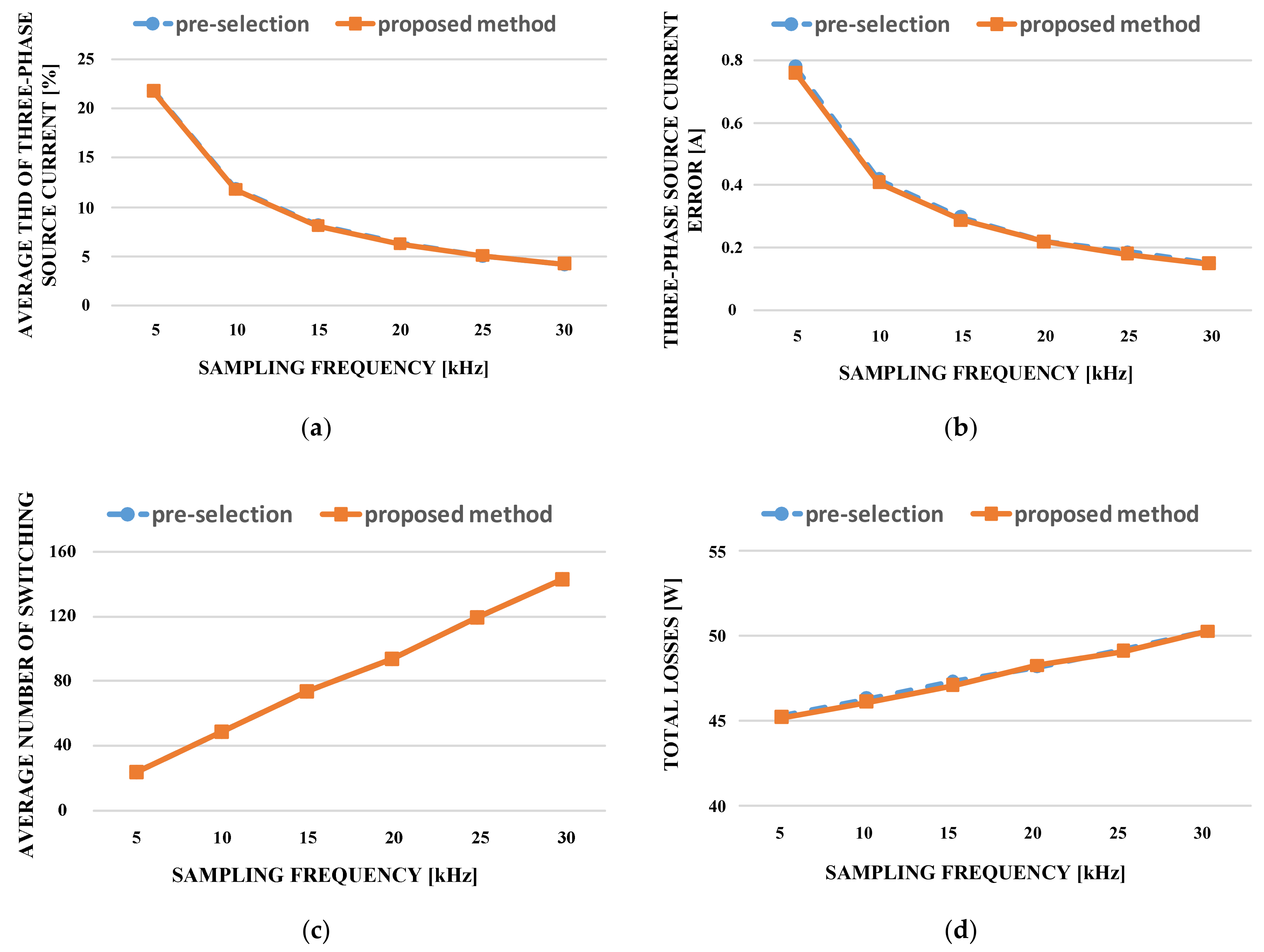
4.1. Simulation Results

A simulation and experiment were conducted to prove the validity of the proposed algorithm. The parameters used in simulation and experiment are as follows: Peak value of source voltage v s = 100 V , reference output voltage V d c * = 250 V , input inductance L s = 10 mH , input resistance R s = 1   Ω, R l o a d = 100 Ω, output capacitance C = 550 nF, and sampling frequency f s = 20 kHz . Figure 6 shows the three-phase source currents, the a-phase source voltage, and a-phase upper switch. Figure 6a,b show the waveform of the conventional method and the proposed method, respectively. It can be seen that in both control methods, the three-phase source currents are sinusoidal waveforms and also in phase with the source voltages. The conventional method uses the zero state V0 between the zero states of the rectifier V0 and V7, which is illustrated with the switching pattern of S1. The a-phase upper switch waveform is clamped to the negative output voltage. On the other hand, the usage of the zero state V7 leads to clamping of the a-phase waveform to the positive output voltage. The switching waveform of S1 shows that the proposed algorithm inhibits the switch S1 from commutating around the peak input current due to the rectifier voltage modified by the offset voltage injection.
Figure 7a,b show the FFT (fast Fourier transform) of the conventional method and the proposed method, respectively. As can be seen, the THD of the proposed method was slightly higher than that of the conventional method, but it did not effect the control performance.
Figure 8a,b show the output voltage of the conventional method and the proposed method, respectively. As shown in Figure 9, the output voltages of both control algorithms are controlled at 250 V.
Figure 9 shows the transient response of the conventional algorithm and the proposed algorithm. Since the magnitude of the reference source current is the output of the PI controller, it is greatly affected by the PI gain of the PI controller. Therefore, in order to remove the influence of PI gain, magnitude of the reference was manually converted. As shown in Figure 9, the magnitude of the reference source currents varied from 3 A to 5 A. It can be seen that the transient response rates of the two control methods are the same because they select the same vectors when the PI controller was removed.

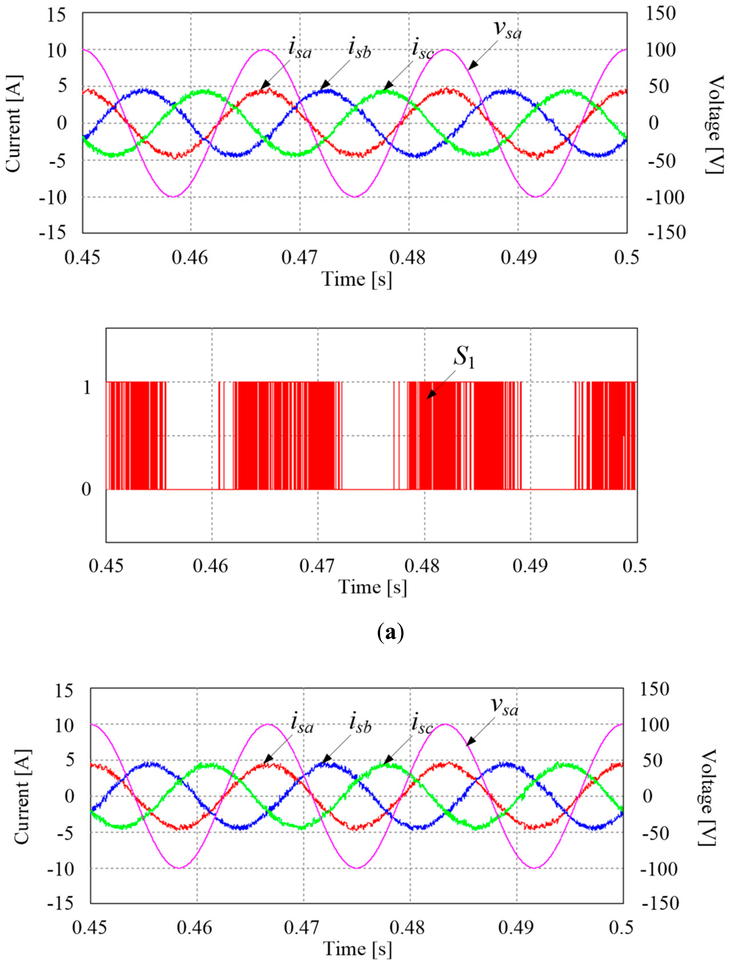
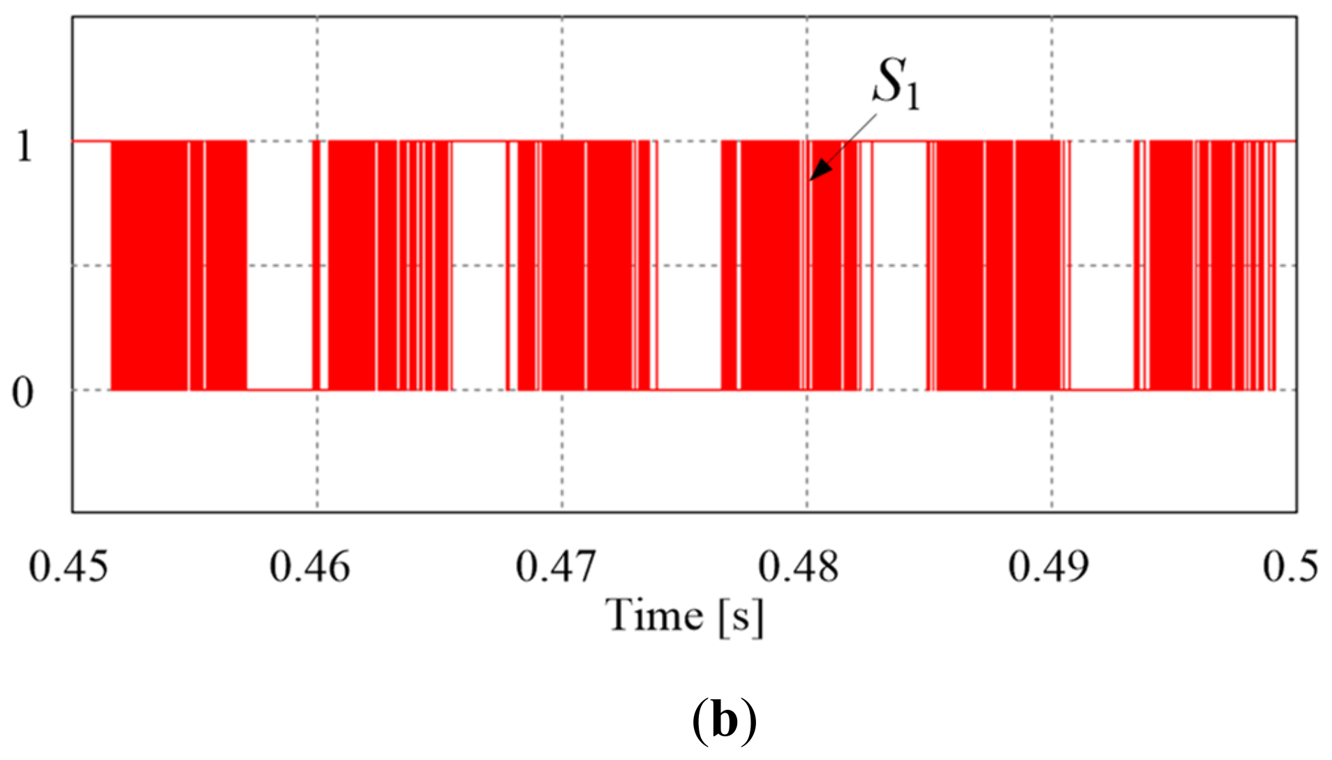
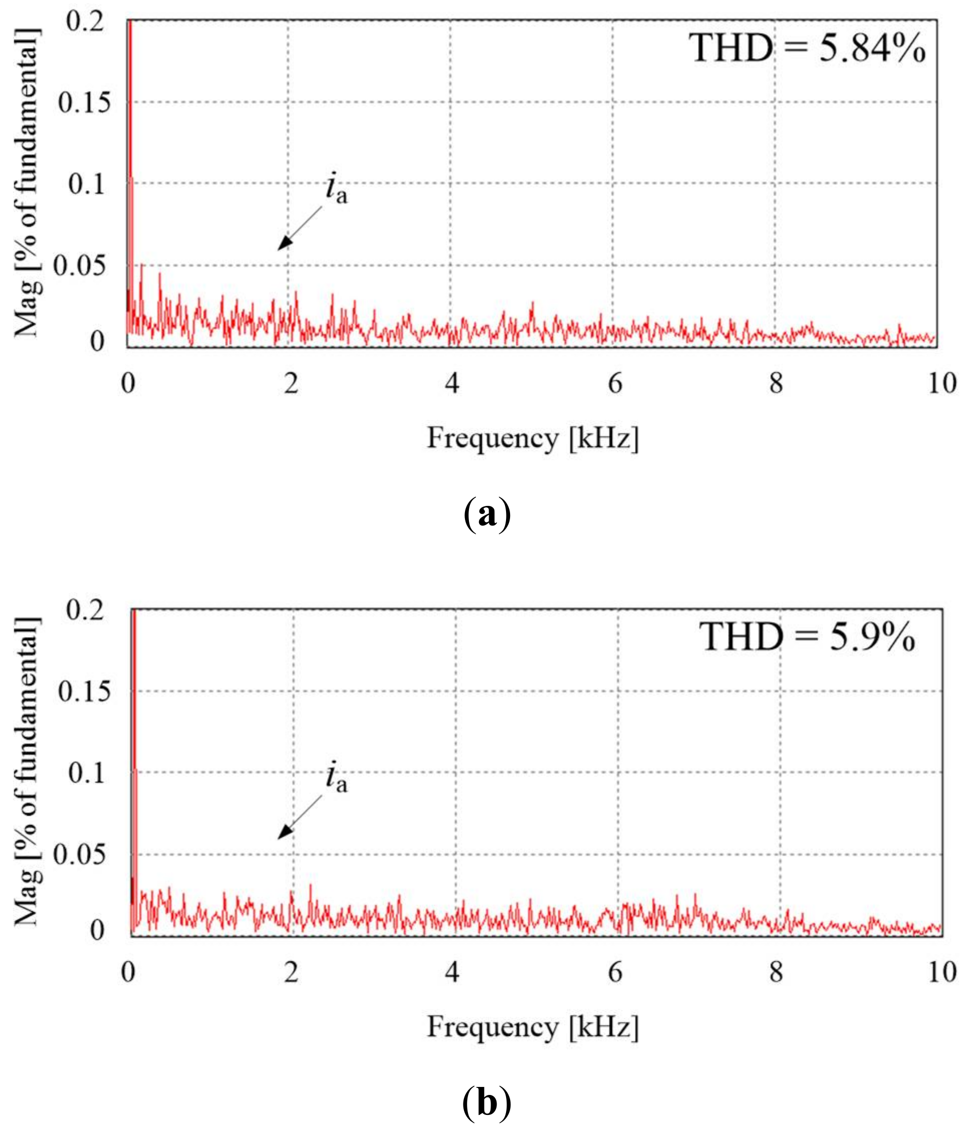
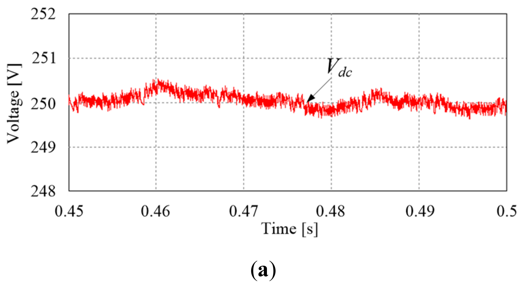
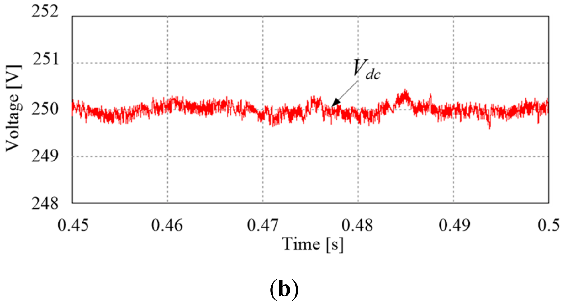
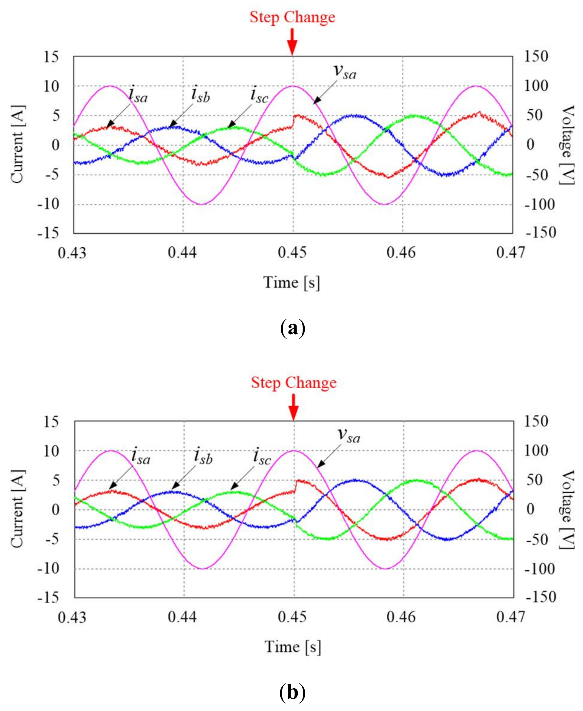
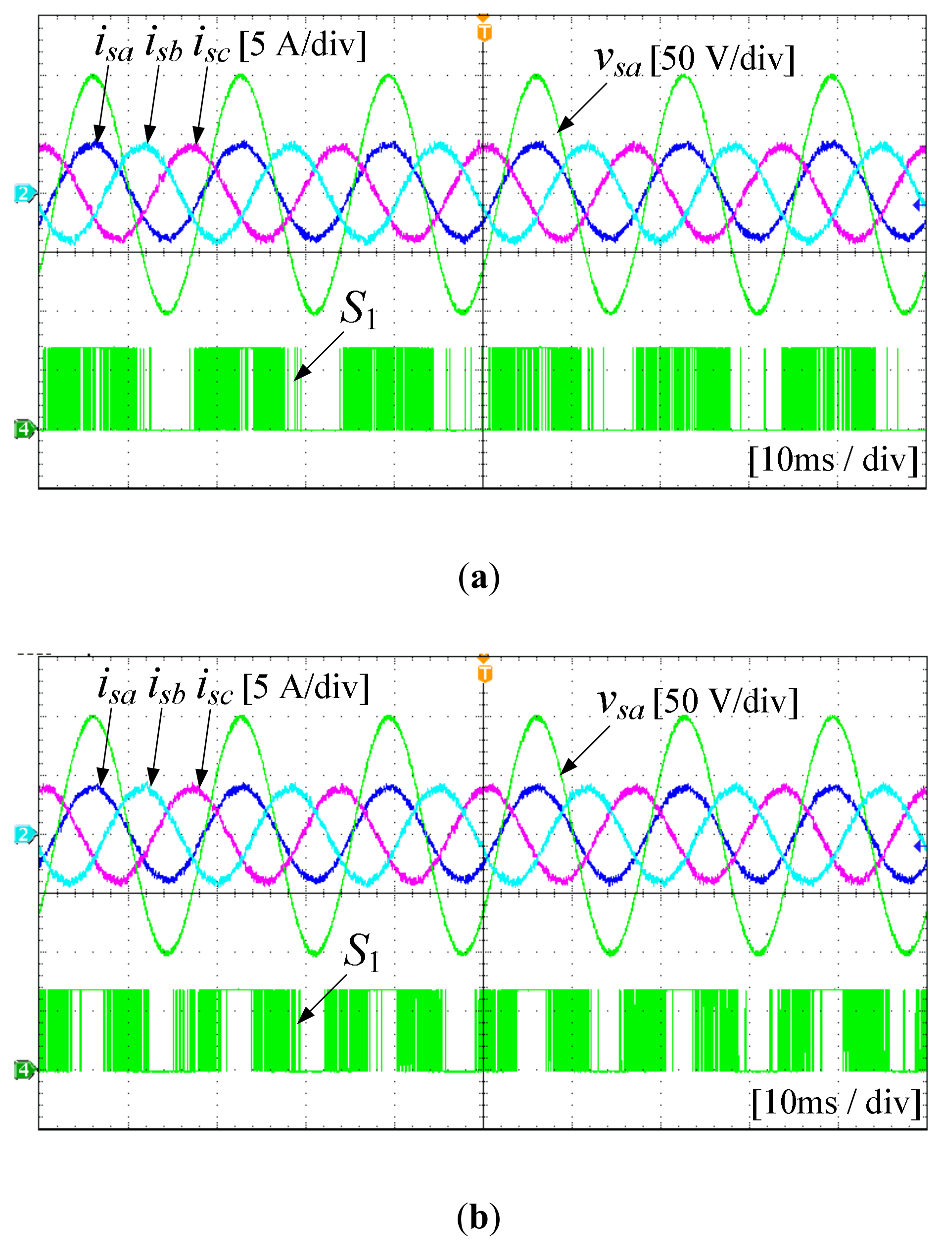
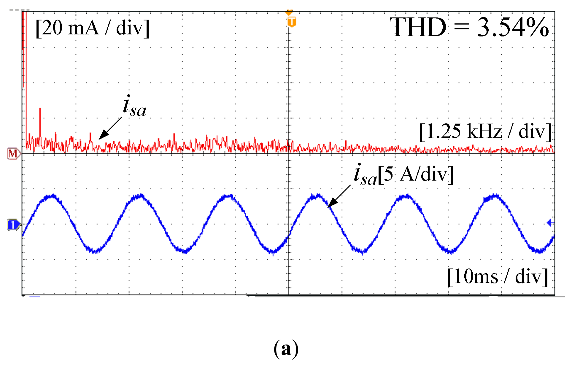
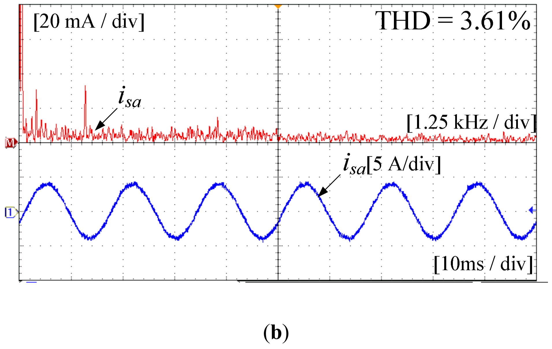
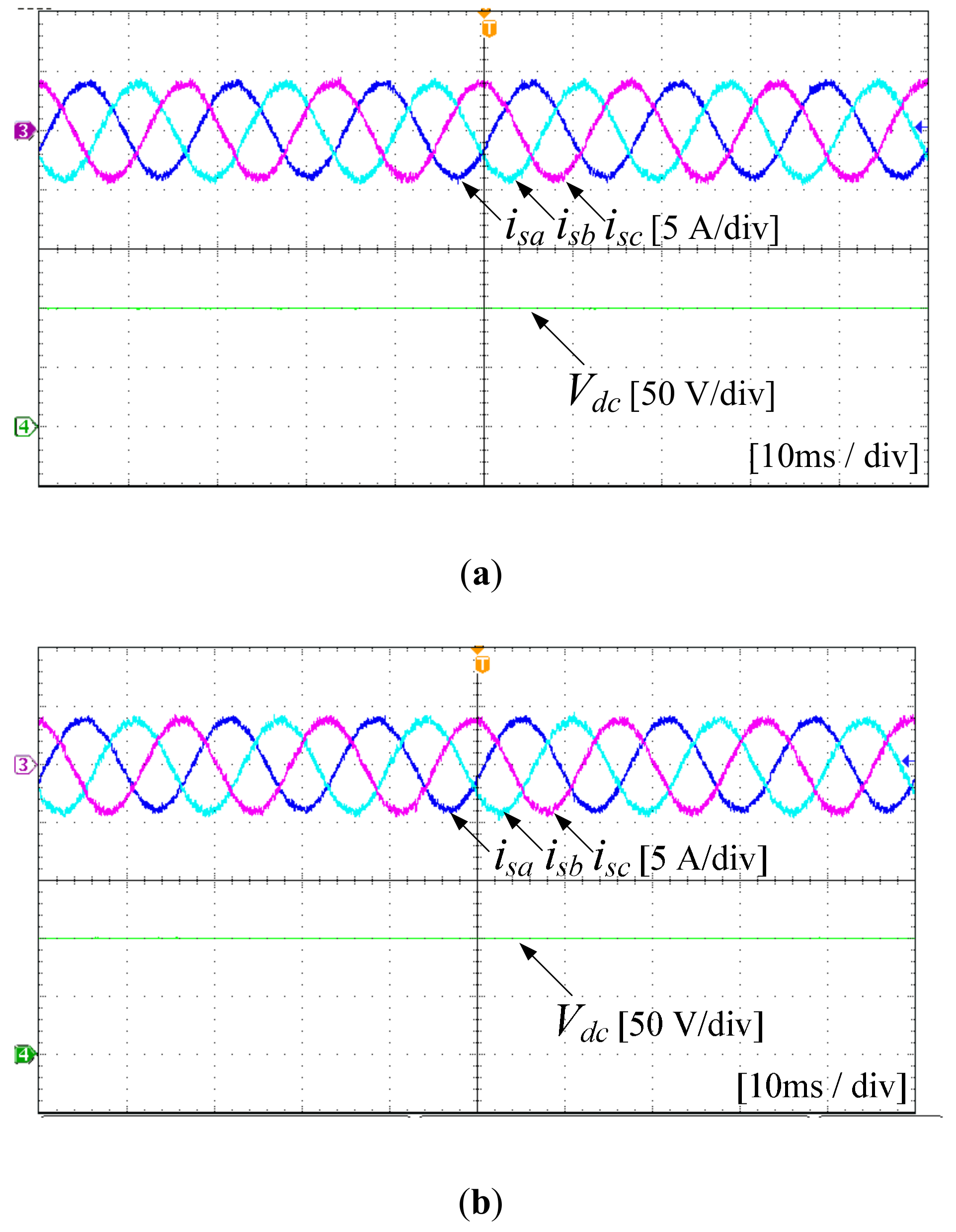
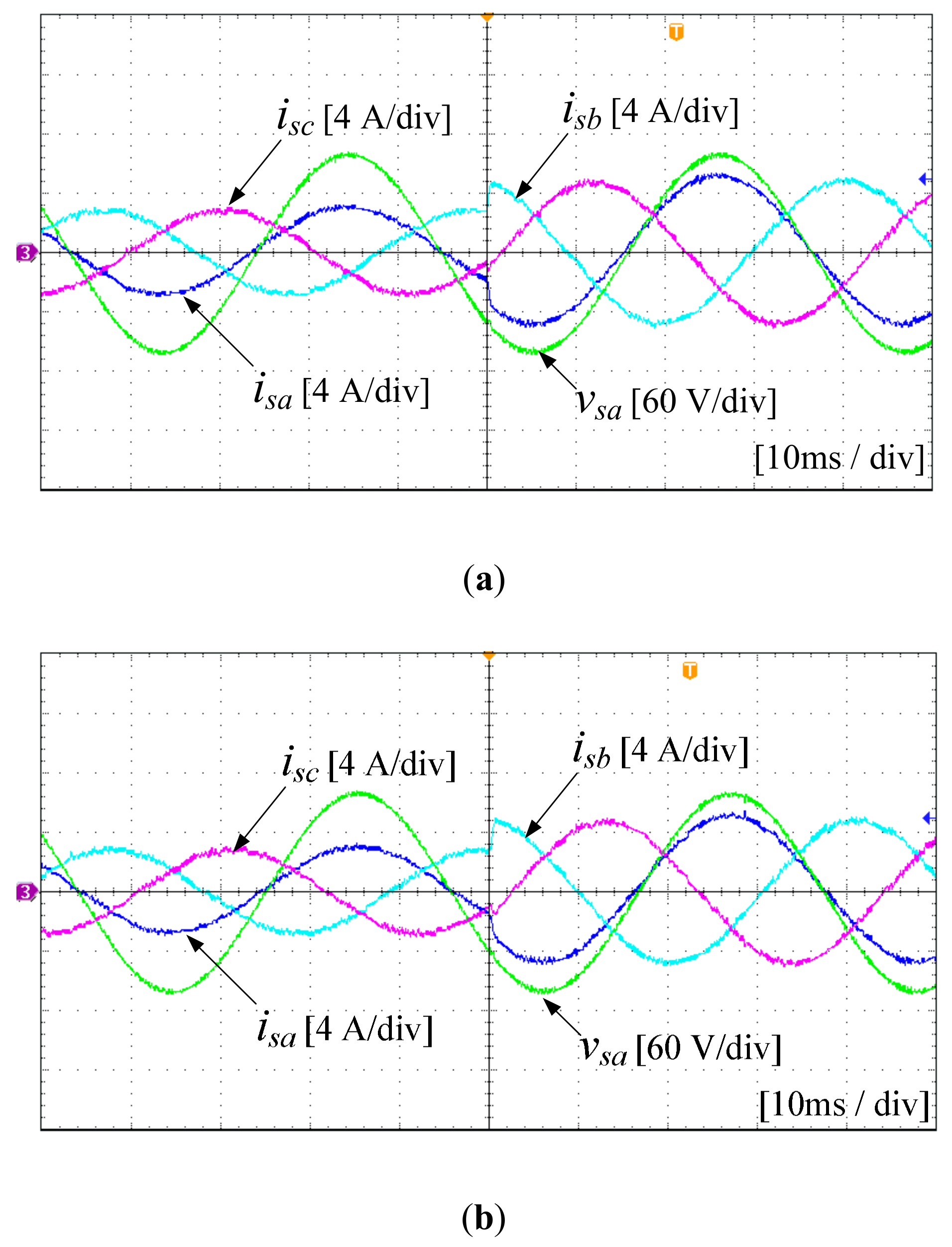
4.2. Experimental Results

Figure 10 shows the waveforms of three-phase source currents, a-phase source voltage, and a-phase upper switch obtained from the experiment. Figure 10a,b show the experimental results of the conventional method and the proposed method, respectively. As shown in Figure 11, the three-phase source currents are sinusoidal waveforms and are also in phase with the source voltages in both the control methods. Additionally, clamping regions of two control methods are the same as the simulation results in Figure 6. In the conventional method, the a-phase upper switch waveform is only clamped to the negative output voltage because the conventional method only uses the zero state V0 between the zero states of the rectifier V0 and V7. However, the a-phase upper switch of the proposed method is clamped to the positive output voltage and the negative output voltage. It makes the rectifier reduce the switching losses.
Figure 11a,b show the experimental results of FFT (fast Fourier transform) of the a-phase source current obtained from the the conventional method and the proposed method, respectively. As can be seen, similar to the previous simulation results in Figure 7, the proposed method has a slightly higher THD than the conventional method.
Figure 12 shows the experimental waveforms of the three-phase source currents and the output voltage. Figure 12a,b show the waveforms obtained from the conventional method and the proposed method, respectively. As shown in Figure 12, the output voltages of both control methods are controlled at 250 V.
Figure 13 shows the experimental waveforms of the transient response of the conventional method and the proposed method. The experiment was also performed without a PI controller, like the simulation in Figure 9. The magnitude of the reference varied from 3 A to 5 A. It can be seen that the transient response rate is the same to the previous simulation results in Figure 9.

5. Performance Comparison

To show the effectiveness of the proposed algorithm, the performance comparisons of the THD percentage of the source current, current error, total loss, and number of switching between the proposed algorithm and the conventional algorithm were conducted. Figure 14a–d show the average THD of three-phase source current, three-phase source current error, average number of switching, and total losses, respectively. As shown in Figure 14a,b, average THD of the three-phase source current and the three-phase source current error of the proposed method are slightly higher than those of the conventional method. However, as sampling frequency increases, the difference in the average number of switching between the proposed algorithm and conventional algorithm also increases, and the number of switching of the proposed method is much lower than that of the conventional method. This is because the proposed method clamps one leg with the largest source current to reduce the switching losses. Additionally, the total losses of the proposed algorithm is much lower than those of the conventional algorithm, as shown in Figure 14d. This is because the switching losses of the proposed method have been reduced by the reduced number of switching, as shown in Figure 14c.
Table 2 shows the average THD of three-phase source current, three-phase source current error, average number of switching, and total losses when the switching frequency is 20 kHz. As shown in the table, the average THD of the three-phase source current and three-phase source current error are slightly worse than the conventional method. However, the number of switching of the proposed method is reduced by 25% compared to the number of switching of the conventional method, and the total losses of the proposed method are about 8% less than that of the conventional method.
Figure 15 shows the results of the performance comparison according to the variation of the input resistance square. As shown in the figure, the average THD of the three-phase source current decreases as the value of the input resistance square increases. Furthermore, the total losses increase as the value of the input resistance square increases. However, the variation of the input resistance square does not affect the current error and average number of switching. In addition, it is shown that the proposed method yields smaller average numbers of switchings and lower losses than the conventional method, at the expense of slightly increased THD values and current errors.
Performance of the model predictive control methods is generally affected by the model accuracy. The effects of errors in the input resistance and the input inductance on average THD of three-phase source current and current error obtained from the proposed method are compared in Figure 16. Figure 16a–d show the effects of errors in the input resistance and inductance. As shown in Figure 16a,b, the uncertainty of the input resistance does not affect the performance of the source currents in the proposed method. Additionally, the uncertainty of the input inductance does not affect the average THD of the three-phase source current. However, underestimations and overestimations in the input inductance were found to slightly degrade the current error for the proposed method.
A similar study that has been conducted previously was on the pre-selection technique [27]. This control method uses four available vectors with one switch, which are classified by the vector pre-selection method clamping one leg and conducting the largest current among the three legs to reduce the switching losses. Figure 17 shows the performance comparison between the pre-selection algorithm and the proposed algorithm. Figure 17a–d show the average THD of three-phase source current, three-phase source current error, average number of switching, and total losses, respectively. As both algorithms clamp the switch with the largest current flow, the performance of the two control methods is almost the same.

6. Conclusions

In this paper, the MPC algorithm with the offset voltage injection to reduce switching losses was proposed. The proposed algorithm calculates the offset voltage to stop the switching operation of one leg with the largest source current among the three legs in the rectifier by clamping the leg to either the positive output voltage or negative output voltage in every sampling period. As a result, the offset voltage injection makes the rectifier use both zero state V 0 and V 7 . It makes the rectifier reduce the switching losses. In addition, the proposed method also applies the two-vector technique to make the source current with a lower THD (total harmonic distortion). Compared to the conventionall method, the THD and current error of the proposed method are slightly higher than those of the conventional method. However, the number of switching and total losses of the proposed method are reduced by 25% and 8% compared to those of the conventional method with the sampling frequency f s = 20 kHz . The number of switching is reduced because the switches are clamped. Additionally, the switching losses of the total losses is reduced because the number of switching is reduced at the high current region. A simulation and experiment were conducted in order to verify the effectiveness of the proposed algorithm.

Author Contributions

E.J. and S.K. conceived and designed the experiments; E.J. performed the experiments; E.J. and S.K. analyzed the data; S.K. contributed reagents/materials/analysis tools; E.J. and S.K. wrote the paper.

Funding

This research was supported by the National Research Foundation of Korea (NRF) grant funded by the Korean government (MSIP) (2017R1A2B4011444) and the Human Resources Development (No.20174030201810) of the Korea Institute of Energy Technology Evaluation and Planning (KETEP) grant funded by the Korea government Ministry of Trade, Industry and Energy.

Acknowledgments

This research was supported by the National Research Foundation of Korea (NRF) grant funded by the Korean government (MSIP) (2017R1A2B4011444) and the Human Resources Development (No.20174030201810) of the Korea Institute of Energy Technology Evaluation and Planning (KETEP) grant funded by the Korea government Ministry of Trade, Industry and Energy.

Conflicts of Interest

The authors declare no conflict of interest.

References

  1. Nene, H.; Zaitsu, T. Bi-Directional PSFB DC-DC Converter with Unique PWM Control Schemes and Seamless Mode Transitions Using Enhanced Digital Control. In Proceedings of the IEEE Applied Power Electronics Conference and Exposition (APEC), Tampa, FL, USA, 26–30 March 2017; pp. 3229–3233. [Google Scholar]
  2. Fuchs, S.; Beck, S.; Biela, J. Analysis and Reduction of the Output Voltage Error of PWM for Modular Multilevel Converters. IEEE Trans. Ind. Electron. 2019, 66, 2291–2301. [Google Scholar] [CrossRef]
  3. Padhee, V.; Sahoo, A.K.; Mohan, N. Modulation Techniques for Enhanced Reduction in Common-Mode Voltage and Output Voltage Distortion in Indirect Matrix Converters. IEEE Trans. Power Electron. 2017, 32, 8655–8670. [Google Scholar] [CrossRef]
  4. Foti, S.; Testa, A.; Scelba, G.; Sabatini, V.; Lidozzi, A.; Solero, L. A Low THD Three-Level Rectifier For Gen-Set Applications. IEEE Trans. Ind. Appl. 2019, 55, 6150–6160. [Google Scholar] [CrossRef]
  5. Kwak, S.; Toliyat, H.A. Design and rating comparisons of PWM voltage source rectifiers and active power filters for AC drives with unity power factor. IEEE Trans. Power Electron. 2005, 20, 1133–1142. [Google Scholar] [CrossRef]
  6. Kwak, S.; Toliyat, H.A. Design and performance comparisons of two multi-drive systems with unity power factor. IEEE Trans. Power Deliv. 2005, 20, 417–426. [Google Scholar]
  7. Wai, R.; Yang, Y. Design of Backstepping Direct Power Control for Three-Phase PWM Rectifier. IEEE Trans. Ind. Appl. 2019, 55, 3160–3173. [Google Scholar] [CrossRef]
  8. Habetler, T.G. A space vector based rectifier regulator for AC/DC/AC converters. IEEE Trans. Power Electron. 1993, 8, 3–36. [Google Scholar] [CrossRef]
  9. Restrepo, J.; Aller, J.; Viola, J.; Bueno, A.; Habetler, T. Optimum space vector computation technique for direct power control. IEEE Trans. Power Electron. 2009, 24, 1637–1645. [Google Scholar] [CrossRef]
  10. Liu, J.; Gong, C.; Han, Z.; Yu, H. IPMSM Model Predictive Control in Flux-Weakening Operation Using an Improved Algorithm. IEEE Trans. Ind. Electron. 2018, 65, 9378–9387. [Google Scholar] [CrossRef]
  11. Kubasiak, N. Model Predictive Control of Transistor Pulse Converter for Feeding Electromagnetic Valve Actuator with Energy Storage. In Proceedings of the 44th IEEE Conference on Decision and Control, Seville, Spain, 15 December 2005; pp. 6794–6799. [Google Scholar]
  12. Mercorelli, P.; Kubasiak, N.; Liu, S. Multilevel Bridge Governor by Using Model Predictive Control in Wavelet Packets for Tracking Trajectories. In Proceedings of the IEEE 2004 International Conference on Robotics and Automation, (ICRA ’04), New Orleans, LA, USA, 26 April–1 May 2004; Volume 4, pp. 4079–4084. [Google Scholar]
  13. Mercorelli, P. A Multilevel Inverter Bridge Control Structure with Energy Storage Using Model Predictive Control for Flat Systems. J. Eng. 2013, 2013, 750190. [Google Scholar] [CrossRef]
  14. Gardezi, M.S.M.; Hasan, A. Machine Learning Based Adaptive Prediction Horizon in Finite Control Set Model Predictive Control. IEEE Access 2018, 6, 32392–32400. [Google Scholar] [CrossRef]
  15. Kabzan, J.; Lukas, H.; Liniger, A.; Zeilinger, M.N. Learning-Based Model Predictive Control for Autonomous Racing. IEEE Robot. Autom. Lett. 2019, 4, 3363–3370. [Google Scholar] [CrossRef]
  16. Ma, J.; Song, W.; Wang, S.; Feng, X. Model Predictive Direct Power Control for Single Phase Three-Level Rectifier at Low Switching Frequency. IEEE Trans. Power Electron. 2018, 33, 1050–1062. [Google Scholar] [CrossRef]
  17. Wang, X.; Sun, D. Three-Vector-Based Low-Complexity Model Predictive Direct Power Control Strategy for Doubly Fed Induction Generators. IEEE Trans. Power Electron. 2017, 32, 773–782. [Google Scholar] [CrossRef]
  18. Cortes, P.; Rodriguez, J.; Antoniewicz, P.; Kazmierkowski, M. Direct power control of an AFE using predictive control. IEEE Trans. Power Electron. 2008, 23, 2516–2523. [Google Scholar] [CrossRef]
  19. Kim, J.; Park, J.; Kwak, S. Predictive Direct Power Control Technique for Voltage Source Converter with High Efficiency. IEEE Access 2018, 6, 23540–23550. [Google Scholar] [CrossRef]
  20. Asiminoaei, L.; Rodriguez, P.; Blaabjerg, F.; Malinowski, M. Reduction of switching losses in active power filters with a new generalized discontinuous-PWM strategy. IEEE Trans. Ind. Electon. 2008, 55, 467–471. [Google Scholar] [CrossRef]
  21. Chung, D.; Sul, S. Minimum-loss strategy for three-phase PWM rectifier. IEEE Trans. Ind. Electron. 1999, 46, 517–526. [Google Scholar] [CrossRef]
  22. Jiang, W.; Li, L.; Ma, M.; Zhai, F.; Li, J. A Novel Discontinuous PWM Strategy to Control Neutral Point Voltage for Neutral Point Clamped Three-Level Inverter With Improved PWM Sequence. IEEE Trans. Power Electron. 2019, 34, 9329–9341. [Google Scholar] [CrossRef]
  23. Cortes, P.; Rodriguez, J.; Silva, C.; Flores, A. Delay compensation in model predictive current control of a three-phase inverter. IEEE Trans. Ind. Electron. 2012, 59, 1323–1325. [Google Scholar] [CrossRef]
  24. Park, S.; Kwak, S. Comparative Study of Three Model Predictive Current Control Methods with Two Vectors for Three-Phase DC/AC VSIs. IET Electr. Power Appl. 2017, 11, 1284–1297. [Google Scholar] [CrossRef]
  25. Jun, E.; Park, S.; Kwak, S. A Comprehensive Double-Vector Approach to Alleviate Common-Mode Voltage in Three-Phase Voltage-Source Inverters with a Predictive Control Algorithm. Electronics 2019, 8, 872. [Google Scholar] [CrossRef]
  26. Kwak, S.; Park, J. Predictive Control Method with Future Zero-Sequence Voltage to Reduce Switching Losses in Three-Phase Voltage Source Inverters. IEEE Trans. Power Electron. 2015, 30, 1558–1566. [Google Scholar] [CrossRef]
  27. Jun, E.; Park, S.; Kwak, S. Model Predictive Current Control Method with Improved Performances for Three-phase Voltage Source Inverters. Electronics 2019, 8, 625. [Google Scholar] [CrossRef] [Green Version]
Figure 1. Three-phase rectifier.
Electronics 08 01372 g001
Figure 2. Voltage vector diagram.
Electronics 08 01372 g002
Figure 3. Classification of the rectifier input voltages.
Electronics 08 01372 g003
Figure 4. Zero voltage vector selection according to the offset voltage.
Electronics 08 01372 g004
Figure 5. Block diagram of the proposed method.
Electronics 08 01372 g005
Figure 6. Simulation results of three-phase source currents, a-phase source voltage, and a-phase upper switch obtained from the (a) conventional algorithm and (b) the proposed algorithm.
Electronics 08 01372 g006aElectronics 08 01372 g006b
Figure 7. Simulation results of the fast Fourier transform (FFT) analysis of a-phase source current obtained from (a) the conventional method and (b) the proposed method.
Electronics 08 01372 g007
Figure 8. Simulation results of output voltage obtained from (a) the conventional algorithm and (b) the proposed algorithm.
Electronics 08 01372 g008aElectronics 08 01372 g008b
Figure 9. Simulation results of three-phase source currents and a-phase source voltage for the source current magnitude step change from 3 A to 5 A obtained from (a) the conventional algorithm and (b) the proposed algorithm.
Electronics 08 01372 g009
Figure 10. Experimental waveforms of three-phase source currents, a-phase source voltage, and a-phase upper switch obtained from (a) the conventional algorithm and (b) the proposed algorithm.
Electronics 08 01372 g010
Figure 11. Experimental waveforms of FFT analysis of the a-phase source current obtained from (a) the conventional algorithm and (b) the proposed algorithm.
Electronics 08 01372 g011aElectronics 08 01372 g011b
Figure 12. Experimental waveforms of the three-phase source currents and the output voltage obtained from (a) the conventional algorithm and (b) the proposed algorithm.
Electronics 08 01372 g012
Figure 13. Experimental waveforms of the three-phase source currents and the a-phase source voltage for the source current magnitude step change from 3 A to 5 A obtained from (a) the conventional method and (b) the proposed method.
Electronics 08 01372 g013
Figure 14. Performance comparison obtained from the conventional algorithm and the proposed algorithm vs. sampling frequency: (a) Average total harmonic distortion (THD) of three-phase source current; (b) three-phase source current error; (c) average number of switching; and (d) total losses ( v s = 100 V , V d c * = 250   V , R s = 1   Ω, and L s = 10   mH ).
Electronics 08 01372 g014
Figure 15. Performance comparison obtained from the conventional method and the proposed method vs. the input resistance square: (a) Average THD of three-phase source current; (b) three-phase source current error; (c) average number of switching; and (d) total losses ( v s = 100   V , V d c * = 250   V , L s = 10   mH , and f s = 20   kHz ).
Electronics 08 01372 g015
Figure 16. Comparison results: (a) Average THD of three-phase source current, (b) current error versus model errors in input resistance, (c) average THD of three-phase source current, and (d) current error versus model errors in input inductance.
Electronics 08 01372 g016aElectronics 08 01372 g016b
Figure 17. Performance comparison obtained from the pre-selection algorithm and the proposed algorithm vs. sampling frequency: (a) Average THD of three-phase source current; (b) three-phase source current error; (c) average number of switching; and (d) total losses ( v s = 100   V , V d c * = 250   V , R s = 1   Ω and L s = 10   mH ).
Electronics 08 01372 g017
Table 1. Voltage vector, switching states, and rectifier input voltage.
Voltage Vector S 1 S 2 S 3 v r e c α v r e c β
V 0 00000
V 1 100 2 V d c / 3 V d c / 3
V 2 110 V d c / 3 V d c / 3
V 3 010 V d c / 3 2 V d c / 3
V 4 011 2 V d c / 3 V d c / 3
V 5 001 V d c / 3 V d c / 3
V 6 101 V d c / 3 2 V d c / 3
V 7 11100
Table 2. Performance comparison between the conventional method and the proposed method ( v s = 100   V , V d c * = 250   V , L s = 10   mH , R s = 1   Ω, R l o a d = 100 Ω, C = 550   nF, and f s = 20   kHz ).
Control MethodTHD [%]Current Error [A]# of SwitchingTotal Losses [W]
Conventional Method5.840.19125.2858.4
Proposed Method5.90.2294.1748.3

