Article

X-Band High-Efficiency Continuous Class B Power Amplifier GaN MMIC Assisted by Input Second-Harmonic Tuning

1
School of Aeronautics and Astronautics, Zhejiang University, Hangzhou 310027, China
2
The Project Management Center, Equipment Development Department, Beijing 100000, China
*
Author to whom correspondence should be addressed.
Electronics 2019, 8(11), 1312; https://doi.org/10.3390/electronics8111312
Submission received: 19 September 2019 / Revised: 1 November 2019 / Accepted: 6 November 2019 / Published: 8 November 2019
(This article belongs to the Section Microelectronics)

Abstract

:
This paper presents a high-efficiency continuous class B power amplifier MMIC (Monolithic Microwave Integrated Circuit) from 8 GHz to 10.5 GHz, fabricated with 0.25 μm GaN-on-SiC technology. The Pedro load-line method was performed to calculate the optimum load of the GaN field-effect transistor (FET) for efficiency enhancement. Optimized by an output second-harmonic tuned network, fundamental to second-harmonic impedance, mapping was established point-to-point within a broad frequency band, which approached the classic continuous class B mode with an expanded high-efficiency bandwidth. Moreover, the contribution to the output capacitance of the FET was introduced into the output second-harmonic tuned network, which simplified the structure of the output matching network. Assisted by the second-harmonic source-pull technique, the input second-harmonic tuned network was optimized to improve the efficiency of the power amplifier over the operation band. The measurement results showed 51–59% PAE (Power Added Efficiency) and 19.8–21.2 dB power gain with a saturated power of 40.8–42.2 dBm from 8 GHz to 10.5 GHz. The size of the chip was 3.2 × 2.4 mm2.

1. Introduction

The efficiencies of transmitters widely applied in radars, communication satellites, and base stations are predominantly determined by the efficiencies of applied power amplifiers (PAs) [1]. The pursuit of high-efficiency wideband PAs is an everlasting challenge.
Traditional harmonic-controlled high-efficiency PAs such as Class F [2,3] and Class J [4,5] modes are limited in bandwidth, due to the difficulty of realizing the required harmonic impedances over a wide bandwidth. Based on the bandwidth limitation of traditional harmonic-controlled PAs, Cripps proposed the continuous class B mode PA according to the method of waveform engineering [6]. By integrating the single transistor and output matching network, a continuous class B PA MMIC was presented by Powell [7]. However, this work did not realize the input matching network in the MMIC, which is important for a complete MMIC. As for the optimum load Ropt of PAs, the Cripps load-line model is a commonly used method [8]. However, when the nonlinear characteristics of field-effect transistors (FETs) were taken into consideration, the load-line method proposed by Cripps was not able to predict the FET efficiency [9]. Moreover, some studies showed that input harmonics have an important impact on the efficiency of PAs [10,11]. Furthermore, input harmonics can lead to a decrease in the efficiency of measurement results with different input harmonics [12,13,14]. Thus, it is important to deal with input harmonics at the gate node of the FET when a high-efficiency PA is desired.
To deal with the above problems, this paper presents a wideband high-efficiency continuous class B PA MMIC adopting the Pedro load-line method [9] to obtain the Ropt for efficiency improvement. The contribution of the output capacitance of the FET is introduced into the output second-harmonic tuned network as a parallel LC tank, which simplifies the structure of the output matching network. Moreover, the optimized output matching network allows the proposed PA to work in continuous class B mode to expand the high-efficiency bandwidth. High-efficiency regions of the second-harmonic source impedance based on continuous class B mode are obtained through a second-harmonic source-pull simulation. To further improve the efficiency and extend the bandwidth of the power amplifier, the value of C in the input second-harmonic tuned network is calculated to achieve the smallest quality factor of the fundamental source impedances when the second-harmonic source impedances are moved into the high-efficiency regions over the operation band.

2. Efficiency Enhancement Methods of Continuous Class B Mode

The normalized waveform of continuous class B mode in the intrinsic drain plane as a function of parameter α [6] is shown in Figure 1a (see Equation (1)).
V D S ( θ ) = ( 1 sin θ ) ( 1 α cos θ ) , 1 < α < 1
The desired fundamental and harmonic load impedances at the current source node of the FET in continuous class B mode are given as follows (shown in Figure 1b):
Z L , f = R o p t ( 1 + j α ) ,
Z L , 2 f = R o p t 3 π 8 ( j α ) ,
Z L , n f = 0 , n 3 ,
where Ropt is the optimum load of continuous class B mode. It is noted that the desired impedances of continuous class B have many solutions which can expand the bandwidth of PAs. The efficiency of a continuous class B mode PA in all solutions is 78.5%, which is the same as class B mode.

2.1. The Choice of Ropt for Efficiency Enhancement

The Cripps load-line method, known as Ropt = 2(VDDVknee)/Imax, is commonly used in Class J and continuous class B power amplifier designs [5]. The Ropt obtained using this method is chosen for maximum output power. On the other hand, the Ropt obtained using the Pedro load-line method [9] for efficiency enhancement is given below.
P o u t = 1 2 R L ( R L + 2 R O N ) 2 V D D 2 ,
I d q = β 1 2 K x ln ( 2 ) ,
η ( R L ) = π 4 V D D R L + 2 R O N V D D V D D + π 2 X ( I d q ) ( R L + 2 R O N ) ,
X ( I d q ) = I d q 2 / ( V D D R L + 2 R O N + I d q ) ,
where RL is the load of the transistor which sets the reactance component to zero, VDD is the drain bias voltage, and β is the peak of the transistor’s transconductance. As for the nonlinear parameter of the transistor, Ron is the turn-on resistance in the ohmic region, and Kx determines the soft turn-on characteristic of the FET. Using an 8 × 100 um GaN FET in class B operation as an example, the knee voltage Vknee and maximum drain current IDmax are 5 V and 0.8A, β is 0.29 S, Kx is 9.5 V−1, Ron is 6.25 Ω, and VDD is 28 V. An Ropt of 57.5 Ω can be calculated using the Cripps method. The efficiency and output power deduced using the Pedro load-line method are shown in Figure 2. As is shown in Figure 2, the maximum efficiency of 74% is achieved at 260 Ω, while the efficiency is below 64% at the Ropt of 57.5 Ω. As seen in Figure 2, although the output power at RL = 57.5 Ω is larger, the efficiency is nearly 10% less than the maximum efficiency of the FET achieved using Pedro’s method.

2.2. Input Second Harmonic Tuned in Continuous Class B Mode For Efficiency Enhancment
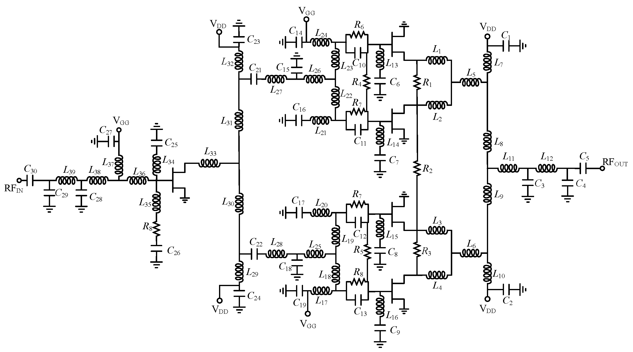
The input voltage Vgs of the FET at the gate node becomes distorted when the FET is under large-signal operation, which has a negative effect on the efficiency of the FET [11]. It is necessary to optimize the input harmonics to shape the waveform of Vgs and improve the efficiency of the FET. The input second harmonic is predominant in the distortion of Vgs, and the third and higher input harmonics can be ignored under large-signal operation [10].
Figure 3 shows the input second-harmonic source-pull results based on continuous class B mode when α = 0 and α = 1 at 10.5 GHz, when the fundamental source impedance is conjugation-matched. As shown in Figure 3a, when α = 0, the maximum efficiency in the input second-harmonic source-pull PAE contour is 70%. The second-harmonic source impedance of the maximum efficiency region is from −j × 18 Ω to −j × 4.3 Ω. Moreover, the impedance of (0.5 + j × 3.5) Ω leads to the lowest efficiency of 48%. Figure 3b shows the maximum efficiency of 70%, with impedance from −j × 6 Ω to −j × 0.15 Ω when α = 1. The impedance of (0.5 + j × 9.5) Ω leads to the worst efficiency of 54%. As shown in Figure 3, a suitable second-harmonic source impedance of the FET can improve the efficiency, and it is necessary to avoid the second-harmonic source impedance with the worst efficiency.

3. Circuit Design

The schematic of the proposed PA MMIC is shown in Figure 4. The presented high-efficiency X-band power amplifier consisting of a two-stage structure was fabricated using 0.25-μm GaN HEMT technology. The drain voltage of 28 V and quiescent current Idq of ~5% of IDmax were set as the bias point. The output stage combined four 8 × 100 μm FETs, and an 8 × 100 μm FET was utilized in the drive stage. To ensure unconditional stability of the power amplifier, an RC parallel circuit and a shunt LRC circuit were inserted at the gate of each FET in the output and drive stages, respectively. According to Figure 2, Ropt = 100 Ω for each 8 × 100 μm FET was chosen due to the tradeoff between efficiency and output power. The drain-source output capacitance CDS and parasitic inductance LD of the 8 × 100 μm FET were 0.32 pF and 18.5 pH, respectively, extracted from the PDK (Process Design Kit) provided by the foundry. Because the dissipation of the drive stage was much lower than output stage, this design focused on the output stage to improve the efficiency of the proposed PA.
Figure 5a shows the schematic of the output matching network containing the second-harmonic tuned network. Figure 5b shows the responses of second-harmonic load impedance versus L04 and C01. As shown in Figure 6, the parallel LC circuit consisted of L04 and CDS_4. CDS_4 was a constant representing the output capacitance of the FET. Because LDS_4 and L01 were much smaller the L04, the resonant frequency of the parallel LC circuit was determined by L04. As shown in Figure 5b, comparing curve A with curve B, the resonant frequency of the LC circuit varied with L04. When L04 was increased, the resonant frequency of the LC circuit decreased, and the second-harmonic frequency shifted away from the resonant frequency. This brought the second-harmonic reactance of the output matching network at 16 GHz closer to the short point.
As shown in Figure 7, the network composed of L03, C02, C03, and 50 Ω provided the resistive component in the second-harmonic frequency. The network and C01 were in parallel. As shown in Figure 5b, comparing curve A with curve C, when C01 became larger, the reactance of C01 moved closer to the short point, and the network composed of L03, C02, C03, and 50 Ω had less influence on the second-harmonic load impedance. This reduced the size of the resistive component of the second-harmonic load impedance, and the second-harmonic load impedance at 16 GHz shifted closer to the circle of Γ = 1 as C01 became larger.
Utilizing the characteristics of L04 and C01 analyzed above, the second-harmonic load impedances from 16 GHz to 21 GHz were adjusted to curve D, and other elements in Figure 5a were optimized to meet the required impedance of continuous class B mode within the fundamental frequency band, where L01 = 21 pH, L02 = 500 pH, L04 = 250 pH, and C01 = 540 f F.
As shown in Figure 8, the response of the simulated output matching network conformed to the theoretical impedance of continuous Class B mode from α = 0 to α = 0.5, as illustrated in Figure 1b.
Figure 9 shows the LC series resonant network and planes of Z1(ω), Z2(ω), and Z3(ω). In this design, an LC series resonant circuit was inserted between the FET and interstage matching network to tune the second-harmonic source impedance of the FET. Z1(ω) = A + j × B was the input impedance of the FET. Z2(ω) was the source impedance of the FET. Z3(ω) was the source impedance of the FET with an LC series resonant network. The impedance of the series LC resonant network XLC(ω) can be calculated as follows:
X L C ( ω ) = j 1 ω 2 / 4 ω 0 2 ω C ,
ω 0 = 1 2 π L C ,
where ω0 is the resonant frequency of the LC series resonant network, and Qs is the quality factor of the Z3(ω). Qs can be calculated as follows:
Q S = | I m ( Z 3 ( ω ) ) | Re ( Z 3 ( ω ) ) = | B A | + ω A 2 C + ω B 2 C A ( 1 ω 2 4 ω 0 2 ) .
Figure 10 shows the high-efficiency second-harmonic source impedance regions in the operation band. The LC series resonant network and interstage matching network were in parallel. In the second-harmonic frequency, Z2(ω) was mainly determined by XLC(ω) and Z2(ω) ≈ XLC(ω), because Z3(ω) >> XLC(ω). According to Equation (9), XLC(ω) at 21 GHz was closer to the area of inductive reactance than 16 GHz. In general design, the resonant frequency ω0 is the center frequency of the second-harmonic frequency, which removes XLC(ω) from the high-efficiency region at 21 GHz and worsens the efficiency of the power amplifier. In this design, to move XLC(ω) into the operation band into the high-efficiency region, XLC(ω) of 21 GHz was moved to the inductive side of the high-efficiency region, which was the short point in the Smith chart, and ω0 was set as 21 GHz.
According to Equation (9), XLC(ω) moved closer to the inductive region in the Smith chart as C became larger. Therefore, XLC(ω) at 16 GHz was moved into the high-efficiency region when C was increased. According to Equation (11), an increase in C would result in Qs becoming larger, leading to the deterioration of the bandwidth. In this design, XLC(ω) at 16 GHz was moved to the boundary of the high-efficiency region by adjusting the value of C. Then, the lowest Qs was achieved when the high-efficiency performance of the power amplifier was assured. The reactance in the boundary of the high-efficiency region was −j × 28 Ω in Figure 10. According to Equations (9) and (10), L = 0.16 nH and C = 0.35 pF were obtained.
Figure 11 shows the stability of the proposed PA under small-signal and large-signal conditions. As shown in Figure 11a, the stability factors of the FETs in both stages were larger than the unit, revealing that the PA is stable under small-signal operation. The large-signal stability result of the proposed PA from 8 GHz to 10.5 GHz was determined using STAN software according to the pole-zero identification method [15], as shown in Figure 11b. As shown in Figure 11b, there were no unstable poles in the right half of the plane, which shows that the proposed PA is stable under large-signal operation.

4. Measurement Results

The photograph of the proposed PA MMIC is shown in Figure 12. The chip dimension was 3.2 × 2.4 mm2. The proposed PA was measured under the pulse condition with a 100-μs pulse width and a duty cycle of 10%. The simulated and measured performances are summarized in Figure 13. As shown in Figure 13a, the measured saturated output power was within 40.8–42.2 dBm and 19.8–21.2 dB gain was achieved from 8 GHz to 10.5 GHz. The measured PAE at the saturated output power was 51.7–59% from 8 GHz to 10.5 GHz. As for the performance with a small signal, shown in Figure 13b, S21 ranged from 23.6 dB to 25.6 dB and S11 was lower than −10 dB from 8 GHz to 10.5 GHz. The difference between the measured |S21| and simulated |S21| was due to the increase in threshold voltage in the PA MMIC tapering out. Table 1 shows a comparison with recent reported state-of-the-art X-band PAs, which reveals that the proposed PA performs competitively in terms of efficiency and operation bandwidth. The presented PA in Reference [16] had an excellent performance in terms of PAE because it utilized an output second- and third-harmonic tuned method, which sacrificed performance in terms of operation bandwidth. Compared with the traditional harmonic controlled PA, the proposed PA has a wider operation bandwidth at the same level of efficiency.

5. Conclusions

This work presented an X-band high-efficiency power amplifier MMIC implemented in 0.25-μm GaN technology. The high-efficiency operation bandwidth of the proposed PA was extended with continuous class B mode utilizing an optimized output second-harmonic tuned network. Meanwhile, the efficiency of the proposed PA was improved through optimum second-harmonic source impedance and Ropt derived using the Pedro load-line method. The optimum second-harmonic impedance was tuned into the high-efficiency region utilizing an LC series circuit in the operation band. The quality factor of the fundamental source impedances was taken into consideration to determine the values of L and C in the LC series circuit. The method mentioned above was well verified in the presented PA, and excellent performance with a bandwidth of 27% and an efficiency of 59% was achieved.

Author Contributions

Methodology, C.J.; software, Y.G.; validation, W.C.; data curation, J.H.; writing—original draft preparation, C.J.; writing—review and editing, Z.W.; supervision, F.Y.; project administration, J.H.; funding acquisition, J.M.

Funding

This work was supported in part by the National Natural Science Foundation of China under Grant 61604128 and the Fundamental Research Funds for the Central Universities under Grant 2017QN81002.

Acknowledgments

The authors would like to thank the Institute of Aerospace Electronics Engineering of Zhejiang University for providing the research platform and technical support.

Conflicts of Interest

The authors declare no conflicts of interest.

References

  1. Tasker, P.J.; Carrubba, V.; Wright, P.; Lees, J.; Benedikt, J.; Cripps, S.; Wideband, P.A. Design: The “Continuous” Mode of Operation. In Proceedings of the IEEE Compound Semiconductor Integrated Circuit Symposium (CSICS), La Jolla, CA, USA, 14–17 October 2012; pp. 1–4. [Google Scholar]
  2. Cipriani, E.; Colantonio, P.; Giannini, F. Class F-C X-band MMIC GaN power amplifier: An extension of waveform engineering approach. In Proceedings of the Integrated Nonlinear Microwave and Millimeter-wave Circuits Workshop Digest, Graz, Australia, 20–21 April 2017; pp. 1–4. [Google Scholar]
  3. Gao, S.; Butterworth, P.; Sambell, A.; Sanabria, C.; Xu, H.; Heikman, S.; Mishra, U.; York, R.A. Microwave Class-F and Inverse Class-F Power Amplifiers Designs using GaN Technology and GaAs pHEMT. In Proceedings of the European Microwave Conference Digest, Manchester, UK, 10–13 September 2006; pp. 439–496. [Google Scholar]
  4. Forouzanfar, M.; Feghhi, R.; Baseri, J.; Joodaki, M. High efficiency 8.8–9.6 GHz class J power amplifier. In Proceedings of the 16th Mediterranean Microwave Symposium, Abu Dhabi, UAE, 14–16 November 2016; pp. 1–4. [Google Scholar]
  5. Liu, B.; Mao, M.; Boon, C.C.; Choi, P.; Khanna, D.; Fitzgerald, E.A. A Fully Integrated Class-J GaN MMIC Power Amplifier for 5-GHz WLAN 802.11ax Application. IEEE Microw. Wirel. Compon. Lett. 2018, 28, 434–436. [Google Scholar] [CrossRef]
  6. Cripps, S.; Tasker, P.J.; Clarke, A.L.; Lees, J.; Benedikt, J. On the Continuity of High Efficiency Modes in Linear RF Power Amplifiers. IEEE Microw. Wirel. Compon. Lett. 2009, 19, 665–667. [Google Scholar] [CrossRef]
  7. Powell, J.R.; Uren, M.J.; Martin, T.; McLachlan, A.; Tasker, P.; Woodington, S.; Bell, J.; Saini, R.; Benedikt, J.; Cripps, S.C. GaAs X-band high efficiency(>65%) Broadband (>30%) amplifier MMIC based on the Class B to Class J continuum. In Proceedings of the IEEE MTT-S International Microwave Symposium, Baltimore, MD, USA, 5–10 June 2011; pp. 1–4. [Google Scholar]
  8. Cripps, S.C. RF Power Amplifiers for Wireless Communications, 2nd ed.; Artech House: Norwood, MA, USA, 2006; pp. 21–27. [Google Scholar]
  9. Pedro, J.C.; Nunes, L.C.; Cabral, P.M. A Simple Method to Estimate the Output Power and Efficiency Load-Pull Contours of Class-B Power Amplifiers. IEEE Trans. Microw. Theory Tech. 2015, 63, 1239–1249. [Google Scholar] [CrossRef]
  10. Sharma, T.; Srinidhi, E.R.; Darraji, R.; Holmes, D.G.; Staudinger, J.; Jones, J.K.; Ghannouchi, F.M. High-Efficiency Input and Output Harmonically Engineered Power Amplifiers. IEEE Trans. Microw. Theory Tech. 2017, 66, 1002–1014. [Google Scholar] [CrossRef]
  11. Colantonio, P.; Giannini, F.; Limiti, E. High Efficiency RF and Microwave Solid State Power Amplfiers; John Wiley & Sons Ltd.: West Sussex, UK, 2009; p. 303. [Google Scholar]
  12. Canning, T.; Tasker, P.; Cripps, S. Waveform Evidence of Gate Harmonic Short Circuit Benefits for High Efficiency X-Band Power Amplifiers. IEEE Trans. Microw. Theory Tech. 2013, 23, 439–441. [Google Scholar] [CrossRef]
  13. Colantonio, P.; Giannini, F.; Leuzzi, G.; Limiti, E. High efficiency low-voltage power amplifier design by second-harmonic manipulation. Int. J. RF Microw. Comput. Aided Eng. 2000, 10, 19–32. [Google Scholar] [CrossRef]
  14. Colantonio, P.; Giannini, F.; Leuzzi, G.; Limiti, E. Multiharmonic manipulation for highly efficient microwave power amplifiers. Int. J. RF Microw. Comput. Aided Eng. 2001, 11, 366–384. [Google Scholar] [CrossRef]
  15. Anakabe, A.; Ayllón, N.; Collantes, J.M.; Mallet, A.; Soubercaze-Pun, G.; Narendra, K. Automatic Pole-Zero Identification Multivariable Large-Signal Stability Analysis of RF and Microwave Citcuits. In Proceedings of the 40th European Microwave Conference, Paris, France, 28–30 September 2010; pp. 477–480. [Google Scholar]
  16. Sardin, D.; Reveyrand, T.; Popovi´c, Z. X-band 10 W MMIC High-Gain Power Amplifier with up to 60% PAE. In Proceedings of the 2014 9th European Microwave Integrated Circuit Conference, Rome, Italy, 6–7 October 2014; pp. 393–396. [Google Scholar]
  17. Resca, D.; Raffo, A.; Falco, D.S.; Scappaviva, F.; Vadalà, V.; Vannini, G. X-Band GaN Power Amplifier for Future Generation SAR Systems. IEEE Microw. Wirel. Compon. Lett. 2014, 24, 266–268. [Google Scholar] [CrossRef]
  18. Bae, K.T.; Lee, L.K.; Kang, B.; Sim, S.; Jeon, L.; Kim, D.W. X-Band GaN Power Amplifier MMIC with a Third Harmoninc-Tuned Circuit. Electronics 2017, 6, 103. [Google Scholar] [CrossRef]
  19. Couturier, A.M.; Poitrenaud, N.; Serru, V.; Dionisio, R.; Fontecavc, J.J.; Camiade, M. 50% High Efficiency X-Band GaN MMIC Amplifier for Space Applications. In Proceedings of the 48th European Microwave Conference, Madrid, Spain, 23–27 September 2018; pp. 352–355. [Google Scholar]
  20. Piotrowicz, S.; Ouarch, Z.; Chartier, E.; Aubry, R.; Callet, G.; Floriot, D.; Jacquet, J.-C.; Jardel, O.; Morvan, E.; Reveyrand, T.; et al. 43W, 52% PAE X-Band AlGaN/GaN HEMTs MMIC Amplifiers. In Proceedings of the 2010 IEEE MTT-S International Microwave Symposium Digest, Anaheim, CA, USA, 23–28 May 2010; pp. 505–508. [Google Scholar]
Figure 1. (a) The normalized voltage waveforms of continuous class B power amplifiers (PAs) from α = −- to α = 1. (b) The desired fundamental and harmonic load impedances at the current source node of the field-effect transistor (FET) in continuous class B mode.
Electronics 08 01312 g001
Figure 2. (a) Drain efficiency and (b) output power of the 8 × 100 μm FET calculated using the Pedro load-line method.
Electronics 08 01312 g002
Figure 3. Input second-harmonic source-pull simulation results of 8 × 100 μm FET with continuous class B mode at 10.5 GHz: (a) α = 0; (b) α = 1.
Electronics 08 01312 g003
Figure 4. The schematic of the presented high-efficiency power amplifier.
Electronics 08 01312 g004
Figure 5. (a) The schematic of the output matching network; (b) the responses of second-harmonic load impedance versus L04 and C01
Electronics 08 01312 g005
Figure 6. The simplified output second-harmonic tuned network when L04 is analyzed.
Electronics 08 01312 g006
Figure 7. The simplified output matching network when C01 is analyzed.
Electronics 08 01312 g007
Figure 8. The simulated response of the output matching network from 8 GHz to 21 GHz.
Electronics 08 01312 g008
Figure 9. The LC series resonant network and the planes of Z1(ω), Z2(ω), and Z3(ω).
Electronics 08 01312 g009
Figure 10. High-efficiency second-harmonic source impedance regions in the operation band, and the response of the second harmonic source impedance of the FET.
Electronics 08 01312 g010
Figure 11. (a) Small-signal stability factor of the output stage and driver stage in the proposed PA; (b) large-signal stability results for the proposed PA using the pole-zero identification method.
Electronics 08 01312 g011
Figure 12. Photograph of the proposed X-band power amplifier.
Electronics 08 01312 g012
Figure 13. (a) Simulated and measured Pout, PAE, and gain versus frequency from 7.5 GHz to 11.5 GHz; (b) simulated and measured S-parameter versus frequency from 7.5 GHz to 11.5 GHz; (c) simulated and measured gain versus input power at 10 GHz.
Electronics 08 01312 g013
Table 1. Comparison with recent reported state-of-the-art X-band power amplifier (PA) MMICs.
ReferenceTechnologyOperation ModeFrequency
(GHz)
Pout
(dBm)
PAE
(%)
Gp
(dB)
Pulse/Duty
(μs, %)
[16]0.15 μm GaNClass AB,
output 2nd and 3rd harmonic tuned
10–10.54045–6119Continuous Wave
[17]0.25 μm GaNClass AB8.8–10.440–4138–4417–1850, 15
[18]0.25 μm GaNClass AB,
3rd harmonic tuned
8.5–10.543.2–44.735–3716–19.1100, 10
[19]0.25 μm GaNClass AB,
input and output 2nd harmonic tuned
7.8–8.843.550–5218.5Continuous Wave
[20]0.25 μm GaN Class AB8.5–1143–46.533–5213–16.520, 10
This work0.25 μm GaNContinuous class B,
input 2nd harmonic tuned
8–10.540.8–42.251.7–5919.8–21.2100, 10

