Article

Switching Loss Balancing Technique for Modular Multilevel Converters Operated by Model Predictive Control Method

School of Electrical and Electronic Engineering, Chung-ang University, Seoul 06974, Korea
*
Author to whom correspondence should be addressed.
Electronics 2019, 8(10), 1175; https://doi.org/10.3390/electronics8101175
Submission received: 18 September 2019 / Revised: 10 October 2019 / Accepted: 15 October 2019 / Published: 16 October 2019
(This article belongs to the Section Power Electronics)

Abstract

:
The sorting algorithm is the most widely accepted capacitor voltage balancing strategy for a modular multilevel converter. This strategy offers to keep the balance among submodule capacitor voltages under all of the modular multilevel converter working conditions. However, this method generates unnecessary switching transitions in submodules, which results in high switching frequency and switching loss, and uneven distribution of switching transitions and switching loss among submodules (SMs). In this paper, a simplified switching loss balancing control strategy was proposed in order to handle these issues. The proposed approach adjusted the submodule selection process of the sorting algorithm by taking into consideration the number of switching transitions in addition to the capacitor voltages. Even distribution of switching transitions and switching loss was achieved, and the average switching loss was reduced at the cost of slightly increasing the capacitor voltage fluctuations. The effectiveness of the proposed approach was verified through both simulation and experimental results.

1. Introduction

Modular multilevel converter (MMC) has received a great deal of concern due to numerous advantages [1,2,3] such as a highly modular structure, easy scalability, and superior harmonic performance. Since it was first introduced in 2003 [4] by Lesnicar and Marquardt, MMC has become the most potential topology for medium- to high-power applications, specifically for the high-voltage direct current (HVDC) application.
In spite of the benefits of MMC, the control of this converter is quite challenging due to multiple control objectives. In order to guarantee proper operation of MMC, proper magnitude and frequency of output current, suppression of circulating current, and balance of submodule (SM) capacitor voltages must be satisfied. Various control methods have been studied extensively to address these requirements. Earlier, classical control method used proportional-integral (PI) [5] and proportional-resonant (PR) [6] controllers, combining a pulse-width modulator to control each objective. A typical control scheme, which was presented in [5,7], uses PI controllers and applies a pulse-width modulation (PWM) scheme to MMC with averaging and balancing control. Aside from this, different multicarrier PWM techniques have been reported [8,9,10,11] in evaluating their performance to MMC. The performance of classical control method is mostly influenced by the design and tuning of the PI controller’s parameters, as well as the selected PWM type.
In recent years, model predictive control (MPC) [12,13,14] has been considerably involved in the control of MMC due to its capability of handling the drawbacks of the classical control method. Owing to distinctive advantages such as the capability of controlling multiple objectives simultaneously with a single cost function, superior dynamic performance, and inclusion of system’s nonlinearity, MPC has been extensively studied in recent years. The basic idea of MPC is to evaluate all possible switching states of a converter to obtain the optimal one through calculation of a predefined cost function. This MPC scheme refers to direct MPC [15,16], in which 22N (N is the number of SMs in one arm) possible switching states are evaluated in every sampling instant for MMC. The best switching state is selected from the minimum value for the cost function, which results in optimal value of the output current, circulating current, and SM capacitor voltages errors. In spite of straightforward implementation, the direct MPC suffers from computational burden due to the number of possible switching states increasing exponentially as the number of SMs increase. In order to handle this drawback, a standard method, which is widely applied to reduce the computational burden, is used to classify control objectives at different stages [17,18,19,20]. As in [17], this approach uses three independent cost functions corresponding to output current, circulating current, and capacitor voltages balancing to obtain optimal switching state. However, this method does not provide the flexibility of interaction among control objectives. A more popular scheme, which is referred as indirect MPC, is investigated in [20]. The indirect MPC decouples the capacitor voltage balancing task from the cost function using a voltage-sorting algorithm. In this case, the MPC is responsible for evaluating the optimal number of inserted SMs in the upper and lower arms, whereas the sorting algorithm could decide which SM should be inserted or bypassed in order to retain the balance of capacitor voltages among SMs.
Different from the conventional direct MPC, the voltage-sorting algorithm is implemented in the indirect MPC to carry out the SM capacitor voltage balancing task. This sorting method is the most widely accepted SM capacitor voltage balancing strategy [21,22], achieved by using the sorted capacitor voltages among SMs and direction of the arm current to determine which SM should be inserted or bypassed. In spite of the guarantee of SM capacitor voltage balancing under various MMC operating conditions, the sorting algorithm generates unnecessary switching transitions among SMs due to it needing to be implemented in every control period. This results in a case in which the number of inserted SMs within two adjacent control periods are precisely similar, wherein the inserted or bypassed actions of SM may occur. Thus, due to unnecessary switching transitions, the sorting algorithm leads to increased switching frequency and relatively high switching losses. Additionally, as for long-time MMC operation, it might result in a tremendous difference of switching transition number, switching frequency, and switching losses among SMs. Several methods, which aim at reducing the switching frequency, are proposed in [23,24,25]. In [23], a limited number of SMs are sorted within each control period to prevent unnecessary switching transitions. It means that if additional SMs in each arm need to be inserted (bypassed), the conventional sorting algorithm will only be applied to bypassed (inserted) SMs. Although this method significantly reduces the switching frequency, it may result in a higher capacitor voltage fluctuation due to the SM staying inserted or bypassed for a long time. Additionally, the previously reduced switching frequency methods do not balance the switching transitions and switching losses among SMs.
In this paper, a simplified switching loss balancing control strategy was proposed. The proposed approach allowed balancing the switching losses, reducing average switching transition and switching loss among SMs, and eliminating unnecessary switching transitions in conventional sorting algorithm. This simplified switching loss balancing adjusted the SM selection process of the sorting algorithm by taking into consideration the number of switching transitions in addition to the capacitor voltages. Moreover, the desired tolerance band of the capacitor voltage was set to avoid tremendous capacitor voltage fluctuation. Simulation results were provided to verify the effectiveness of the proposed approach in terms of balancing both the capacitor voltages and the switching loss. Additionally, a single-phase seven-level MMC laboratory prototype was also used to implement and validate the proposed approach.
This paper is organized as follows: Section 2 presents an introduction about the underlying structure and operation of MPC and the basic MPC schemes. Section 3 explains the conventional sorting algorithm and the proposed approach in detail as for balancing both capacitor voltages and switching loss. Simulation and experimental results are discussed in Section 4, whereas Section 5 draws the conclusion.

2. Structure and Model Predictive Control of MMC

2.1. Standard Structure and Model of Single-Phase MMC

Figure 1 depicts a generalized configuration of a single-phase MMC. A converter phase consists of two arms, namely the upper arm and lower arm. The two identical arms were represented by a subscript “u” and “l” for upper arm and lower arm, respectively. In this, each arm was composed of N SMs, which connected in series with an inductor La that was in charge of limiting arm currents. As for SM, the MMC could be structured by various type of SMs, corresponding to the application, operating voltage, and power [26]. In this investigation, owing to its simplicity and low power-loss characteristics, a basic half-bridge SM topology was used. The half-bridge SM can only produce zero and positive output voltage, depending on the state of its two complementary switches Sj and Sj (j = 1 − N).
In Figure 1, the mathematical model of MMC can be generated by applying Kirchhoff’s law. Output current io and circulating current icirc equations can be derived by using Kirchhoff’s current law as follows:
i o = i u i l ,
i c i r c =   1 2 ( i u +   i l ) ,
where iu and il are the upper and lower currents, respectively. Similarly, the voltage relationship of the MMC according to Kirchhoff’s voltage law can be expressed as
V d c 2   v u   L a d i u ( k ) d t R i o L d i o ( k ) d t = 0 ,
V d c 2 +   v l +   L a d i u ( k ) d t R i o L d i o ( k ) d t = 0 ,
where Vdc is dc-link voltage, whereas vu and vl represent the upper and lower arm voltages, respectively. L and R represent load inductance and resistance, respectively.
Adding (3) and (4), and subtracting (3) from (4), mathematical dynamics of the output and circulating currents are deduced as
d i o ( k ) d t =   ( 1 2 L +   L a ) [ v l ( k )   v u ( k ) 2 R i o ( k ) ] ,
d i c i r c ( k ) d t =   ( 1 2 L a ) [ V d c   v u ( k )   v l ( k ) ] .
From (5) and (6), the output current only corresponded to the difference of the upper and lower arm voltages, whereas the circulating current related to the sum of the upper and lower arm voltages.

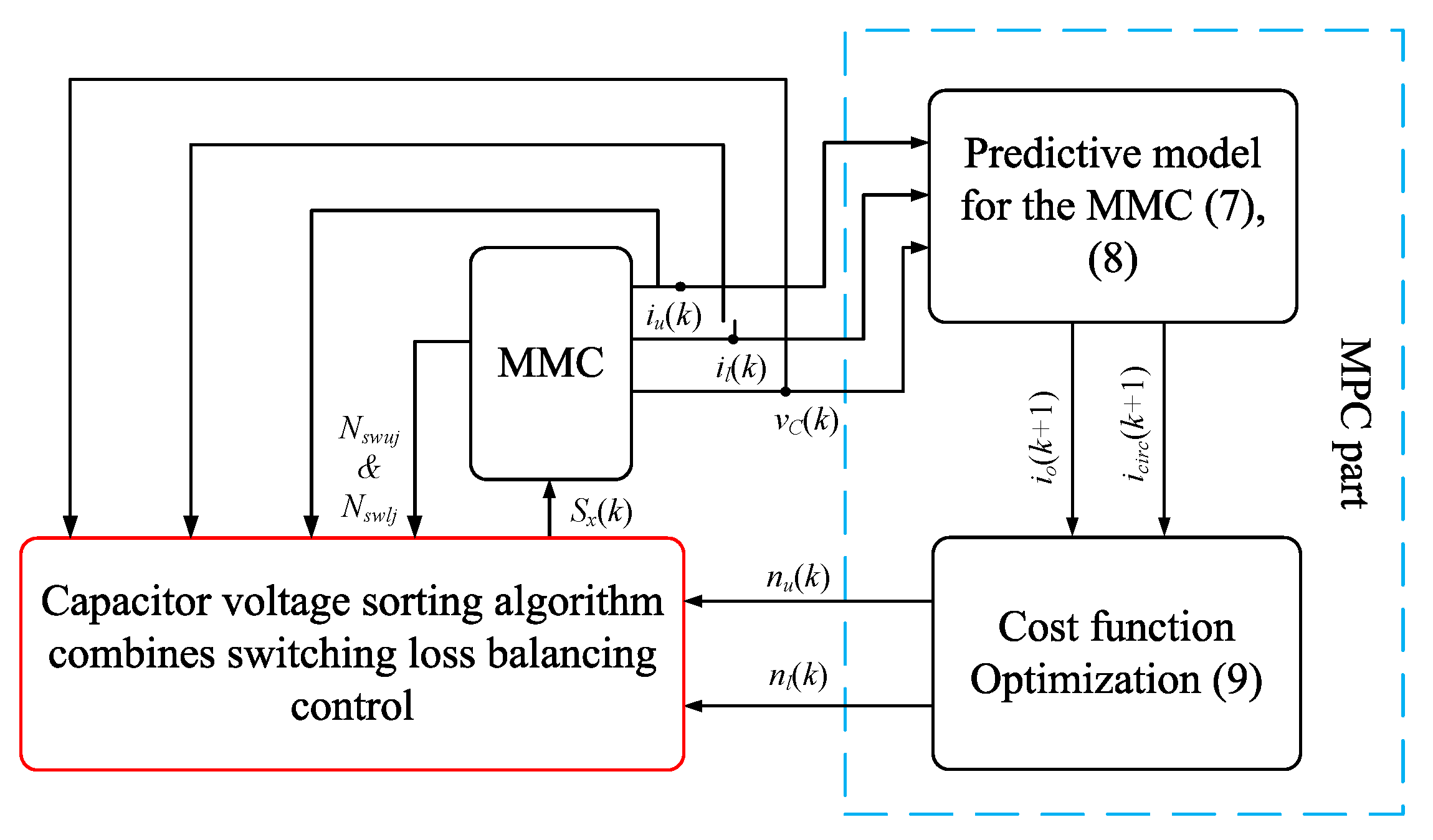
2.2. Model Predictive Control for MMC

Due to the challenging control of MMC, which involves various control objectives such as the proper magnitude and frequency of output current, circulating current suppression, and capacitor voltage balancing, the MMC requires a proper and robust control scheme to achieve these control objectives. In recent years, the MPC is known as an advantageous approach to control the MMC, owing to numerous advantages such as capability in controlling multiple objectives simultaneously with a single cost function and superior dynamic performance [27].
Although the direct MPC is straightforward to implement, it suffers from a substantial computational burden due to 22N possible switching states when evaluating every sampling instant. The indirect MPC proposed in [20] can help to reduce the computational burden. It can be observed from Figure 2 that the indirect MPC was different from the direct MPC in terms of decoupled SM capacitor voltage balancing. In this case, the capacitor voltage balancing term was not included in the cost function, whereas the MPC scheme evaluated the number of inserted SMs nu and nl in the upper and lower arms, respectively. Subsequently, a voltage sorting algorithm [21] can determine which SM should be inserted or bypassed in order to generate switching signal, as well as keeping capacitor voltages balancing. In this paper, the indirect MPC that was implemented in simulation and experimental studies is reviewed in detail for the single-phase MMC in Figure 1.
Due to the MPC operating in the discrete-time domain, it required the discrete-time domain mathematical model of control objectives. Applying the Euler approximation [12] to (5) and (6), the discrete-time model of the output and circulating current can be deduced as follows:
i o ( k + 1 ) =   ( T s p 2 L + L a ) ( v l ( k )   v u ( k ) ) + ( 1 2 R T s p 2 L + L a ) i o ( k ) ,
i c i r ( k + 1 ) =   ( T s p 2 L a ) [ V d c   v u ( k )   v l ( k ) ] + i c i r c ( k ) .
A cost function g was designed to determine the optimal number of inserted SMs every sampling instant on the basis of the difference between the predicted output and circulating currents and the reference values ( i o ( k + 1 ) and i c i r c ( k + 1 ) ), respectively. The cost function g can be expressed as
g =   w 1 | i o ( k + 1 ) i o ( k + 1 ) | + w 2 | i c i r c ( k + 1 ) i c i r c ( k + 1 ) | ,
where w1 and w2 are the corresponding weighting factors. It should be noted that the weighting factors used in the cost function had significant effects on the quality of control objectives. The selection of these weighting factors was based on [28], in order to guarantee the optimal quality of control objectives.

3. Conventional Sorting Algorithm and Proposed Switching Loss Balancing Control Strategy

3.1. Conventional Sorting Algorithm

The conventional sorting algorithm has received a great deal of attention in implementing the capacitor voltage balancing task. The basic idea of the sorting algorithm is based on the effect of arm currents on SM capacitor voltage. When the upper (lower) arm current is positive, if an SM is inserted, the corresponding SM capacitor voltage will increase because the SM capacitor is charged. On the other hand, if the upper (lower) arm current is negative, the SM capacitor will be discharged, which results in a decrease of corresponding capacitor voltage. As for bypassed SM, neither positive arm currents nor negative arm currents charge or discharge the corresponding SM capacitor. In this case, the capacitor voltage is unchanged.
In order to keep capacitor voltages balanced, the SM capacitor voltages from both arms are measured and sorted, whereas the upper and lower arm currents are considered to decide which SM should be inserted or bypassed. If the upper (lower) arm current is positive, nu (nl) SMs with the lowest voltages are determined and inserted, whereas the others are bypassed. Consequently, the corresponding SM capacitors are charged, and their voltages increase as well. If the upper (lower) arm current is negative, nu (nl) SMs with the highest voltages are inserted to discharge, and the others are bypassed. The corresponding capacitor voltages are decreased to retain the capacitor voltage balancing. A block diagram of the conventional sorting algorithm is presented in Figure 3.
Because the sorting algorithm inserts or bypasses the SMs according to their corresponding capacitor voltages, the conventional sorting algorithm can produce unnecessary switching transitions among the SMs, which results in the high switching frequency. Moreover, as the characteristic of each SM is different, this leads to uneven switching transitions and switching loss distribution among SMs under the conventional sorting algorithm.

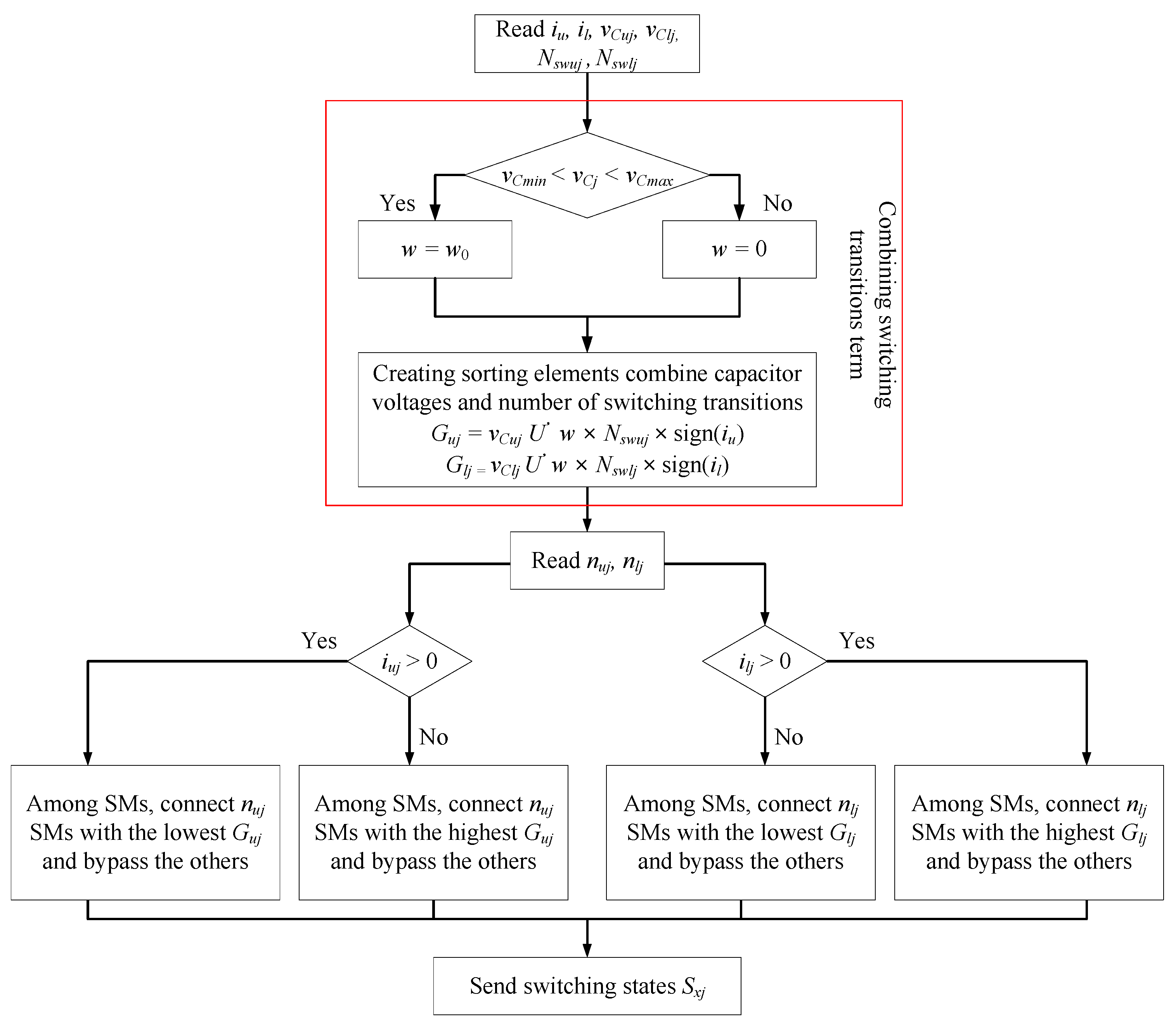
3.2. Proposed Switching Loss Balancing Control
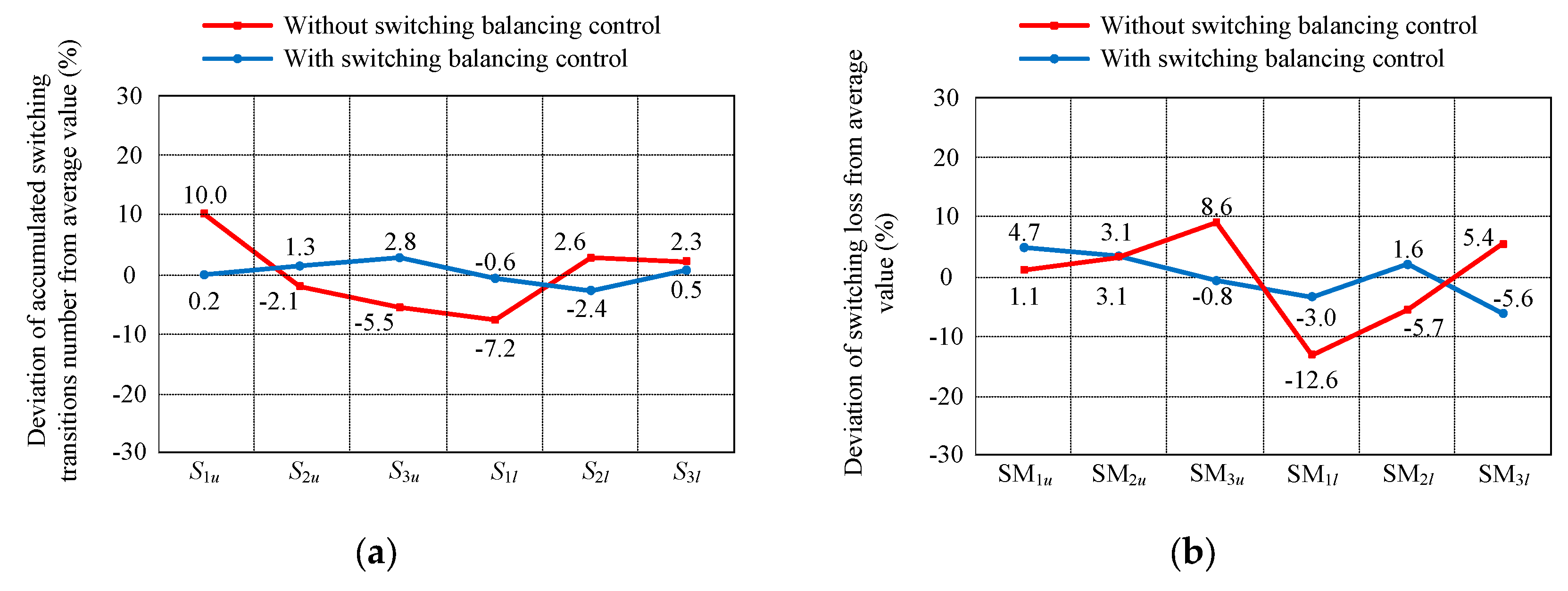
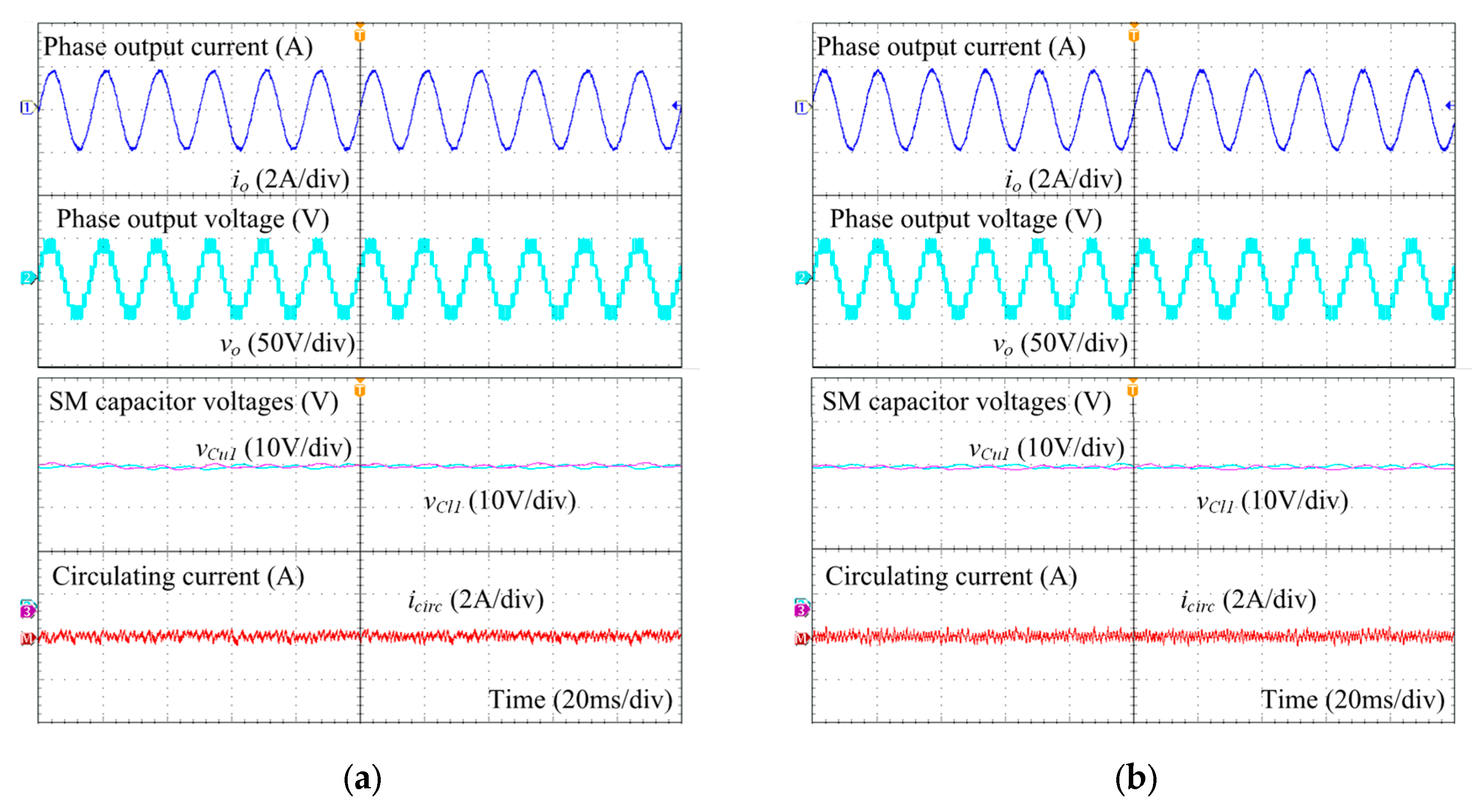
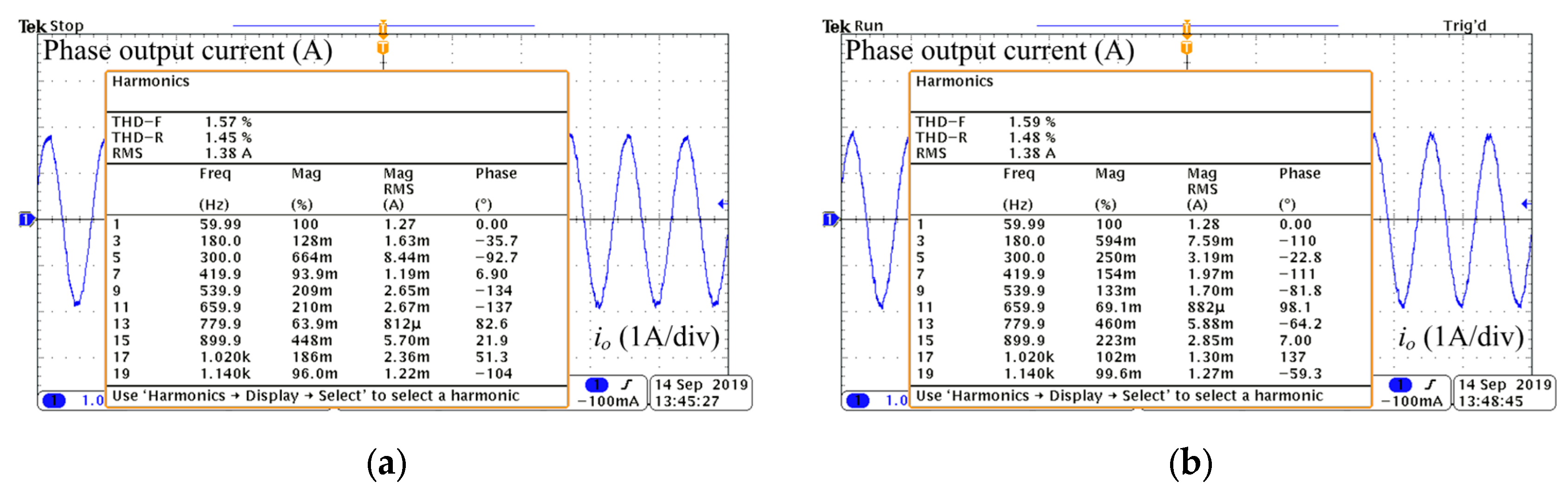
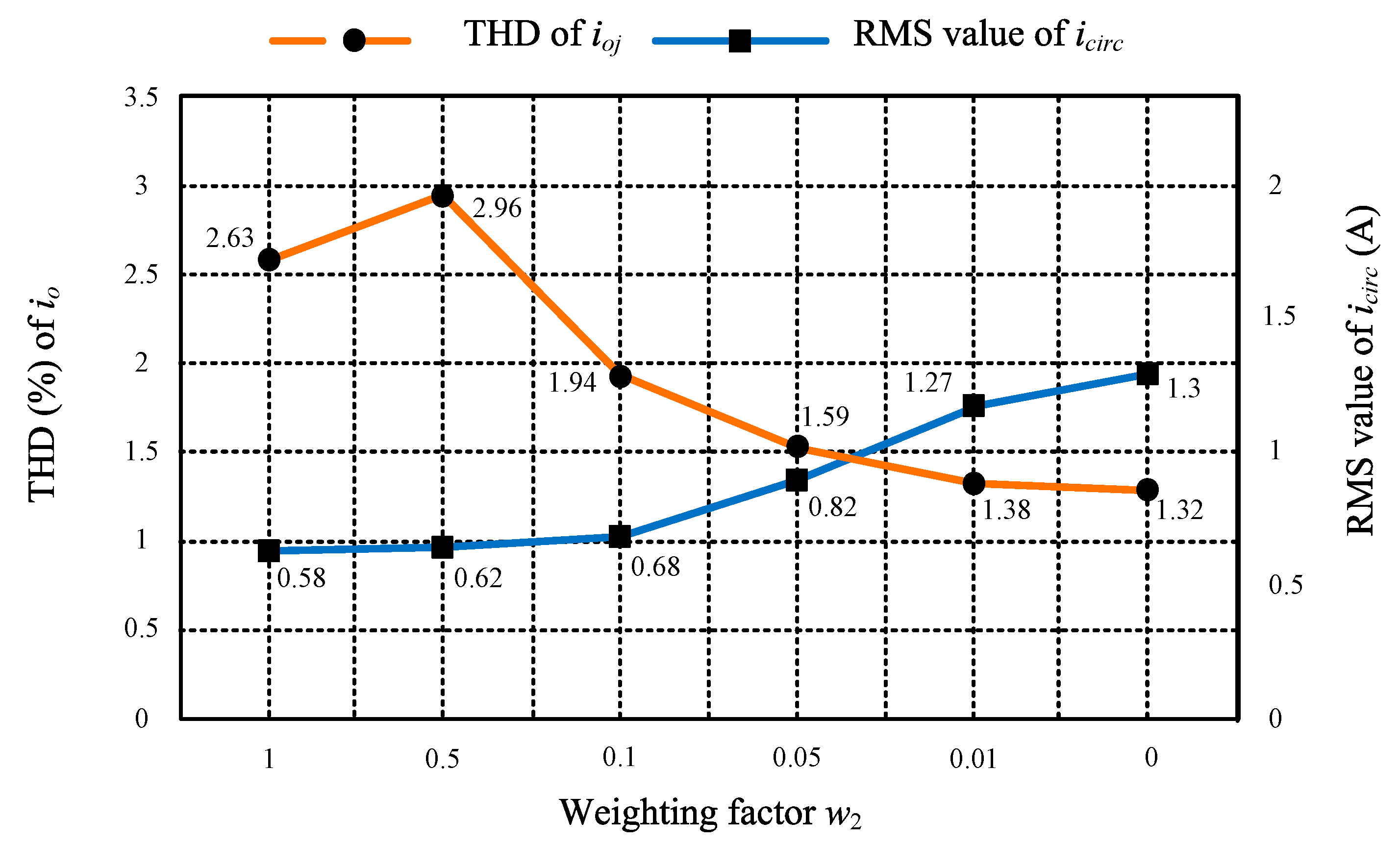
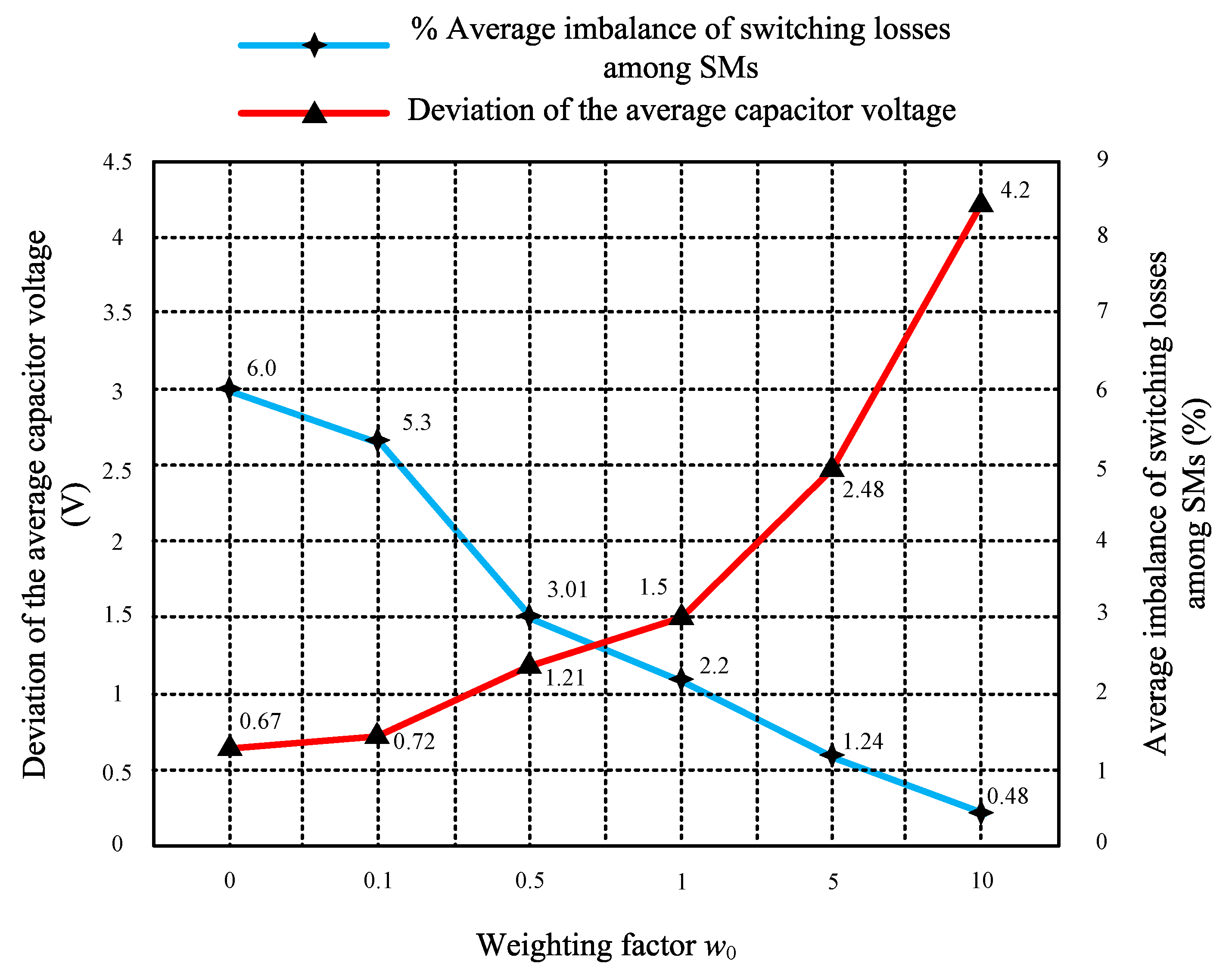
In order to solve the issues presented above, the simplified switching loss balancing control was proposed by combining the conventional sorting algorithm and switching loss balancing control term. Here, the number of the switching transitions of the switch Sj is used for balancing, as the switches Sj and Sj are complementary. A flow chart of the proposed approach is shown in Figure 4.
The SM capacitor voltages and arm currents are first measured, and the number of switching transitions is counted. Subsequently, a cost function Gj corresponding to each SM is calculated as follows:
G u j =   v C u j w × N s w u j × sign ( i u ) ,
G l j =   v C l j w × N s w l j × sign ( i l ) ,
where w is the weighting factor, Nswuj and Nswlj represent the number of switching transitions of each upper arm and lower arm SMs, respectively. The calculated cost functions Guj and Glj play the same role as SM capacitor voltages in the conventional sorting algorithm. This means that when the calculation of Guj and Glj for each SM is completed, they are sorted and the selection of SM is operated as in the conventional sorting algorithm. The number of switching transitions terms allow for the adjusting of the SM selection process to guarantee not only the capacitor voltage balancing but also switching loss balancing.
Due to the fact that the SM selection process is modified by adopting this method, it is possible that SMs are kept in an inserted or bypassed condition for a long time, which results in excessive capacitor voltage deviation. This exerts a negative impact on capacitor voltages balancing. In order to handle this problem, the desired tolerance band is set with an acceptable peak-to-peak value of the SM capacitor voltage at 2% of the nominal value Vdc/N. This can be expressed as follows:
v C m i n v C j v C m a x ,
where v C m i n = 0.98 V d c N , and v C m a x = 1.02 V d c N . If the SM capacitor voltage exceeds its voltage band, the proposed switching loss balancing control is disabled by assigning the weighting factor w as zero (w = 0). On the other hand, if the SM capacitor voltage is within its voltage band, the proposed approach is enabled and the weighting factor w = w0 is assigned.
The selection of the weighting factor is carefully designed to balance both capacitor voltages and switching losses by using the method in [28]. Additionally, the direction of arm currents sign(iu) and sign(il) are multiplied with the number of switching transitions terms, as the cost functions Guj and Glj are sorted in the opposite order when the arm current direction changes. With the use of the proposed approach, the balancing of both capacitor voltages and switching losses can be achieved.
The control structure of the MMC, including the proposed approach, is shown in Figure 5. The optimal number of inserted SMs in upper and lower arms (nu(k) and nl(k)) are obtained according to the cost function described in (9). Subsequently, the capacitor voltage sorting algorithm combines switching loss balancing control, generating the gate signals of the SMs.

4. Results

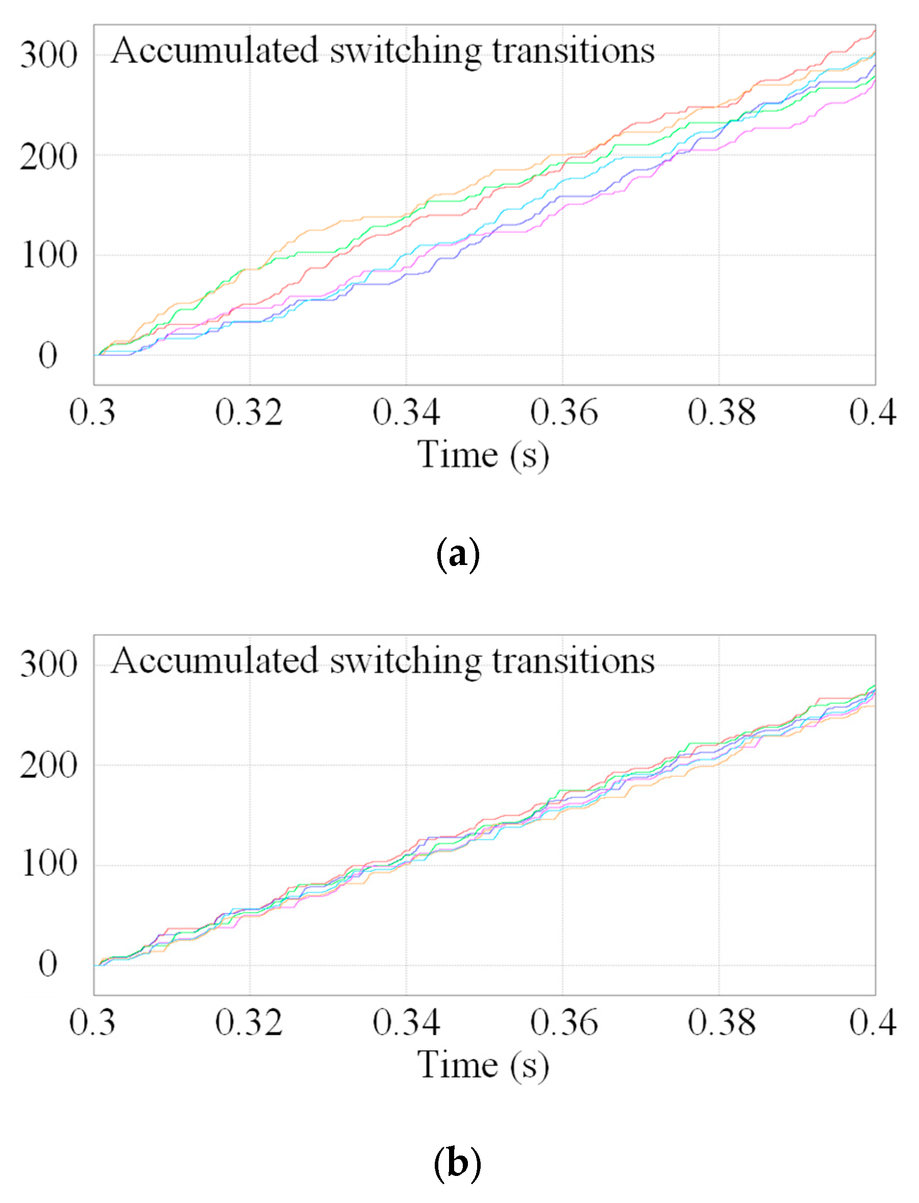
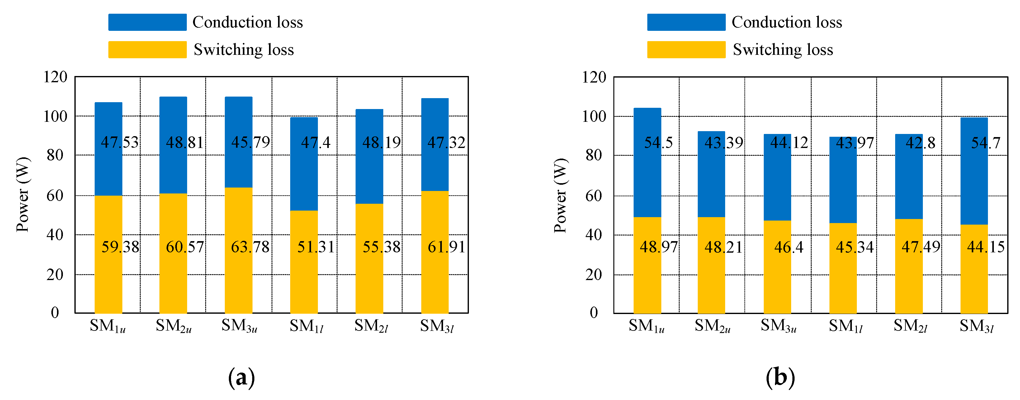
4.1. Simulation Study

In order to verify the effectiveness of the proposed approach, the simulation of a single-phase MMC with N = 3 was carried out using PSIM software, the system’s parameters for which are given in Table 1.
The weighting factors, which are listed in Table 2, were used in both the simulation and experiment. The weighting factors selection procedure, based on [28], is shown in Appendix A.
The phase output current, phase output voltage, SM capacitor voltages, and circulating current generated by the conventional indirect MPC without and with using switching loss balancing control during steady-state operation are shown in Figure 6a,b, respectively.
The results of the steady-state operation depicted in Figure 6b showed excellent steady-state performance. The output current in Figure 6b had a correct sinusoidal form with total harmonic distortion THD = 1.27%, which slightly increased compared to the output current in Figure 6a with THD = 1.24%. The phase output voltage level from both of two figures contained sufficiently seven-levels that varied in the range −Vdc/2 to Vdc/2, whereas the circulating currents were well-suppressed. These results can be noticed from Figure 6b, wherein the deviation of capacitor voltages was higher than the results from Figure 6a. This was a trade-off when the switching loss balancing control strategy was adopted. From the magnification of SM capacitor voltages in Figure 7a, it was shown that the deviation of capacitor voltages from nominal value Vdc/N under which without applying switching loss balancing control was approximately 0.7%. This deviation from Figure 7b, when applying switching loss balancing control strategy, was about 1.2%, which was still acceptable with the desired tolerance band proposed in Section 3. This slight increase in terms of capacitor voltage deviation had a minor effect on quality of MMC performance thanks to the optimal designed weighting factor and tolerance band. In Figure 7c, the SM capacitor voltage waveforms are presented under the application of the proposed method but without optimal weighting factor w0 and tolerance band. It was apparent that without using optimal weighting factor and tolerance band, the balance of capacitor voltages among SMs was not guaranteed. The difference of MMC performance in terms of phase output current, phase output voltage, and circulating current between with and without applying the proposed method was not noticeable. This verified that the proposed method does not deteriorate the MMC performance.
Figure 8 shows the number of accumulated switching transitions within the time interval of 0.1 s of all SMs without applying switching loss balancing control and with applying switching loss balancing control. As observed in Figure 8a, the number of accumulated switching transitions among SMs was mainly divergent. This resulted in different switching frequencies, as well as switching loss distribution among SMs. It can be seen that the maximum switching transition number difference was 51 switching transitions. However, it significantly decreased to 13 switching transitions for SMs when applying the switching loss balancing control strategy, as in Figure 8b. Furthermore, the average number of switching transitions when applying the proposed switching loss balancing control strategy was smaller than without applying the switching loss balancing control.
The switching losses and conduction loss evaluation were investigated on the basis of the method used in [22]. The parameters of the insulated-gate bipolar transistor (IGBT) modules were derived from the datasheet of the BSM 50GB 60DLC from Infineon [29]. The junction temperature Tj was considered to be 125 °C for the loss performance calculation. The comparison between power losses of each SM is shown in Figure 9a,b.
The deviation of number of accumulated switching transitions from the average value is shown in Figure 10a. It can be seen that by applying the proposed switching loss balancing control strategy, the difference between the deviation of number of accumulated transitions among SMs was negligible. It was apparent that the switching losses among SMs under applying the proposed switching loss balancing control strategy were more balanced than in the case of without applying the switching loss balancing control. Additionally, the average switching from Figure 8b was approximately 46.76 W, which was apparently reduced compared to 58.72 W from Figure 8a; the reduction of average switching loss was about 20%. In Figure 10b, the deviation of switching loss among SMs from average value is illustrated. As observed, the difference of switching losses with applying the switching loss balancing control strategy was relatively narrowed. On the other hand, the maximum difference of switching loss without applying the switching loss balancing control was significantly high. Because the proposed approach aimed at balancing and reducing the switching losses among SMs, it can be seen from Figure 9 that the conduction losses among SMs were not balanced. However, the average total loss under applying the switching loss balancing control strategy was still lower than the case without applying the proposed scheme.
From the aforementioned simulation results, it was apparent that the balance of switching losses and the reduction of average switching loss could be achieved by applying the switching loss balancing control strategy. Additionally, the performance of output current, phase output voltage, and circulating current were not deteriorated, whereas the fluctuation of capacitor voltages was controlled in an acceptable range.

4.2. Experimental Study

The proposed switching loss balancing control strategy based on the indirect MPC was tested using a single-phase seven-level MMC laboratory prototype. The MMC laboratory prototype configuration and photographs are shown in Figure 11.
The proposed switching loss balancing control strategy-based sorting algorithm and indirect MPC were carried out by using the digital signal processor (DSP) TMS320F28335 with a sampling frequency fsp = 10kHz to operate MMC. The MMC laboratory prototype and control parameters are listed in Table 3.
Figure 12a,b illustrates the experimental results of the output current, phase output voltage, SM capacitor voltages, and circulating current. It can be seen that quite the same output performance with and without applying the switching loss balancing control was achieved in terms of the experimental result, as expected. This validated the correction of the simulation results.
The frequency spectrums of the output current and circulating current are compared in Figure 13 and Figure 14, respectively. The THD values of the output current were obtained by measuring the output current with and without applying the switching loss balancing control strategy and by computing them using the power analysis application module in the Tektronix digital oscilloscope. It can be seen that the difference in THD between the two results was negligible. The root mean square (RMS) value of circulating currents obtained from with and without applying the switching loss balancing control strategy were both close to zero. The negligible difference in terms of phase output current, phase output voltage, and circulating current between with and without applying the proposed switching balancing control approach was achieved thanks to the optimally designed weighting factor and the tolerance band.
In Figure 15, the enlarged picture of the capacitor voltage of SMu1 and SMl1 are shown. As observed, the fluctuation of capacitor voltages in applying the switching loss balancing control strategy was slightly higher than without applying the proposed scheme. However, the balance of capacitor voltage was still guaranteed. Additionally, the experimental waveforms of the gate signal of the switch S1 obtained with and without applying the switching loss balancing control strategy are also shown in Figure 15. The difference in the number of switching transition and conduction times between with and without applying the switching loss balancing control strategy was noticeable. The switching loss balancing control strategy modified the SM selection process of the sorting algorithm; this resulted in increasing the conduction time and also reducing the number of switching transitions and switching loss. The experimental results verified the effectiveness of the proposed approach, validating the high quality of output performance with negligible deterioration under the application of the switching loss balancing control strategy.

5. Conclusions

In this paper, a simplified switching loss balancing control strategy was proposed for the operation of MMC, as the conventional sorting algorithm produces unnecessary switching transitions, which lead to high switching frequency and uneven switching loss distribution among SMs. The effectiveness of the proposed strategy was analyzed through both simulation and experimental results. It was shown that the balance of capacitor voltage and switching loss (the difference was only 3% compared to 10% without applying the proposed method) could be achieved with only a slight increase of capacitor voltage fluctuations and 20% reduction of the average switching loss compared to without applying the proposed method. Additionally, the output current, phase output voltage, and circulating current performances were kept the same as without applying the switching loss balancing control strategy. This apparently verified that the proposed approach does not deteriorate the performance of MMC.

Author Contributions

Conceptualization, S.-S.K.; methodology, S.-S.K., M.H.N.; software, M.H.N.; validation, S.-S.K., M.H.N.; formal analysis, M.H.N.; investigation, M.H.N.; resources, S.-S.K.; data curation, M.H.N.; writing—original draft preparation, M.H.N.; writing—review and editing, S.-S.K.; visualization, M.H.N.; supervision, S.-S.K.; project administration, S.-S.K.; funding acquisition, S.-S.K.

Funding

This research was supported by the National Research Foundation of Korea (NRF) grant funded by the Korean government (MSIP) (2017R1A2B4011444) and the Human Resources Development (no. 20174030201810) of the Korea Institute of Energy Technology Evaluation and Planning (KETEP) grant funded by the Korean government Ministry of Trade, Industry and Energy.

Acknowledgments

This research was supported by the National Research Foundation of Korea (NRF) grant funded by the Korean government (MSIP) (2017R1A2B4011444) and the Human Resources Development (no. 20174030201810) of the Korea Institute of Energy Technology Evaluation and Planning (KETEP) grant funded by the Korean government Ministry of Trade, Industry and Energy.

Conflicts of Interest

The authors declare no conflict of interest.

Appendix A

First, the selection of weighting factors w1 and w2 is discussed here. The cost function (9) included two terms, the phase output current and the circulating current. The weighting factor of the output current w1 was set to 1. In addition, the weighting factor w2 was determined by an iterative approach with a repeated process by updating values. The weighting factor w2 was adjusted to identify an optimal value to minimize the THD values of the output current and the RMS values of the circulating current. A value of w2 was selected, resulting in optimal performance in terms of the THD values of the output currents and the RMS values of the circulating currents.
Figure A1 illustrates the THD values of the output currents and the RMS values of the circulating currents versus varying w2, and w1 = 1. It can be concluded that the optimum performance in terms of the THD values of the output currents and the RMS values of the circulating currents occurred with w2 = 0.05, which was selected in this paper.
Figure A1. THD values of output currents and RMS values of circulating currents versus varying w2 (w1 = 1).
Electronics 08 01175 g0a1
The selection of weighting factor w0 was done following the same procedure as the selection of w2. The weighting factor w0 was adjusted to guarantee the balance of capacitor voltages and switching losses among SMs. Figure A2 depicts the deviation of average capacitor voltages and imbalance of switching losses among SMs versus varying w0. From the results in Figure A2, w0 = 0.5 was selected.
Figure A2. Deviation of the average capacitor voltages and average imbalance of switching losses among SMs versus varying w0.
Electronics 08 01175 g0a2

References

  1. Glinka, M.; Marquardt, R. A New AC/AC Multilevel Converter Family. IEEE Trans. Ind. Electron. 2005, 52, 662–669. [Google Scholar] [CrossRef]
  2. Gutierrez, B.; Kwak, S. Modular Multilevel Converters (MMCs) controlled by Model Predictive Control with Reduced Calculation Burden. IEEE Trans. Power Electron. 2018, 33, 9176–9187. [Google Scholar] [CrossRef]
  3. Nguyen, M.; Kwak, S. Simplified Indirect Model Predictive Control Method for a Modular Multilevel Converter. IEEE Access 2018, 6, 62405–62418. [Google Scholar] [CrossRef]
  4. Lesnicar, A.; Marquardt, R. An Innovative Modular Multilevel Converter Topology Suitable for a Wide Power Range. In Proceedings of the 2003 IEEE Bologna Power Tech Conference, Bologna, Italy, 23–26 June 2003; IEEE: Bologna, Italy, 2003; Volume 3, pp. 272–277. [Google Scholar]
  5. Hagiwara, M.; Akagi, H. Control and Experiment of Pulsewidth-Modulated Modular Multilevel Converters. IEEE Trans. Power Electron. 2009, 24, 1737–1746. [Google Scholar] [CrossRef]
  6. Vasiladiotis, M.; Cherix, N.; Rufer, A. Accurate Capacitor Voltage Ripple Estimation and Current Control Considerations for Grid-Connected Modular Multilevel Converters. IEEE Trans. Power Electron. 2014, 29, 4568–4579. [Google Scholar] [CrossRef]
  7. Li, Z.; Wang, P.; Zhu, H.; Chu, Z.; Li, Y. An Improved Pulse Width Modulation Method for Chopper-Cell-Based Modular Multilevel Converters. IEEE Trans. Power Electron. 2012, 27, 3472–3481. [Google Scholar] [CrossRef]
  8. Konstantinou, G.S.; Agelidis, V.G. Performance Evaluation of Half-Bridge Cascaded Multilevel Converters Operated with Multicarrier Sinusoidal PWM Techniques. In Proceedings of the 2009 4th IEEE Conference on Industrial Electronics and Applications, Xi’an, China, 25–27 May 2009; IEEE: Xi’an, China, 2009; pp. 3399–3404. [Google Scholar]
  9. Hassanpoor, A.; Norrga, S.; Nee, H.-P.; Angquist, L. Evaluation of Different Carrier-Based PWM Methods for Modular Multilevel Converters for HVDC Application. In Proceedings of the IECON 2012—38th Annual Conference on IEEE Industrial Electronics Society, Montreal, QC, Canada, 25–28 October 2012; IEEE: Montreal, QC, Canada, 2012; pp. 388–393. [Google Scholar]
  10. Fan, S.; Zhang, K.; Xiong, J.; Xue, Y. An Improved Control System for Modular Multilevel Converters with New Modulation Strategy and Voltage Balancing Control. IEEE Trans. Power Electron. 2015, 30, 358–371. [Google Scholar] [CrossRef]
  11. Darus, R.; Pou, J.; Konstantinou, G.; Ceballos, S.; Agelidis, V.G. Circulating Current Control and Evaluation of Carrier Dispositions in Modular Multilevel Converters. In Proceedings of the 2013 IEEE ECCE Asia Downunder, Melbourne, Australia, 3–6 June 2013; IEEE: Melbourne, Australia, 2013; pp. 332–338. [Google Scholar]
  12. Kouro, S.; Cortes, P.; Vargas, R.; Ammann, U.; Rodriguez, J. Model Predictive Control—A Simple and Powerful Method to Control Power Converters. IEEE Trans. Ind. Electron. 2009, 56, 1826–1838. [Google Scholar] [CrossRef]
  13. Rodriguez, J.; Pontt, J.; Silva, C.A.; Correa, P.; Lezana, P.; Cortes, P.; Ammann, U. Predictive Current Control of a Voltage Source Inverter. IEEE Trans. Ind. Electron. 2007, 54, 495–503. [Google Scholar] [CrossRef]
  14. Xia, C.; Liu, T.; Shi, T.; Song, Z. A Simplified Finite-Control-Set Model-Predictive Control for Power Converters. IEEE Trans. Ind. Inf. 2014, 10, 991–1002. [Google Scholar]
  15. Bocker, J.; Freudenberg, B.; The, A.; Dieckerhoff, S. Experimental Comparison of Model Predictive Control and Cascaded Control of the Modular Multilevel Converter. IEEE Trans. Power Electron. 2015, 30, 422–430. [Google Scholar] [CrossRef]
  16. Qin, J.; Saeedifard, M. Predictive Control of a Modular Multilevel Converter for a Back-to-Back HVDC System. IEEE Trans. Power Deliv. 2012, 27, 1538–1547. [Google Scholar]
  17. Moon, J.-W.; Gwon, J.-S.; Park, J.-W.; Kang, D.-W.; Kim, J.-M. Model Predictive Control with a Reduced Number of Considered States in a Modular Multilevel Converter for HVDC System. IEEE Trans. Power Deliv. 2015, 30, 608–617. [Google Scholar] [CrossRef]
  18. Zhang, F.; Li, W.; Joos, G. A Voltage Level Based Model Predictive Control of Modular Multilevel Converter. IEEE Trans. Ind. Electron. 2016, 63, 5301–5312. [Google Scholar] [CrossRef]
  19. Dekka, A.; Wu, B.; Yaramsu, V.; Zargari, N.R. Dual-Stage Model Predictive Control of Modular Multilevel Converter. In Proceedings of the 2016 IEEE International Conference on Industrial Technology (ICIT), Taipei, Taiwan, 14–17 March 2016; IEEE: Taipei, Taiwan, 2016; pp. 1073–1078. [Google Scholar]
  20. Vatani, M.; Bahrani, B.; Saeedifard, M.; Hovd, M. Indirect Finite Control Set Model Predictive Control of Modular Multilevel Converters. IEEE Trans. Smart Grid 2015, 6, 1520–1529. [Google Scholar] [CrossRef]
  21. Saeedifard, M.; Iravani, R. Dynamic Performance of a Modular Multilevel Back-to-Back HVDC System. In Proceedings of the 2011 IEEE Power and Energy Society General Meeting, San Diego, CA, USA, 24–28 July 2011; IEEE: San Diego, CA, USA, 2011; pp. 2903–2912. [Google Scholar]
  22. Rohner, S.; Bernet, S.; Hiller, M.; Sommer, R. Modulation, Losses, and Semiconductor Requirements of Modular Multilevel Converters. IEEE Trans. Ind. Electron. 2010, 57, 2633–2642. [Google Scholar] [CrossRef]
  23. Tu, Q.; Xu, Z.; Xu, L. Reduced Switching-Frequency Modulation and Circulating Current Suppression for Modular Multilevel Converters. IEEE Trans. Power Deliv. 2011, 26, 2009–2017. [Google Scholar]
  24. Qin, J.; Saeedifard, M. Reduced Switching-Frequency Voltage-Balancing Strategies for Modular Multilevel HVDC Converters. IEEE Trans. Power Deliv. 2013, 28, 2403–2410. [Google Scholar] [CrossRef]
  25. Ilves, K.; Harnefors, L.; Norrga, S.; Nee, H.-P. Predictive Sorting Algorithm for Modular Multilevel Converters Minimizing the Spread in the Submodule Capacitor Voltages. IEEE Trans. Power Electron. 2015, 30, 440–449. [Google Scholar] [CrossRef]
  26. Debnath, S.; Qin, J.; Bahrani, B.; Saeedifard, M.; Barbosa, P. Operation, Control, and Applications of the Modular Multilevel Converter: A Review. IEEE Trans. Power Electron. 2015, 30, 37–53. [Google Scholar] [CrossRef]
  27. Dekka, A.; Wu, B.; Yaramasu, V.; Fuentes, R.L.; Zargari, N.R. Model Predictive Control of High-Power Modular Multilevel Converters—An Overview. IEEE J. Emerg. Sel. Top. Power Electron. 2019, 7, 168–183. [Google Scholar] [CrossRef]
  28. Rodríguez Pérez, J.; Estay, P.C. Predictive Control of Power Converters and Electrical Drives; Wiley, IEEE Press: Hoboken, NJ, USA, 2012; pp. 164–176. [Google Scholar]
  29. Technical Information IGBT-Module BSM 75 GB 60 DLC. Available online: https://www.infineon.com (accessed on 18 September 2019).
Figure 1. Generalized circuit diagram of a single-phase modular multilevel converter (MMC): (a) one phase of the MMC; (b) the half-bridge submodule (SM).
Electronics 08 01175 g001
Figure 2. Indirect model predictive control scheme for MMC.
Electronics 08 01175 g002
Figure 3. Conventional sorting algorithm.
Electronics 08 01175 g003
Figure 4. Proposed switching loss balancing control strategy-based capacitor voltage sorting algorithm.
Electronics 08 01175 g004
Figure 5. Control structure of proposed approach.
Electronics 08 01175 g005
Figure 6. Simulation waveforms of phase output current, phase output voltage, SM capacitor voltages, and circulating current obtained from seven-level MMC (N = 3) during steady-state operation: (a) without switching loss balancing control; (b) with switching loss balancing control.
Electronics 08 01175 g006
Figure 7. The magnification of SM capacitor voltages: (a) without switching loss balancing control; (b) with switching loss balancing control; (c) without using optimal weighting factor w0 and tolerance band.
Electronics 08 01175 g007
Figure 8. The number of accumulated switching transitions within 0.1 second among six SMs: (a) without switching loss balancing control; (b) with switching loss balancing control.
Electronics 08 01175 g008
Figure 9. Switching losses and conduction losses among SMs of MMC: (a) without switching loss balancing control; (b) with switching loss balancing control.
Electronics 08 01175 g009
Figure 10. (a) Deviation of accumulated switching transition numbers from average value; (b) deviation of switching loss from average switching loss.
Electronics 08 01175 g010
Figure 11. Experimental setup of the single-phase seven-level MMC: (a) a circuit diagram; (b) single-phase seven-level prototype and control board.
Electronics 08 01175 g011aElectronics 08 01175 g011b
Figure 12. Experimental waveforms of phase output current, phase output voltage, SM capacitor voltages, and circulating current obtained from seven-level MMC (N = 3) during steady-state operation: (a) without switching loss balancing control; (b) with switching loss balancing control.
Electronics 08 01175 g012
Figure 13. Frequency spectrum of phase output current: (a) without switching loss balancing control (THD = 1.57%, RMS = 1.38 A); (b) with switching loss balancing control (THD = 1.59%, RMS = 1.38A).
Electronics 08 01175 g013
Figure 14. Frequency spectrum of circulating current: (a) without switching loss balancing control; (b) with switching loss balancing control.
Electronics 08 01175 g014
Figure 15. SM capacitor voltages and gate signal of one power device: (a) without switching loss balancing control; (b) with switching loss balancing control.
Electronics 08 01175 g015
Table 1. Simulation parameters of the single-phase MMC.
DC-link voltage Vdc (V)7000
SMs per arm N3
SM capacitor voltage VC (V)2333.3
SM capacitance C (µF)2200
Arm inductance La (mH)4
Load inductance L (mH)10
Load resistance R (Ω)20
Output frequency fo (Hz)60
Rated MMC kVA S (kVA)350
Sampling frequency fsp (kHz)10
Table 2. Weighting factor.
w11
w20.05
w00.5
Table 3. Experimental parameters of the single-phase MMC.
DC-link voltage Vdc (V)100
SMs per arm N3
SM capacitor voltage VC (V)33.3
SM capacitance C (µF)2200
Arm inductance La (mH)4
Load inductance L (mH)10
Load resistance R (Ω)20
Output frequency fo (Hz)60
Rated MMC kVA S (kVA)0.1
Sampling frequency fsp (kHz)10

