1. Introduction
Power Factor Correction (PFC) techniques are required for rectifiers to comply with the electrical normative. Ideally, PFC allows the converter to behave as a resistive emulator. In this way, the harmonic content of the input current is almost removed [
1,
2,
3,
4].
Traditional PFC techniques are based on sensing three physical magnitudes, which take part in the conversion: output voltage, input voltage and input current. Output voltage should be sensed and regulated according to the load needs. On the other hand, the harmonics in the input current should be reduced, making the input current proportional to the input voltage, so both should also be sensed in principle. However, in the literature, many works have addressed PFC techniques reducing the cost of the system by removing one of the sensors.
Voltage sensors can be removed [
5,
6], but especially the current sensor is a candidate to be removed [
7,
8,
9,
10,
11,
12], because current sensors usually are more complex, more expensive, imply power losses in the case of resistive sensors, or are less accurate. For this reason, many works show power converters not measuring the input current of the converter.
In [
7,
8,
9], the input current is estimated using voltage ADC measurements in dc-dc multiphase converters. In [
11], the input current is also estimated measuring the input and output voltages and taking into account the inductance of the inductor, which defines the increasing and decreasing ramps of the input current. In the case of switched reluctance motors, it is necessary to measure the current in each phase winding, but, in [
13], the number of sensors is reduced using reconstruction techniques. In [
14], a three-phase current reconstruction technique is presented for three-phase inverters, using only one current sensor. In addition, in [
15], a parabolic current control for a single phase inverter is presented, without measuring the current but rebuilding it.
Focusing in PFC techniques, many works have also been presented. In [
16], a three-phase Boost PFC converter is implemented using only one voltage sensor, estimating the other variables (currents and voltages) by measuring the ripple of the DC link voltage. A current sensorless control for Dual-Boost Half-Bridge PFC Converter is presented in [
17]. In [
18], a power factor corrector is proposed without any current sensing or ADC, but using voltage comparators, which are less expensive, as well as saw-tooth signals. For PF correctors, current estimation is also possible by measuring the input and output voltages [
10,
19]. In [
20], the input current is not measured but the system detects its zero crossing measuring the input and output voltages.
In [
21], PFC is achieved by implementing only an output voltage loop, without measuring the input current or the input voltage, but it only obtains high power factor with nominal conditions. The previous paper is based on the fact that the power transferred between two sinusoidal sources of the same amplitude but different phase connected through an inductor is proportional to the phase difference when this difference is small. The same authors added two feed-forward loops [
22], obtaining better results in terms of sinusoidal current. The previous papers take into account the value of the inductor series resistor and the voltage drops of several devices (diodes and switch), thus, in [
23], the effects of estimation errors of these values are analyzed. Finally, the same authors presented [
24] an evolution of their system, improving the power factor under distorted input voltage.
In [
25], a PFC technique without current sensor is presented, using current estimation with an adaptive nonlinear observer which estimates the load value. In [
26], current sensorless PFC converters are presented, determining the input current by the charging and discharging voltages of the boost inductor and the duty ratios of the switch.
Another alternative that has been explored is to use preprogrammed duty cycles to achieve PFC. In [
27,
28], a boost-based PFC converter is presented. Preprogrammed approach requires the duty cycle to be captured using a traditional PFC converter with current measuring. Once the duty cycles are stored, they can be used in a current sensorless converter. The main drawback of that approach is that it is difficult to regulate the preprogrammed duty cycles if any input condition changes. In [
27,
28], several duty-cycle sets are preprogrammed for different loads, and the control only chooses which set has to be used, but no further control is performed. Therefore, the system is highly sensitive to non-nominal conditions.
Instead of preprogramming the duty cycles with a current sensor-based system, another approach is to precalculate the duty cycles that will be applied to the switch of the converter. The system, in the best-case scenario, does not need any ADC. This can be done because the ac-dc conversion has a periodic pattern that is repeated every ac line period [
29,
30,
31,
32,
33]. Precalculating the duty cycles, the system only needs to know when the precalculated duty cycles should be applied, which can be done by detecting the zero-crossing of the input voltage. The main problem with precalculation techniques occurs when the load or the input voltage are not the expected ones, so further regulations should be applied. These new regulations should be integrated with the previous regulations without needing more sensors.
This paper is focused on a synchronization loop with the ac-mains that is integrated with two other loops that already control the mean output voltage and the current waveform. The proposed system implements these three loops measuring only the output voltage. Although the synchronization loop is applied to a precalculated duty cycles in this paper, this synchronization technique can be applied to any sensorless method.
The rest of the paper is organized as follows.
Section 2 shows the original precalculated system and its regulators.
Section 3 explains different methods to detect if the synchronization stage is being accurate enough and how to reduce its error.
Section 4 shows the results which have been obtained after applying the previous methods. Finally, conclusions are given in
Section 5.
2. Precalculation and Closed-Loop Regulation
Precalculated techniques consist in applying duty cycles that have been calculated before the power conversion. These calculations can be done offline with a computer, or they can also be done in real time, for instance, in the previous line period. The simplest precalculated techniques do not have any control loop or they include simple loops. For example, in [
29,
30], a precalculated method is presented that can apply one of the sets of precalculated duty cycles for eight different load values. The system decides which set is the nearest for the real load and applies it. Besides, that work does not take into account any change in the input voltage.
As an example of online duty cycle precalculation, Zhang et al. [
31] showed a predictive process that calculates, in real time, the duty cycles, which will be applied in the next line period. Because of the limitations in the case of load changes, the system is improved in [
32] but adding an input current sensor.
In [
33], a system is presented, which only has one ADC to measure the output voltage and one voltage comparator to know when to apply a precalculated duty cycle set. Only with the output voltage ADC, the system applies two regulations: one loop is the classical voltage loop for a PFC, and the other regulation estimates the load of the converter by measuring the ripple of the output voltage and adapts the duty cycle waveform accordingly but not the mean duty cycle value. In this way, both regulations are executed together to modify the precalculated duty cycles.
In the case of systems that use precalculated duty cycles, an accurate synchronization with the ac mains is crucial. For instance, if the duty cycle set begins to be applied when the input voltage is not near 0 V (duty cycle near unity when the input voltage is not null), high currents will be generated, changing the output voltage and maybe causing damage to the load or the converter. For this reason, a small error in the synchronization process reduces drastically the power factor. In [
34], different methods to achieve synchronization with the ac mains are compared, showing that a voltage comparator and a simple digital filter can achieve accurate synchronization, and it is less expensive than an ADC. However, a synchronization loop is still necessary to make systems based on precalculated duty cycles more robust, reducing the synchronization error with the ac mains and making the systems more stable.
Synchronization errors produce leading or lagging currents, deteriorating the power factor and generating harmonics. However, other sources of error can also produce leading or lagging currents, thus any PFC system that does not measure the input current can suffer these effects. This paper shows several methods to reduce these current effects, taking a system that uses precalculated duty cycles as the case-of-study system. The synchronization error of the proposed system can be produced by the latency of the ADC or voltage comparator used to measure the input voltage, or noise in the measurement.
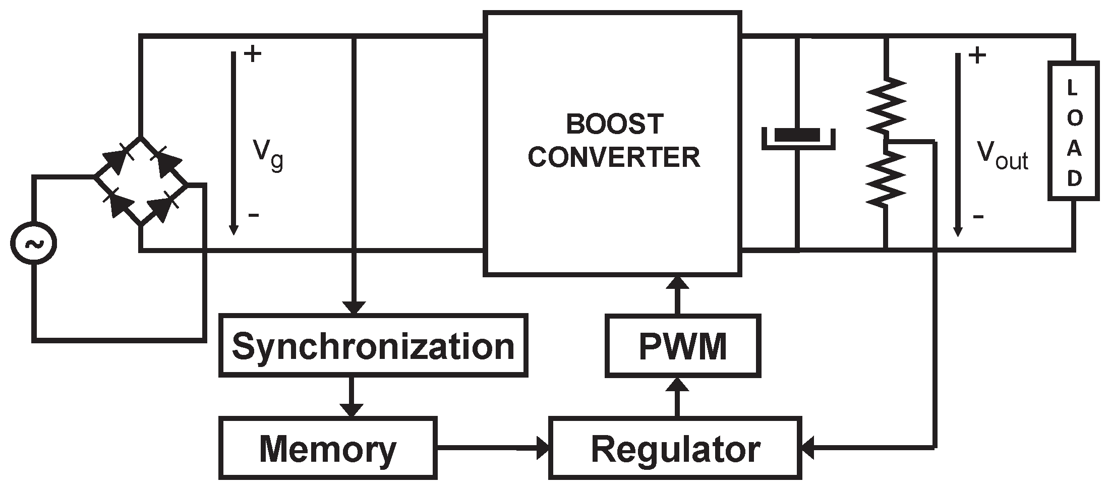
The proposed method detects leading or lagging currents without any current sensor and corrects them.
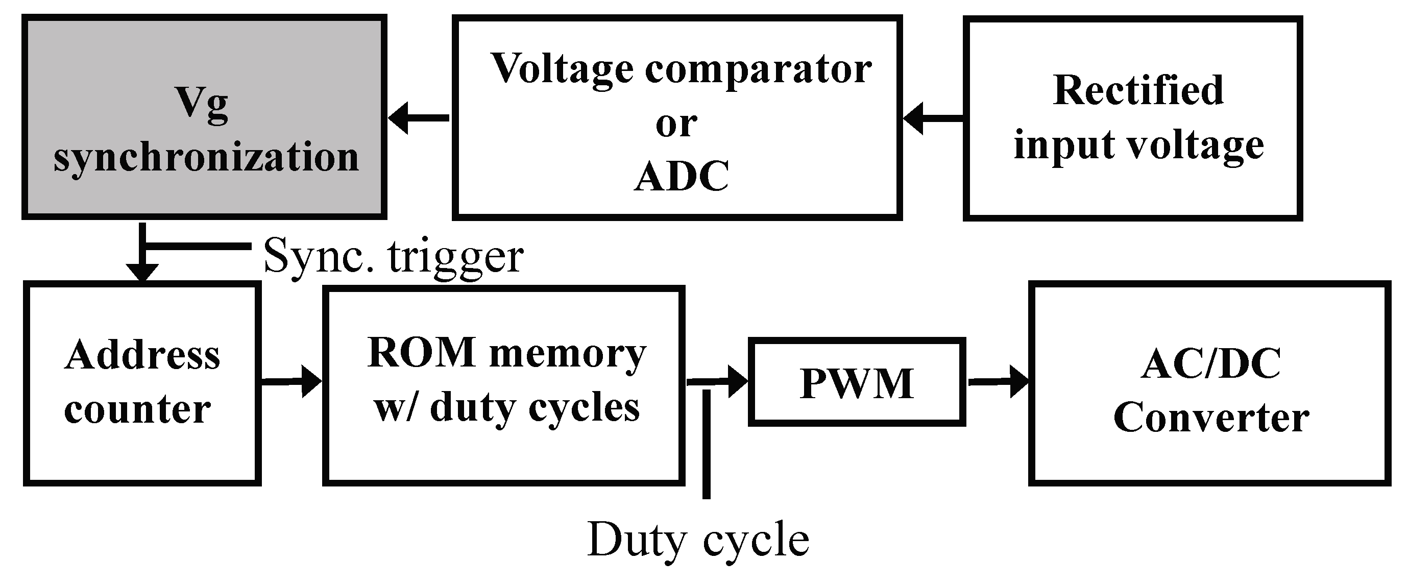
Figure 1 shows the high-level architecture of the proposed system. It can be seen that there is a memory with the precalculated duty cycles but they are regulated before being driven to the PWM generator. All the regulations are accomplished measuring only the output voltage. The synchronization method proposed in this paper also only uses the output voltage ADC, detecting the shape of the output voltage, which depends heavily on the input current.
As explained in the previous section, the main advantage of a system using precalculated duty cycles is to reduce the cost of the system by removing sensors, especially the current sensor. The precalculation should be accomplished taking into account the running conditions, i.e., the topology of the converter, the expected load, the input voltage, the input frequency, etc. In the case of a boost converter, the duty cycle during the ac period can be defined as follows, as can also be seen in [
33]:
In the previous equations, and are the input and output voltages, respectively, L is the inductance, is the inductor current, and is the switching period of the converter. These calculations can be done with high resolution or even adding other non-idealities such as losses, as they are performed offline with a computer. The system should only apply the precalculated duty cycles every line period. Nonetheless, the system should be able to modify in real time the precalculated duty cycles to adjust them to the actual conditions. Control loops should be added to modify the components of the duty cycle in case of non-nominal conditions.
The previous
parameter, as shown in Equation (
1), depends on the input voltage as well as the load through the ripple of the output voltage, thus it is not symmetric. It can not only be controlled by a classic output voltage loop, but also by a current regulation. To achieve both regulations,
can be divided into two components:
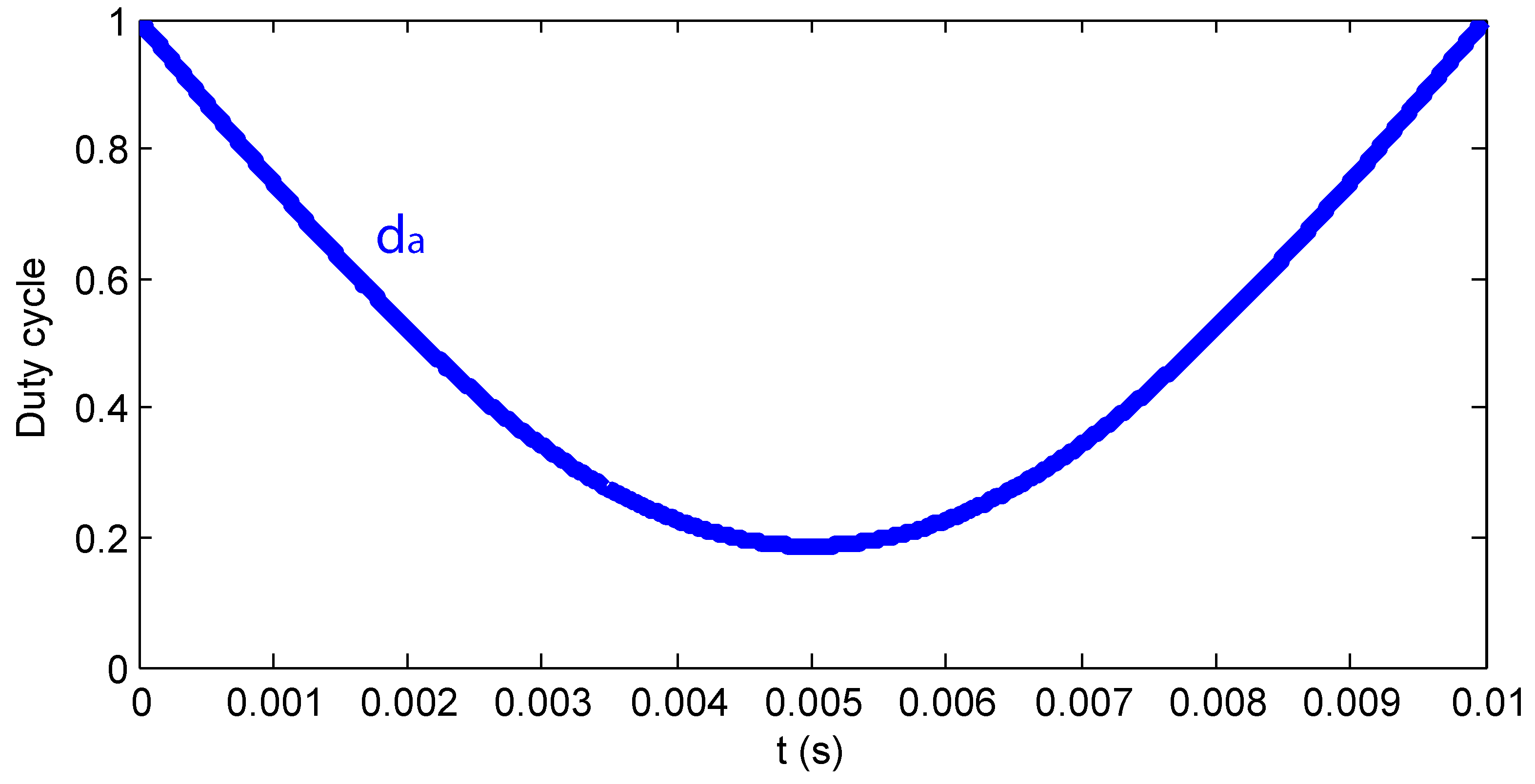
The parameter
defines the relationship between the instantaneous input voltage and the average output voltage. Hence, it does not depend on the load because the output voltage ripple is not considered, thus it is symmetric. As shown in
Figure 2,
is the main component of the total duty cycle.
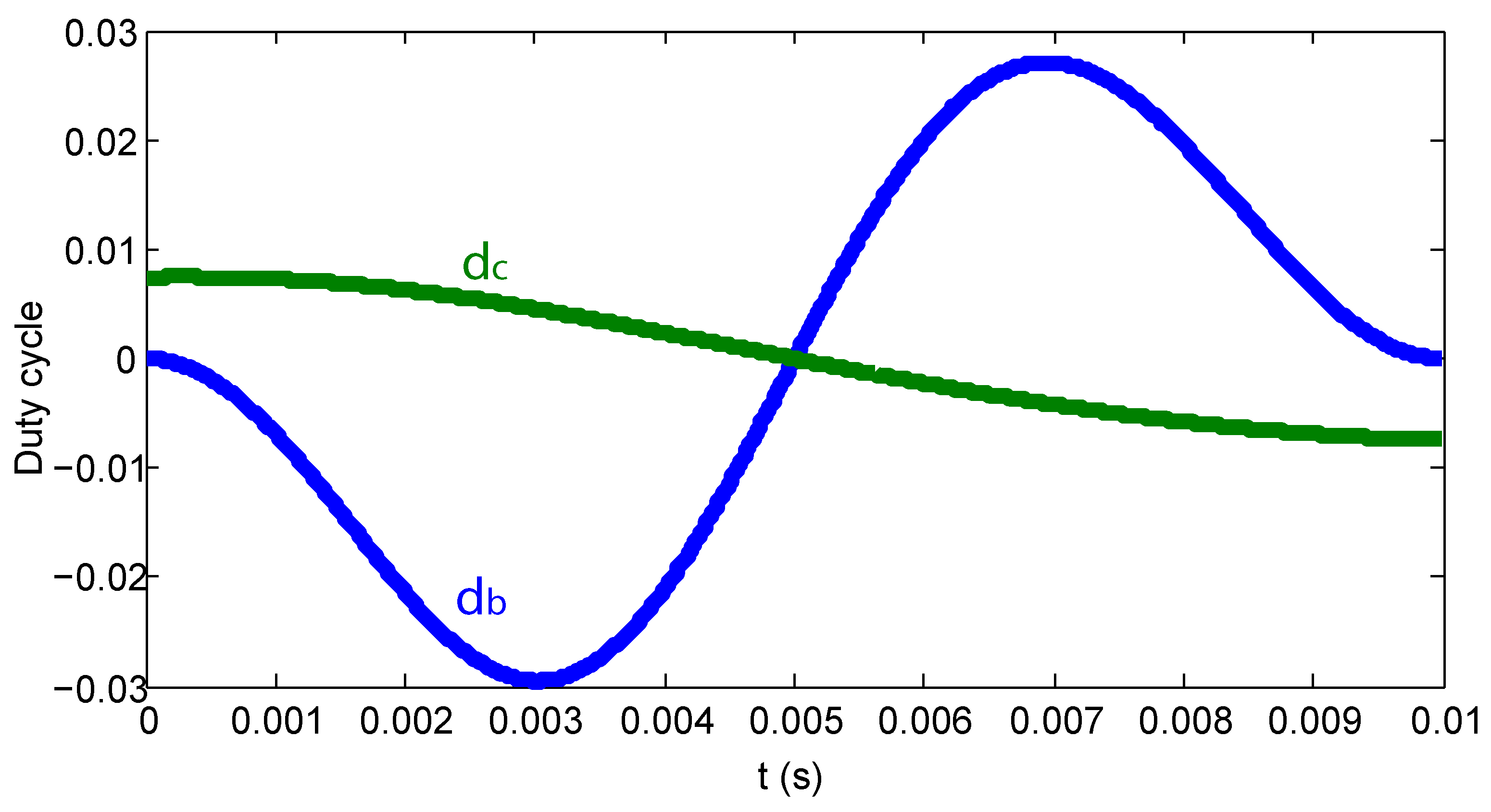
is the result of subtracting
from
, thus
takes into account the output voltage ripple produced by the load. As the output voltage is lower than the voltage average during the first half of the line period,
is negative, but
is positive during the second half as the output voltage is increased (see
Figure 3). Using
and
, the relation between voltages and the effect of the load are taken into account. Finally,
modifies the duty cycle to let the input current increase at the first half of the line period (positive values), while it decreases the input current at the second half of the line period (negative values). Therefore, the system gets the final duty cycle
d adding the components
,
and
:
A memory should store the values of
,
and
, and the controller will apply the output and current regulations for all the components.
and
should be regulated using the output voltage loop, which is a classic loop. On the other hand,
and
need to be regulated by the current regulation. This current regulation requires further description.
and
components depend on the input current and the input current is proportional to the input/output power of the converter for a given input voltage, so any change in the load would affect proportionally the input current and thus both components. The system cannot measure the power of the load directly, but it is able to extract that information from the ripple of the output voltage, which is already measured for the voltage loop. The ripple of the output voltage is proportional to the output power, thus, by sensing the ripple of the output voltage, both components can be regulated. This regulation measures the output voltage ripple but it does not try to modify it. It only adapts the waveform of the duty cycle—changing
and
—to improve the power factor when the load changes. However, the average values of the changed components (
and
) are 0 (as can be seen in
Figure 3), so the average output voltage will not be changed. Therefore, this regulation is not a typical closed loop, but a kind of feed-forward actuation. More details of the different duty cycle components can be found in [
33].
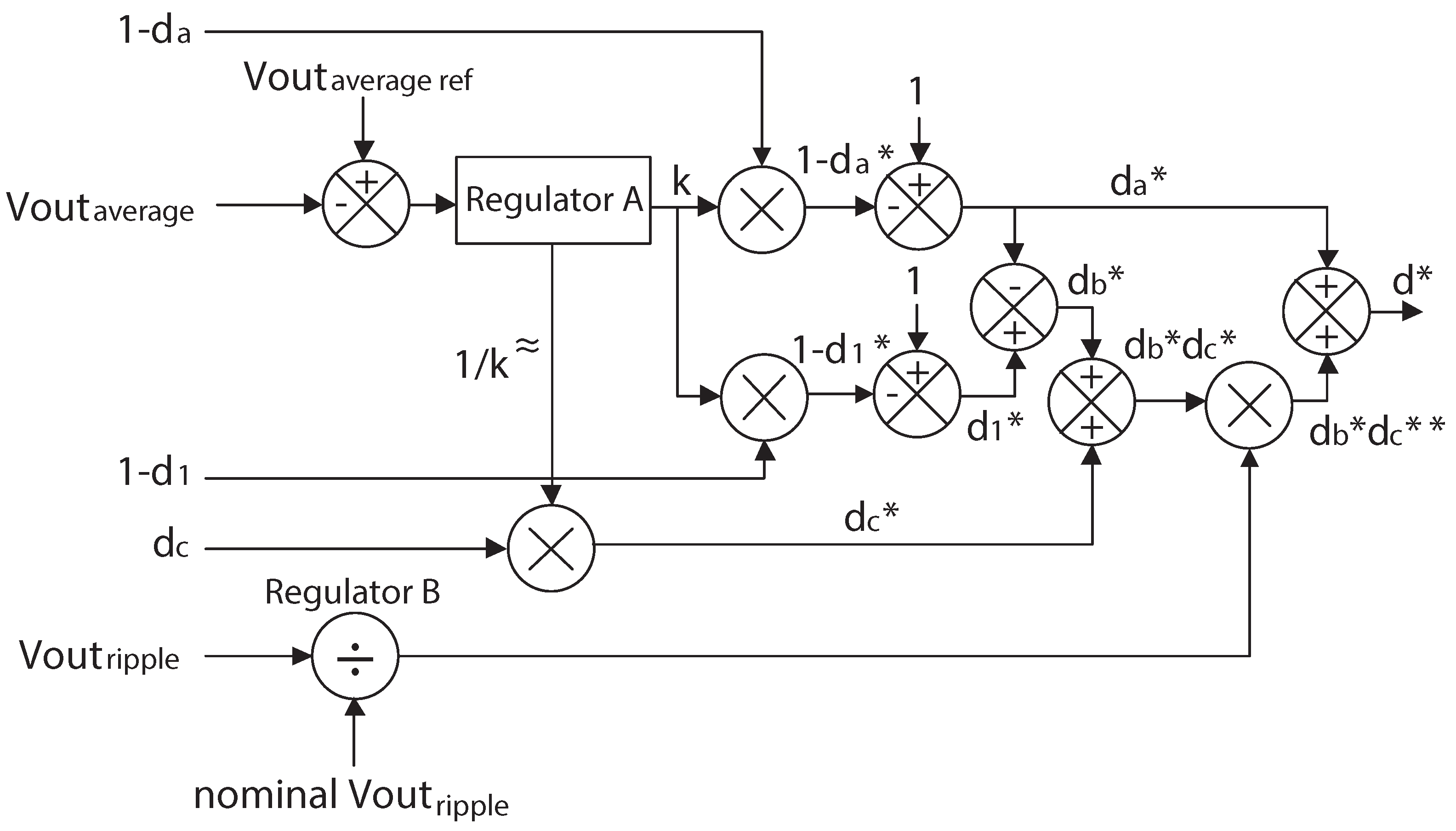
The regulation system proposed in [
33] is shown in
Figure 4. The figure shows two regulators that modify the duty cycles stored in the memories. The Regulator A reads the average output voltage during one cycle of the ac mains (
). Its actuation modifies the components
and
of the duty cycle. Likewise, the Regulator B reads the ripple of the output voltage during one cycle of the ac mains (
) and modifies the components
and
.
Table 1 shows the transfer functions of the regulators of
Figure 4. As can be seen, the sampling period of the regulators is 10 ms, as their inputs are updated every cycle of the ac mains. Regulator A is a PI (Proportional-Integral) regulator with a bandwidth of 3.7 Hz and its main objective is to compensate the differences between the real and the expected average output voltage. It has not been designed to get fast dynamics but to get a stable system. Regulator B implements a feed-forward regulator, in which actuation is proportional to the output voltage ripple, and its purpose is to adapt the duty cycle to non-nominal output loads. The measured output voltage ripple is divided by the nominal ripple (36.73 V) and the result is the actuation of Regulator B. That actuation is used to modify the components
and
, because they are proportional to the output load and, therefore, to the output voltage ripple. Further details about the regulators can be found in [
33].
With these two regulators, the system is able to get high power factor even under not nominal input voltages and under different loads. However, the system depends on the synchronization system with the ac mains, so any error in this process will worsen dramatically the power factor.
3. Detection of Synchronization Error and Regulation
As explained in the previous sections, a system based on precalculated duty cycles reduces the cost of the system but it depends on the synchronization. It is important to notice that, if the system is unsynchronized regarding the ac mains, it will apply wrong duty cycles, thus even small synchronization errors can lead to poor results.
An uncontrolled synchronization system can be implemented by measuring the rectified input voltage and detecting its periodical zero-crossing. This can be accomplished using an ADC or even with a voltage comparator (see
Figure 5). As can be seen, there is a ROM (Read Only Memory) memory with the duty cycles stored in it. Instead of storing the final duty cycle (
d), the components
,
and
are stored in three memories, as shown in
Figure 4. As the switching frequency of the system is 100 kHz and the ac mains frequency is 100 Hz, the memories will store 1000 duty cycles each one. Every component is written using 16 bits, where 11 bits are used to store a value between 0 and 999 in two’s complement, and 5 bits to store fractional values of the duty cycle components. These fractional values are used to implement a dither technique, which increases the resolution of the PWM [
35]. Hence, each component memory uses 16,000 bits, less than one block RAM of the FPGA used in
Section 4 (this low-cost FPGA provides 24 modules of 16 kb).
However, the synchronization process will present a latency caused by the ADC or the voltage comparator, i.e., the trigger. Besides, this process can be altered by noise in the measurement. Even when this latency is small, the power factor may be excessively reduced, because a system using precalculated duty cycles is very sensitive to this synchronization process.
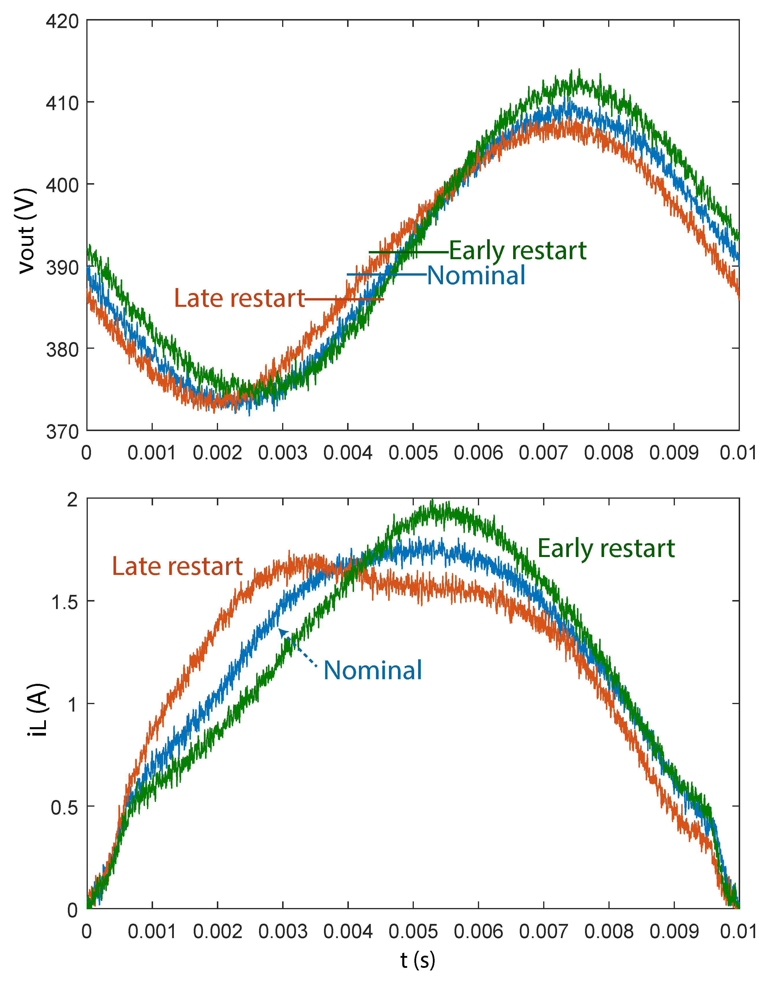
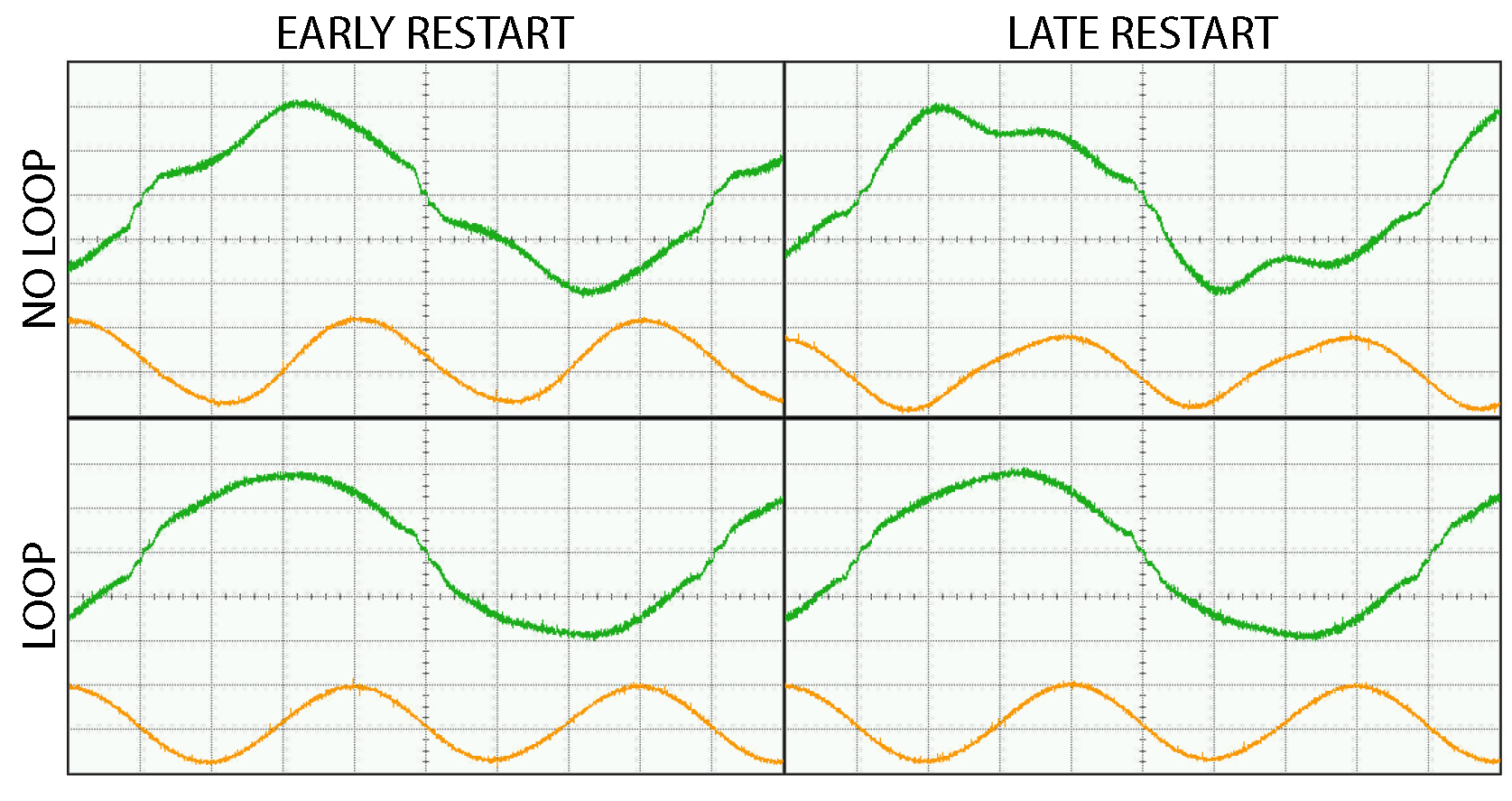
Figure 6 shows the output voltage and the input voltage when the synchronization process presents no delay, when there is an early restart of the counter of the memory and when there is a late restart. In
Figure 6, the positive and negative errors are 20 µs and −20 µs, respectively (±0.2% with respect to the ac semi-period). Using high speed ADCs and voltage comparators, the delay will be smaller, but also noticeable in the input current and, therefore, in the power factor. The graphics in
Figure 6 have been acquired from a real PFC corrector (see
Section 4) forcing the error cited above, and the switching noise has been reduced to clarify the figure.
As shown in
Figure 6, there is a relation between the input current and the output voltage. In the case of an early restart, the trough of the output voltage—its minimum value—appears after its ideal time, which is a quarter of the line period. Besides, its crest—its maximum value—also appears after its ideal time, which is three quarters of the line period. This effect is also known as lagging current, and it is also present in other PFC systems that do not measure the input current. In the case of a late restart, the behavior is the opposite: the trough and crest appear before the desirable time, which is also known as leading current. Besides, it can be seen that the crossing of the output voltage with the same value that in the origin of the line period,
, presents the same pattern: before in the case of the late restart, and after in the case of early restart. Lagging and leading current effects for a current sensorless PFC converter, which does not use precalculated duty cycles, is analyzed in [
23], where they prefer leading current than lagging current for their system to avoid hard-commutations currents. The technique proposed in this paper can be applied to any current sensorless PFC converter because they are always affected by leading or lagging currents, and this technique can regulate them through the ac mains synchronization.
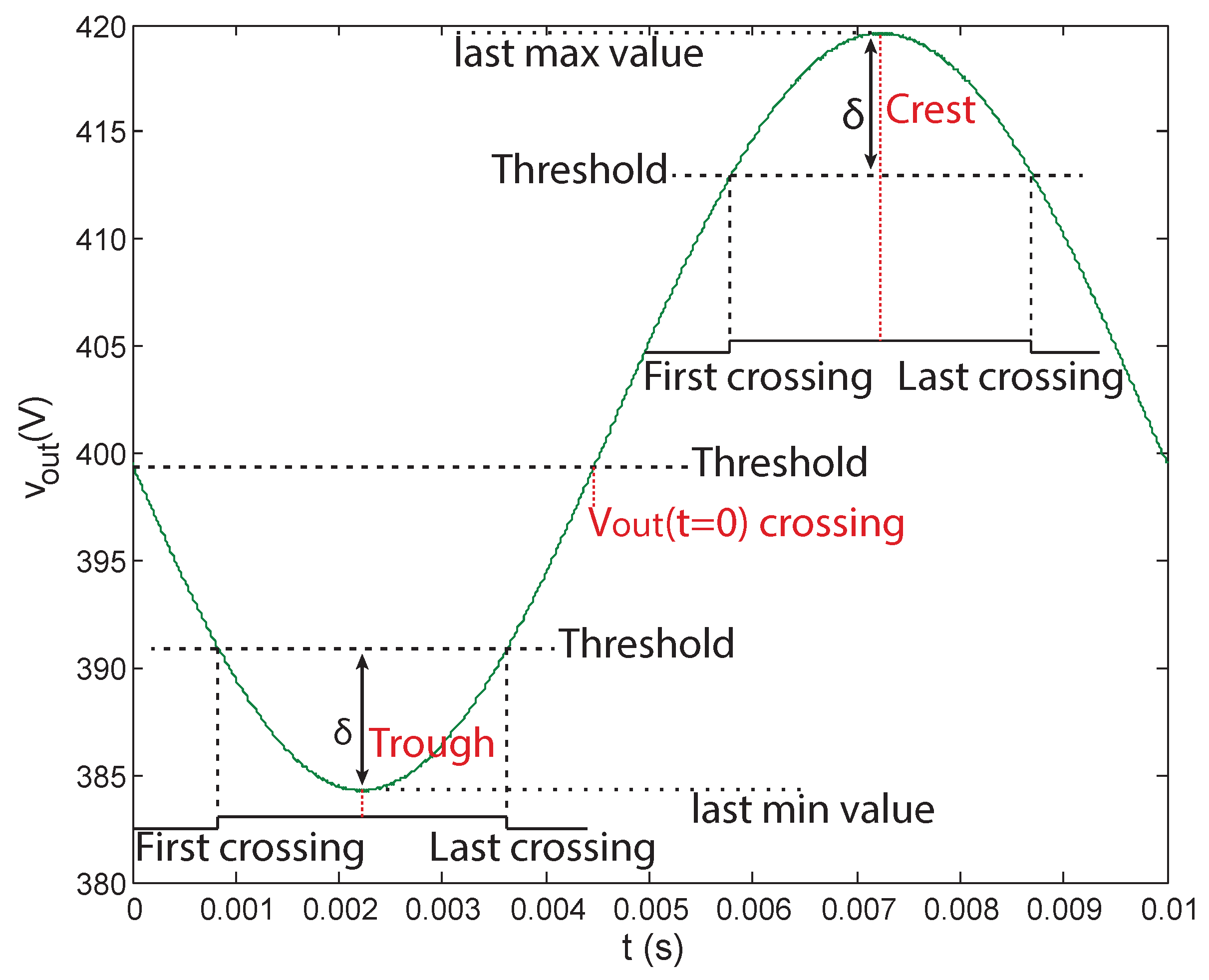
As explained above, there are three reference points that can be measured to detect synchronization errors: crest, trough and crossing. All these points can be detected using the same output voltage ADC of the two previous loops, thus the cost of the system is not increased.
Using an ADC is trivial to get the values of the output voltage, but it is not easy to detect the exact instant of the maximum and the minimum value. First, the output voltage has noise due to the switching converter, so the minimum or maximum values can be reached several times, because, in that zones, the derivative of the output voltage is near 0. This problem is increased if the resolution of the ADC is not enough to measure small increments in the output voltage. Besides, if the system is not well synchronized, the output voltage is not sine-shaped, thus there can be more than one maximum or minimum value.
This can be addressed by not detecting the crest or the trough, but the crossings with a threshold located near that crest or trough, as
Figure 7 shows. Near from the threshold, the derivative is bigger and the error in the detection method will be smaller. Considering both crossings (negative and positive), the system can measure the time between them and the half point between them it is the real crest or trough of the output voltage. This simple technique implicitly implements a low pass filter, so the error is reduced. However, the high frequency noise of the output voltage can produce multiple crossings, so the system will take into account only the first and the last crossing, as shown in
Figure 7. The threshold value is calculated by adding or subtracting a value,
, from the maximum or minimum value of the previous line period. This value,
, cannot be static because, in the case of the low loads, a static value of
could represent the whole ripple value. Therefore,
should be proportional to the ripple of the output voltage (in our case, 12.5% of the ripple value).
On the other hand, the detection of the other inflection point, i.e., the same value of the output voltage at the origin of the line period, is easier because in that point the derivative is in its maximum value and the electrical noise almost does not affect the measure of the output voltage. Therefore, this point is extracted by detecting the first crossing with the searched value.
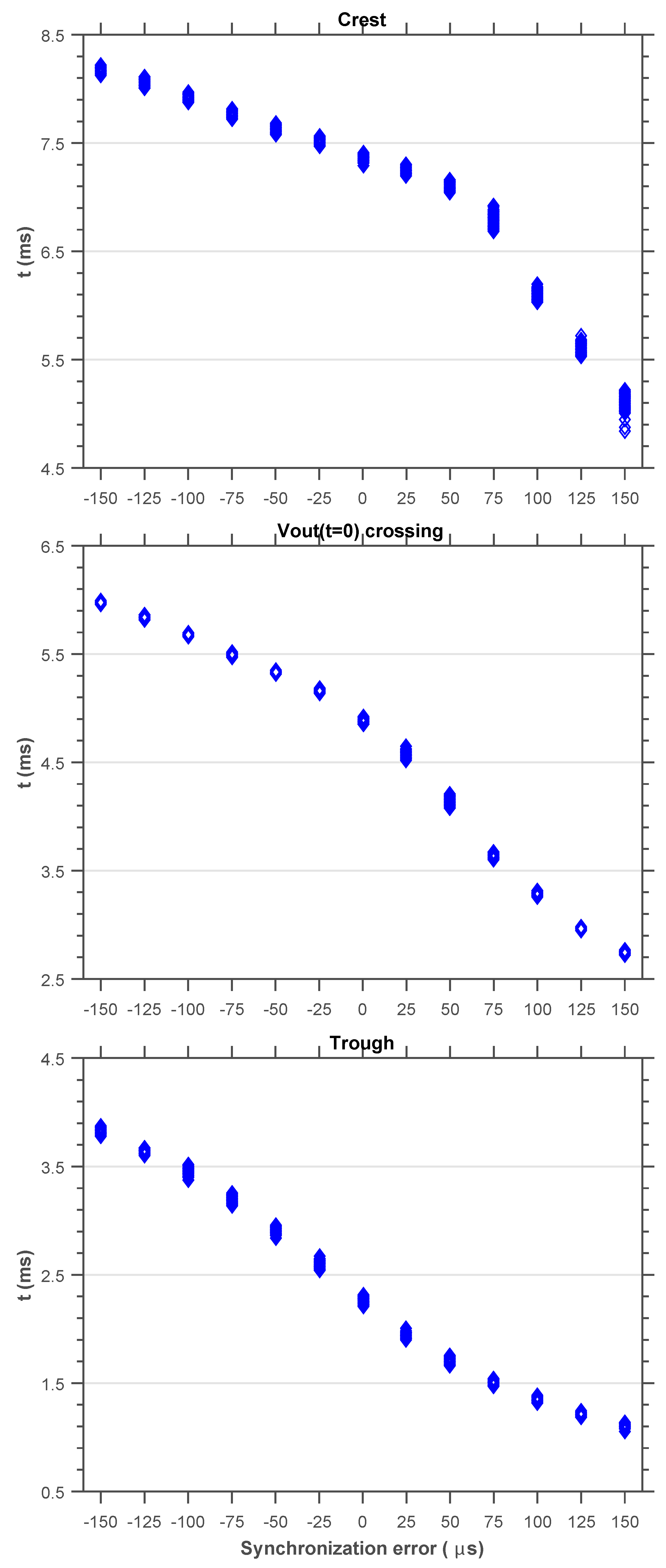
The mathematical relation between the synchronization error and the output voltage shape is very complex, so a traditional transfer function is not easy to extract. Therefore, a classic loop has not been implemented. As
Figure 5 shows, a system based on precalculated duty cycles generates a synchronization trigger, based on an analog measure of the input voltage and a digital synchronization system. The system proposed in this paper modifies the trigger generation, making the synchronization to trigger earlier or later, depending on the detected error (late restart or early restart, respectively). Before applying this simple technique, it has been experimentally proven that there is a nearly linear relation between the synchronization error and the positive or negative offset in the output voltage.
Figure 8 shows this almost linear relation for synchronization errors of ±1.5% of the ac period, and for all the characteristic points of the sine wave.
The synchronization loop output cannot be modified quickly because an abrupt change in the synchronization can lead to high currents and damage in the load or the converter, as it is a precalculated PFC. The method to make stable the synchronization loop is to choose a small positive or negative delay to add to the counter, which in our case is 20 ns (0.0002% of the line period). Therefore, the loop is very stable and it will slowly correct the error in the synchronization process. The loop slowness should not present big disadvantages because the error in the synchronization process (delay of the ADC/voltage comparator) is almost constant.
4. Experimental Results
The control methods proposed in the previous section were tested in an experimental setup. The explained PFC converter using precalculated duty cycles presents the parameters detailed in
Table 2. As can be seen, the inductance of the proposed system is quite high. As explained above, PFC systems that use precalculated duty cycles are quite sensitive to synchronization errors and other non-nominal conditions, and high inductors partially compensate this problem. In [
36], it is seen that selecting higher inductances allows systems without synchronization loop, such as the one proposed in this paper, to get better power factor and input current THD (Total Harmonic Distortion) when there are synchronization issues between the ac mains and the memory with the precalculated duty cycles. However, in [
36], it is seen that the capacitor value is not critical. Although this paper proposes a synchronization system that will avoid these issues, a high inductance, such as the ones used in precalculated PFC systems without synchronization loop, has been selected for a proper comparison.
The controller was implemented in a Xilinx FPGA XC7A100T-CSG324-3. The results of the following experiments were acquired with a Tektronix PA1000 power analyzer.
A simple control loop was implemented for every reference point of the output voltage waveform: crest, trough and the crossing with the same value of the output voltage at the origin of the ac semi-period (see
Figure 7). The control loop detected the time when these reference points occur and it compared them with their nominal values. Regarding the arithmetic sign of the comparison (positive or negative), the control loop generated the restart signal before or later.
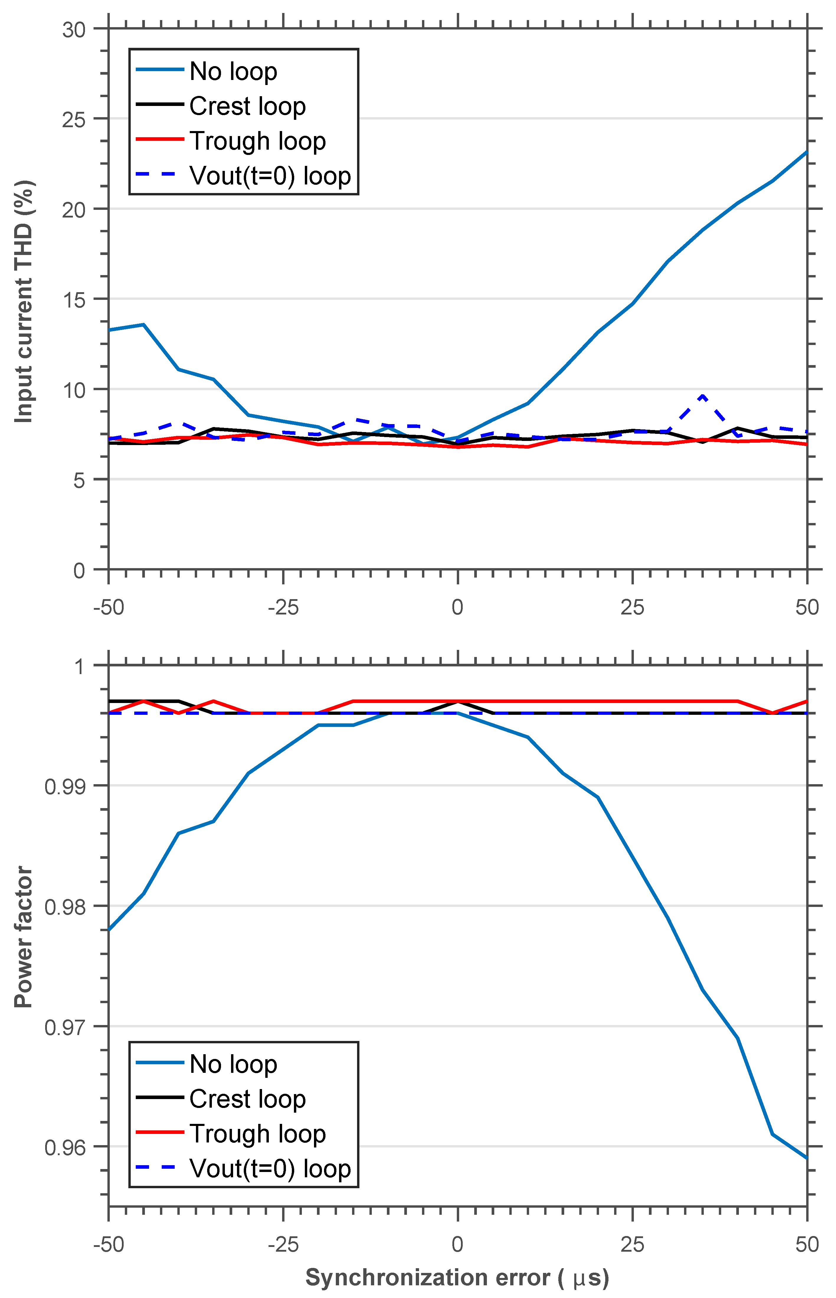
Figure 9 shows the results in terms of power factor and input current THD of the three proposed loops and the system without any regulation. It can be seen that the system with no synchronization loop cannot achieve high power factor under synchronization errors, both positive and negative. However, adding the synchronization loop, the converter keeps high power factor. As the previous figure shows, the choice between the different proposed loops is not quite relevant, because all the loops achieve approximately the same results.
As shown, the inclusion of a synchronization loop reaches high power factor under positive and negative synchronization errors. However, the logic complexity that is added with this loop should also be considered, because the precalculated approach is based on a low-cost goal.
Table 3 shows the resources used by the system with the different proposed synchronization loops and without them. It can be seen that the crest and trough loops use approximately the same number of LUTs (Look Up Table) and flip flops. This result was expected because both loops perform the same calculations using the crest or the trough of the output voltage signal (see
Figure 7). The Vout (t = 0) loop uses fewer resources because its complexity is lower, as it only detects a simple threshold crossing, without any arithmetic operations or filters.
Table 3 also shows the overhead produced by all the synchronization loops, in terms of absolute values and also percentages respect to the total LUTs and FFs. Comparing any proposed loop with the original system, it can be observed that the added complexity in terms of FPGA resources is small. The synchronization loop uses around 15% more resources than the original system but it should be noticed that the total logic size is really small. The PFC controller with the synchronization loop only uses 3% of the available programmable logic of the selected FPGA. Therefore, taking into account the loop complexity and the PF results, it is clearly proven that it is advantageous to include a synchronization loop in a PFC converter using precalculated duty cycles. All synchronization methods achieve good results but the trough loop, followed by the crest loop, gets the higher PF and lower current harmonics.
Figure 10 shows oscilloscope screenshots of the proposed system with and without the trough loop. Without the loop, the effects of lagging current (early restart) and leading (late restart) can be noticed. It can be seen also the correction of the synchronization loop, obtaining almost sinusoidal input current.
More experiments were performed to show the robustness of the proposed system.
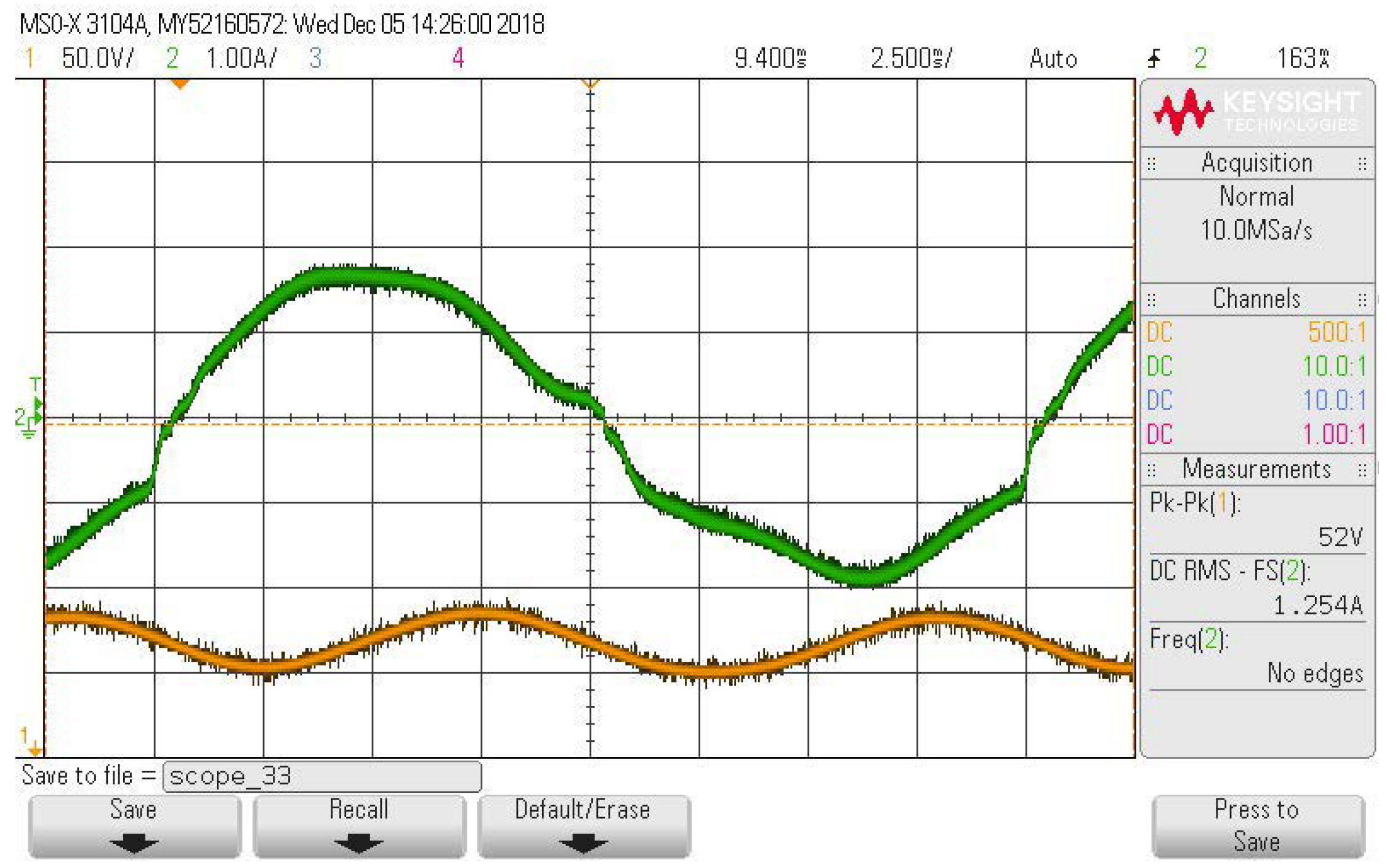
Figure 11 shows the output voltage and input current waveforms in nominal conditions. In that situation, the system reaches a power factor of 0.996 and an input current THD of 7.562%. Besides,
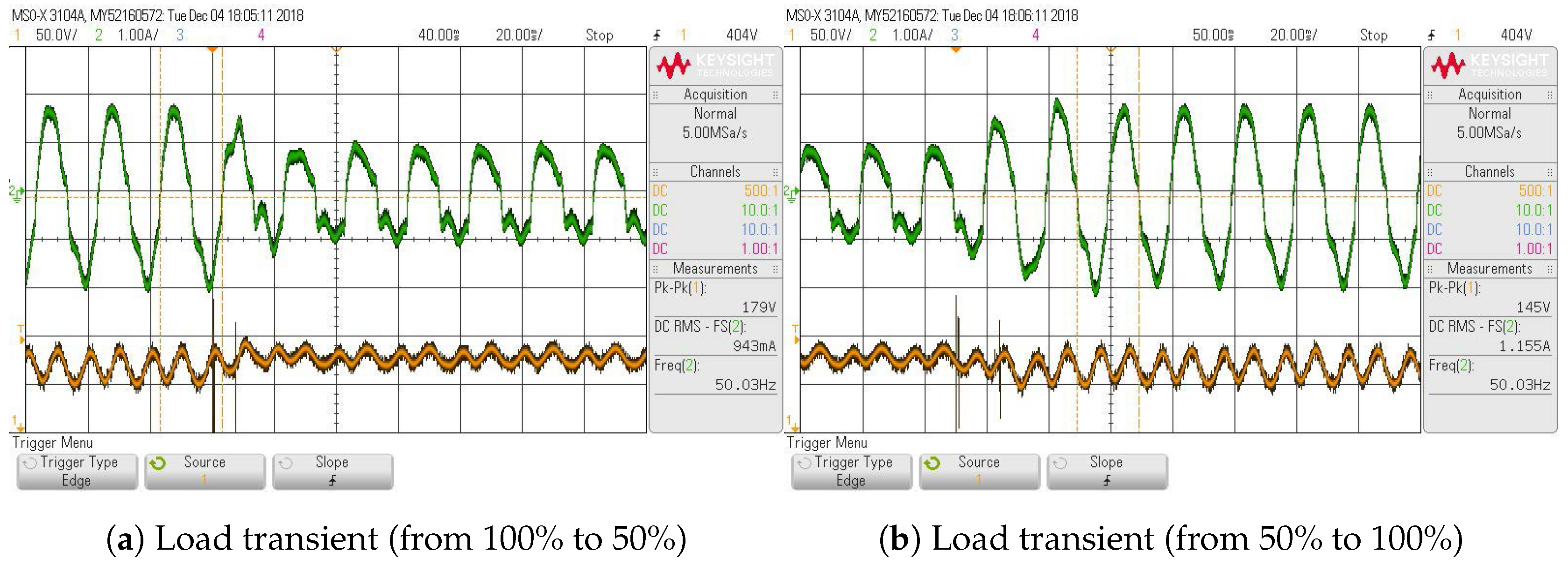
Figure 12 shows two load transients between 100% and 50% of load. It can be seen that the dynamic of the system is relatively fast, although this is not a primary goal. The reason is that the load change is easily and quickly detected by seeing the ripple of the output voltage. Therefore, Regulator B in
Figure 4 can quickly compensate the load change.
The previous experiments showed the behavior of the system with nominal input voltage. However, the system should work properly when the input voltage level and frequency are not as expected. In the case of the input voltage level, the system can handle the situation with the Regulator A of
Figure 4. However, as shown in [
37], systems that use precalculated duty cycles are very sensitive to frequency changes. In the system presented in this paper, a method to adapt the duty cycles to non-nominal ac frequencies has been included, such as the one presented in [
37].
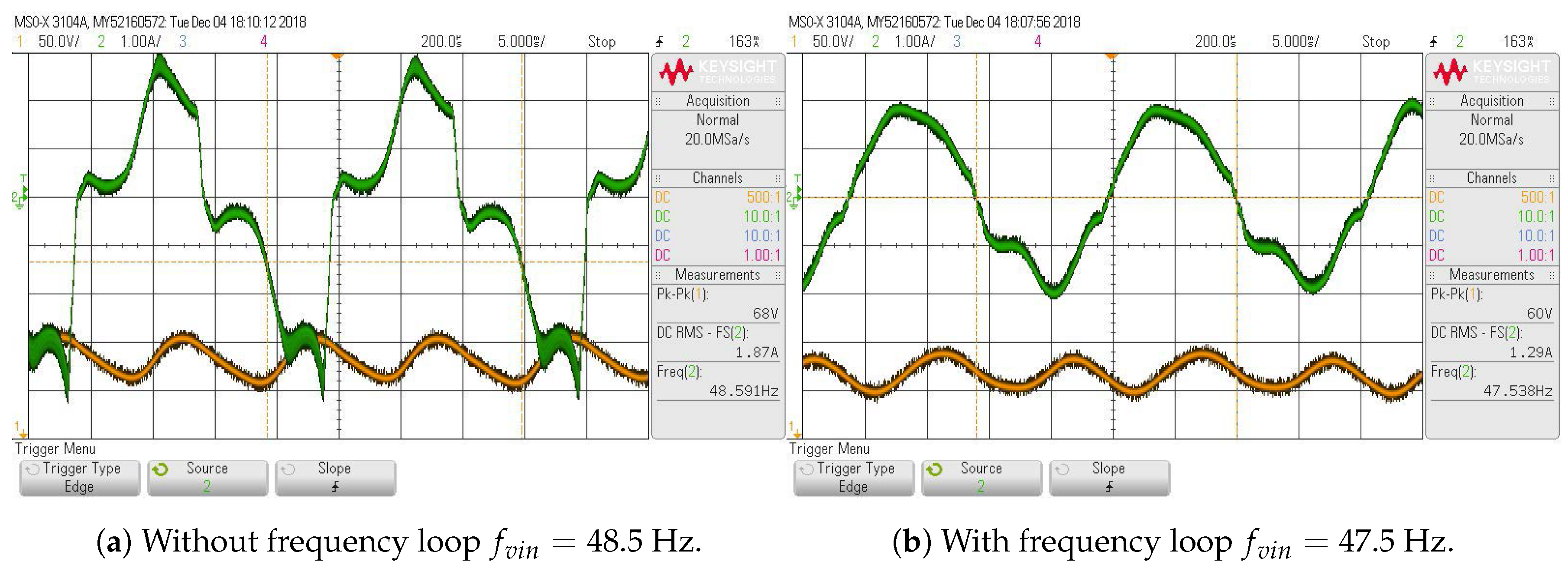
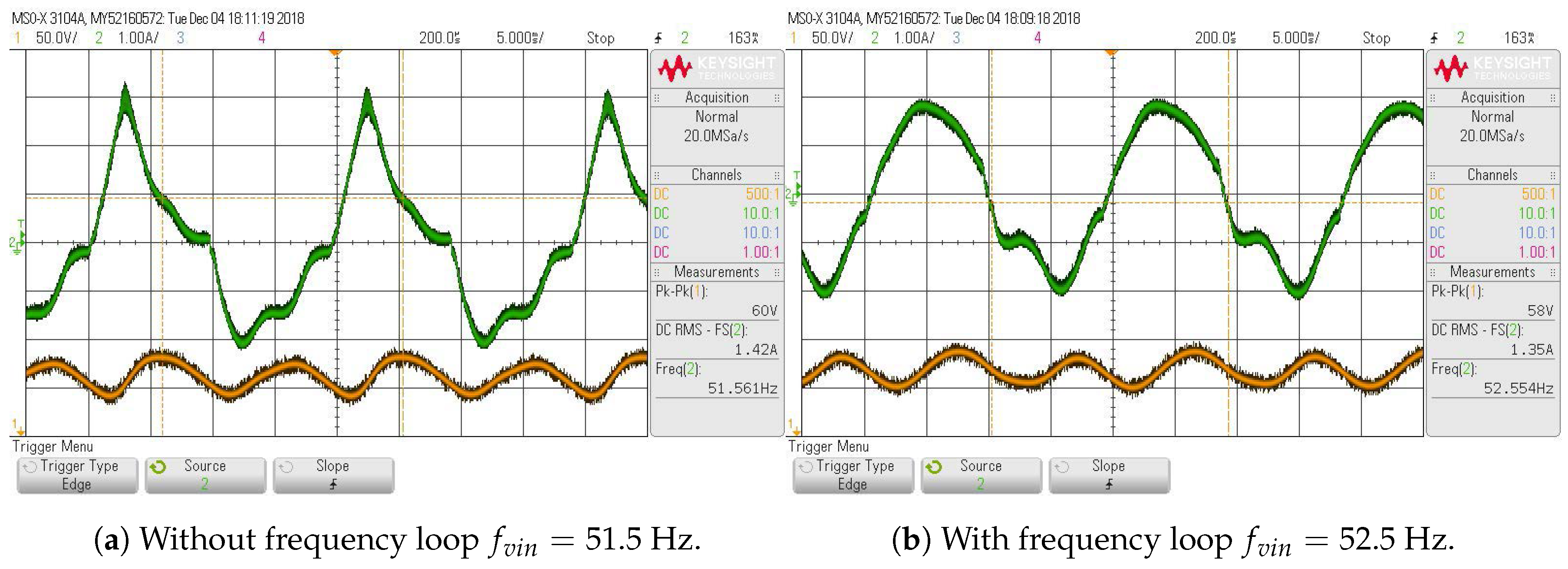
Figure 13 and
Figure 14 show the behavior of the system when the input voltage frequency is 47.5 and 52.5 Hz, with and without the frequency loop presented in [
37]. The system with the frequency loop gets a PF of 0.986 and input current THD of 6.876% when
Hz and a PF of 0.983 and input current THD of 8.899% when
Hz. However, without frequency loop, the system reaches a PF of 0.765 and input current THD of 39.15% when
Hz and a PF of 0.894 and input current THD of 27.87% when
Hz. These last results, without the frequency loop, are given for
Hz and
Hz instead of
Hz and
Hz, as the input current peaks trigger the protections. As a conclusion, it is important to include a control loop that measures the ac mains frequency, as the duty cycles precalculated should be applied in the expected moment.
All experiments show that a robust system can be implemented by measuring just the output voltage and a simple synchronization method with the ac mains.


