Article

A Methodology Improving Off-Chip, Lumped RF Impedance Matching Network Response Accuracy

by
Aleksandr Vasjanov
1,2,* and
Vaidotas Barzdenas
1,2
1
Department of Computer Science and Communications Technologies, Vilnius Gediminas Technical University, 10221 Vilnius, Lithuania
2
Micro and Nanoelectronics Systems Design and Research Laboratory, Vilnius Gediminas Technical University, 10257 Vilnius, Lithuania
*
Author to whom correspondence should be addressed.
Electronics 2018, 7(9), 188; https://doi.org/10.3390/electronics7090188
Submission received: 2 August 2018 / Revised: 1 September 2018 / Accepted: 8 September 2018 / Published: 10 September 2018

Abstract

:
Impedance matching is concurrent with any radio frequency (RF) circuit design and is essential for maximizing the gain and efficiency while minimizing the noise of high-frequency amplifiers as well as some mixer topologies. The main impedance matching network components are capacitors, inductors, and RF transformers all of which contain parasitic parameters that influence the matching response S11 curve. After calculating matching network component values using classical matching techniques, the measured and simulated response curves differ depending on the target frequency. This results in multiple calculations and measurement cycles in order to precisely match the source and load at the desired frequency. This article proposes an algorithm and methodology of estimating component parasitic parameters and taking them into account when calculating the main component parameters (capacitance and inductance). The proposed algorithm has been implemented as a toolbox in Cadence Virtuoso and verified through simulation and measurements. Measurement results show, that at 500 MHz 10% tolerance components with parasitics included and values based on classical theory provide a 3.2–9.8% offset from the target frequency. In the same conditions, matching networks with compensated (according to the proposed algorithm) values provide 0.1–8.8% target frequency offset. At 1500 MHz 10% components provided 4–12.3% (non-compensated) and 1–8.7% (compensated) target frequency offset ranges. At 3000 MHz. The frequency offset range of using compensated matching network component values is reduced from 5.5–15.1% to 1.3–8.1%.

1. Introduction

Impedance matching is concurrent with any radio frequency (RF) circuit design and is essential for maximizing the gain and efficiency while minimizing the noise of any high-frequency amplifier, either a low noise (LNA) or power (PA) amplifier, as well as some mixer topologies. The authors of [1] also contend that impedance matching as a key problem in RF circuit design and state that power losses of more than 1 dB when the matching quality degrades by 50%. This is an issue in QAM64 communication systems as they require power accuracy between channels of around 0.1 dB. For the maximum power transfer a condition has to be met, where load impedance ZL must be a complex conjugate of the source impedance ZS. Impedance matching networks have various shapes and implementations, including narrow- and wide-band; lumped, distributed, and mixed; and single- and multi-band. All of the latter configurations can provide an optimal solution depending on the design constraints (area, price, frequency, source, and load impedances). This article aims at improving the accuracy of impedance matching network response and proposes a methodology of recalculating the component values taking into account parasitic parameters.
In general, the main impedance matching network components are capacitors, inductors, and RF transformers (baluns) all of which contain parasitic parameters. After calculating matching network component values using classical matching techniques, the measured and simulated response curves differ depending on the target frequency. The deviation from the target frequency—the undesired offset of the S11 response on the frequency axis—depends on component parasitic parameters and tolerance as well as the target frequency. This results in multiple calculations and measurement cycles in order to match the source and load at the desired frequency. Component databases with parasitic parameters are available in different RF software tools, such as Advanced Design Systems (ADS) or Applied Wave Research (AWR) design environment, but their usage is the post-design phase of calculating impedance matching networks. As a result, this requires further optimization of the ideal calculated values.

Comparison to Existing Works

Different approaches aimed at improving impedance matching networks have been presented over the years. Paper [2] addresses parasitic parameter influence on impedance matching network response and proposes including ohmic losses in the design procedure. The authors provide equations which include the parasitic resistances of capacitors and inductors to match a real source with a complex load. This proposed approach has been confirmed effective for any two difference pair impedances to be conjugately matched. The impact of non-idealities of the lumped passive elements (inductor and capacitor) in the matching networks of RF amplifiers is analyzed in [3]. The authors described L-, π-, and T-networks by deriving expressions as a functions of inductor quality factor (QL), capacitor quality factor (QC), and transformation ratio. Simulation results show that a network synthesized on the basis of proposed set of equations nullifies the effect of non-idealities by 70–80% in L-networks and 10–20% in π-networks, but marginally improves the effect of non-idealities in T-networks at a frequency of 900 MHz. The authors of [4] provide and validate a methodology of calculating optimal impedance matching networks including the parasitics of on-board surface-mount components. The authors utilize ADS simulation capabilities in order to fine-tune the component values when using vendor-provided component databases and extracting printed circuit board (PCB) parasitics. Paper [5] proposes an algorithm of broadband matching with lumped elements. The authors provide an unusual way of designing the matching network by determining the back-end or front-end impedance of the matching network using the scattering parameters of the matching network, in conjunction with the source and load reflection coefficients. The scattering parameters of the matching network are optimized to be able to achieve maximum performance. The matching network itself is synthesized as a lossless two-port yielding the desired single matching network topology with initial element values. Paper [6] studies layout improvement techniques in order to obtain similar reflection and transmission responses when designing around 0402 and 0201 size components. The authors have improved the layout of 0402 size matching network by reducing land pad parasitics to obtain similar broadband characteristics to those when using 0201 parts. The authors of [7] study the Q-based approach of designing an impedance matching network. The Q-based approach is related to the energy transfer and dissipation in the matching network. Due to small losses in capacitors, the parasitic parameters of capacitor components are neglected; therefore the authors included only inductor parasitic parameters in their Q-factor-based approach.
Research on other types of matching networks have also been proposed including adopting a “CLCπ-type matching network for the purpose of making it variable [8], utilizing a micro-electro-mechanical system (MEMS) switch-based reconfigurable matching network to improve the linearity and efficiency of an RF power amplifier under load variations [9], and employing dual-band networks based on distributed components [10].
Most of the reviewed published articles on improving impedance matching accuracy proposed various methods of calculating lossless matching networks, and subsequently run computer-aided simulations including land pad and microstrip feed line electromagnetic co-simulation in order to fine-tune the results. Typically, only a single-case simulation of a matching network in one surface-mount package type is performed. None of the articles that are known to the authors include lumped component parasitic inductances and capacitances alongside with ohmic loss components. As a result this paper proposes a methodology of including lumped surface-mount component parasitic parameters such as equivalent series resistance (ESR), equivalent series inductance (ESL) and leakage resistance, all of which are based on the component value (capacitance or inductance), frequency, and surface mount device (SMD) package size. The proposed algorithm is the next step of optimizing calculated values based on classical impedance matching theory which can be integrated into the initial calculation stage. The latter algorithm is suitable for both narrow- and wide-band impedance matching networks and, for example, can be used with the wide-band matching network calculation methodology published in [5]. The proposed algorithm is discussed in detail in Section 2 of this article.

2. Proposed Impedance Matching Network Component Value Compensation Algorithm

The proposed impedance matching network synthesis (IMNS) algorithm is presented in Figure 1. The algorithm is intended to be used as a compensation technique after the impedance matching networks have been designed using classical matching techniques. The proposed algorithm is based on estimating surface mount device (SMD) component (capacitor and inductor) parasitics, such as Q-factor, ESR, ESL, self-resonant frequency (SRF), and drain resistance Rd, all of which are based on the component value (capacitance or inductance), frequency, and SMD package size. The need of compensation arises from the fact that the latter parasitic parameters shift the matching response (usually to the lower side of the frequency range) by a certain value, which is dependent on the target frequency. This frequency shift can reach several hundreds of megahertz. As a result, with no compensation techniques, the designer can match the network to the desired frequency only via several calculation and measurement cycles.
It is noted that parasitic inductance and capacitance for microstrip feed line going to and from the matching network can be included into the initial source and load impedances, and therefore the parasitic inductance and capacitance for the microstrip feed line are not mentioned in the proposed compensation algorithm. The microstrip lines connecting the matching network components together are neglected due to their minimal influence on the S11 response if the component layout has been done with careful consideration. The latter includes keeping minimal distances between matching network components and avoiding stubs. For example, a T-type matching network consisting of 0402 size components can typically have 0.5 mm microstrip transmission lines interconnecting the land pads and this distance introduces minimal impact up to 7.5 GHz. At this frequency, 0.5 mm becomes equal to λ/4 at which stage it will affect the response PCB dielectric with a permittivity of Er = 4. Although, when operating at higher frequencies the distance between components can be reduced or even select distributed component matching networks instead of those that utilize lumped components.
The proposed IMNS algorithm provides compensated matching network component values which match the source and load impedances at the desired frequency with improved accuracy compared to the classical matching theory.
The specific calculations that are required during each algorithm step are discussed in detail in the next section.

3. Proposed Impedance Matching Network Component Value Compensation Methodology

Different elaboration levels of lumped component models can be found in various references, but the approach proposed in this article utilizes lumped capacitor and inductor models with their respective parasitic parameters which are presented in Figure 2 [11]. The latter models have been selected as the estimated component parasitic parameters and equations presented in this article have been derived using the data presented by major capacitor and inductor manufacturers.
The lumped inductor model has the following parasitic parameters:
  • LPKG—SMD package equivalent series parasitic inductance, ESL;
  • R—SMD package series resistance, ESR;
  • CS—parasitic capacitance, which, alongside with L, defines SRF;
  • L—component inductance value.
Similarly, the lumped capacitor has the following parasitic parameters:
  • LPKG—SMD package equivalent series parasitic inductance, ESL;
  • RS—SMD package series resistance, ESR;
  • Rd = 1/Gd—capacitor parasitic drain resistance (or conductance Gd);
  • C—component capacitance value.
Lumped inductor model, presented in Figure 2a, has an equivalent impedance that can be split into resistance and reactance equations [11]. Solving equivalent reactance XL equation for component inductance L value provides a single real solution (1):
L = 4 C S 4 R 2 ω 4 X L 2 8 C S 3 R 2 ω 3 X L 4 C S 2 R 2 ω 2 + 1 2 C S ω X L 1 2 C S 2 ω 3 X L + 2 C S ω 2 .
The final value of the compensated inductor is found by subtracting the equivalent series parasitic package inductance LPKG from the result calculated in (1).
Similarly, lumped capacitor model, presented in Figure 2b, has an equivalent impedance that can be split into resistance and reactance equations [11] and solving equivalent reactance XC equation for component capacitance C value provides the following solution:
C = 4 G d 2 X C 2 8 G d 2 L PKG ω X C 4 G d 2 L PKG 2 ω 2 + 1 + 1 2 ω 2 X C 2 L PKG ω 2 .
Generalized inductor Q-factor has been derived as a polynomial function of frequency and inductance in the frequency range of 1 MHz–3 GHz for different package SMD inductors and is defined by the following equations:
Q ( f , L ) = n = 0 2 a n f n ,
a n = n = 0 2 b n L n ,
where an and bn are dimensionless coefficients, L depicts inductance in nH and f depicts frequency in Hz. Both equations are presented in a third order Taylor series form, providing the simplest yet sufficient estimate.
Various component manufacturers provide similar yet differing inductor Q-factor values, whereas Equations (3) and (4) provide a Q-factor value that is in the region of those that can be found on the market. The series could be expanded for a more accurate Q-factor curve which more closely corresponds to that provided by any single inductor manufacturer. Table 1 presents the derived dimensionless coefficient bn values for different size SMD inductors. The following values have been derived as a result of analyzing different SMD size Coilcraft [12] inductors in the frequency range of 1 MHz to 3 GHz.
SMD inductor SRF has been approximated as a function of inductance value by the following equation:
S R F 20 / L ,
where L is inductance in nH and SRF is in GHz. The latter equation has been derived by analyzing 0402HP series Coilcraft inductors [12] with values from 1 nH to 150 nH and curve-fitting the data to create a generalized equation. Inductor ESR (resistor R value in Figure 2a) is found from the following equation [13], which describes the relationship between Q-factor and reactance:
Q L = X L / E S R L .
Generalized capacitor ESR, has been derived as a polynomial function of frequency and capacitance in the frequency range of 1 MHz–3 GHz for different package SMD capacitors and is defined by the following equations:
E S R ( f , C ) = n = 0 2 m n f n ,
m n = n = 0 2 k n C n ,
where mn and kn are dimensionless coefficients, C depicts capacitance in pF and f depicts frequency in Hz. Similarly to Equations (3) and (4), Equations (7) and (8) are presented in a third order Taylor series form, providing the simplest yet sufficient estimate. Various component manufacturers provide similar yet differing capacitor ESR values, whereas Equations (7) and (8) provide an ESR value that is in the region of those that can be found on the market. The series could also be expanded for a more accurate Q-factor curve which closely corresponds to that provided by a single inductor manufacturer. Capacitor ESR estimation coefficients, presented in Table 2, have been derived by analyzing capacitors from two major capacitor manufacturers Murata [14] and TDK [15]. The analyzed capacitors had values of 0.1 pF, 0.5 pF, 1 pF, 5 pF, 10 pF, 18 pF, 20 pF, and 40 pF across 0201, 0402, 0603, 0805, and 1206 packages in a frequency range of 250 MHz to 3000 MHz in 250 MHz steps.
Larger size (0805 and 1206) capacitors have an almost identical ESR curve to that of 0603 capacitors. As a result coefficients for 0603 size capacitor can be used approximating ESR for both 0805 and 1206 size capacitors, hence are not included in Table 2.
Capacitor parasitic dielectric drain (leakage) resistance Rd = 1/Gd is dependent on the type of dielectric material used. The most widely used dielectric materials and their ESR and parasitic drain resistance Rd have been summarized analyzing [16,17,18,19] and are presented in Table 3.
SMD inductor and capacitor packages have typical ESL and ESR values that are presented in Table 4. The following parameters have been summarized by analyzing technical datasheets from different manufacturers [16,17,18,19,20].
The final compensated inductor or capacitor value is found by inserting reactance XL or XC, calculated using classical impedance matching theory, into (1) or (2) accordingly, taking into account the derived component parasitic parameter estimation Equations (3)–(8) and the coefficients (Table 1 and Table 2), typical SMD package parasitics (Table 3 and Table 4), and following the proposed algorithm in Figure 1.
It is to be noted, that the derived equations provide generalized lumped component model values that are suited not only to exactly describe Coilcraft, Murata or TDK components. The latter equations do not exactly match the parameter curves from the latter vendors, but provide a parameter change tendency, which is true to SMD capacitors and inductors in general, regardless of the manufacturer.
The proposed mathematical model and IMNS algorithm evaluation through simulation and measurement are presented in the following section.

4. Proposed Algorithm and Methodology Verification

The proposed impedance matching network synthesis algorithm has been implemented in Open Command Environment for Analysis (OCEAN) and Silicon Compiler Interface Language (SKILL) programming languages as a toolbox that can be integrated into Cadence Virtuoso design software.
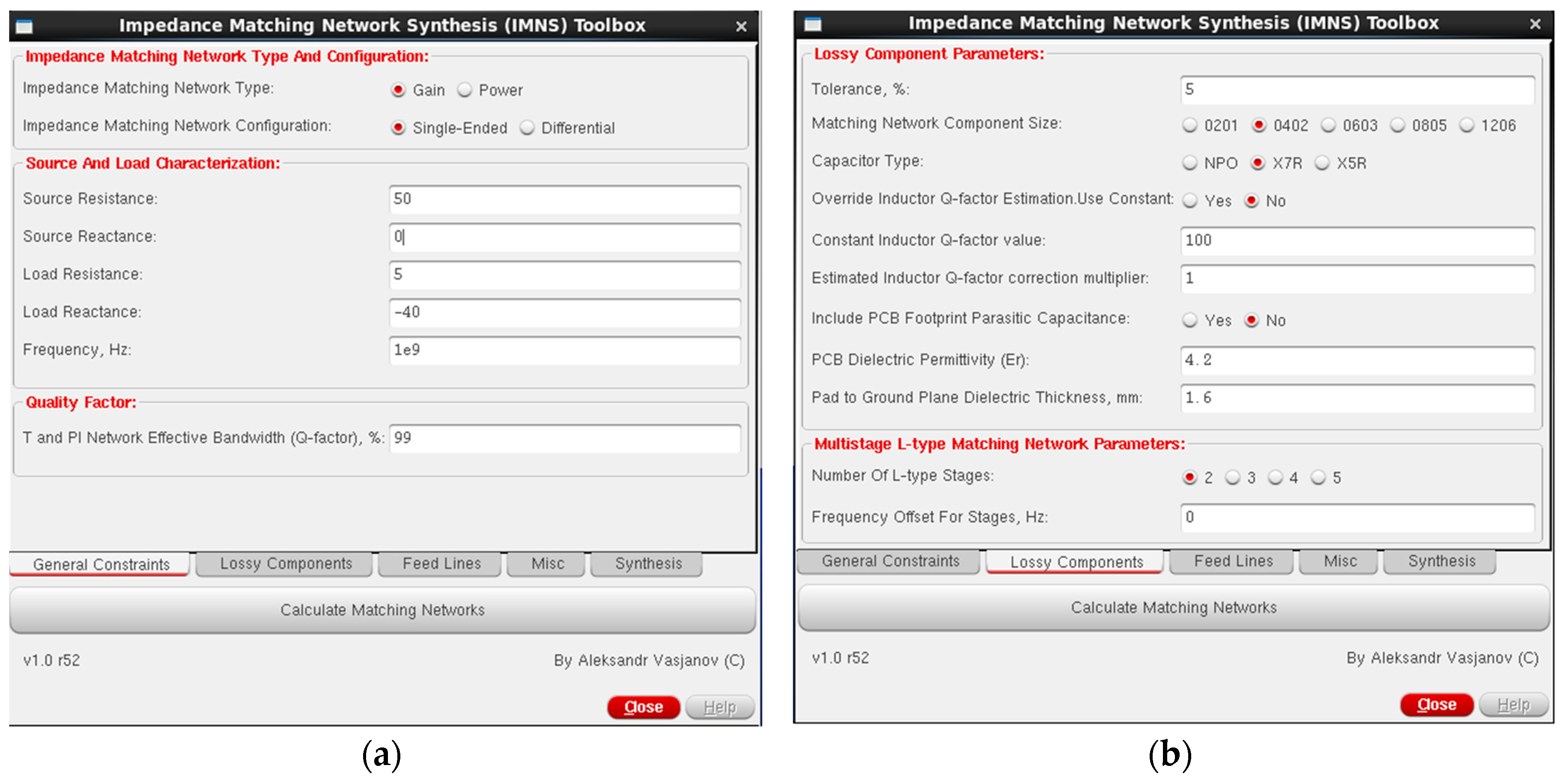
The two out of five toolbox tabs presented in Figure 3 are used to define the main impedance matching constraints and provide information on the type and size of SMD components. All of the latter information is taken into account when calculating the impedance matching network component values using classical theory and applying the proposed compensation methodology. The toolbox also provides an option to automatically synthesize all solutions in a selected Cadence Virtuoso library and evaluate each one running small-signal S-parameter simulations.
The proposed mathematical model and IMNS algorithm have both been evaluated via computer simulation and experimental measurements. Computer simulations have been conducted using the created IMNS toolbox in Cadence Virtuoso, whereas experimental measurements have been done using a calibrated HP8753E (Figure 4b) vector network analyzer (VNA) and an impedance controlled PCB. All measurement equipment has been calibrated using “Open/Short/Load” technique.
The verification procedure started with measuring the impedances of the device under test (DUT) at different frequencies resulting in the following load impedances: ZL,500MHz = 10.4 + j11.1, ZL,1500MHz = 14.6 + j36.6, and ZL,3000MHz = 54.3 + j111. Then L-type, π-type, and T-type matching networks, have been designed to match a source impedance of ZS = 50 Ω to measured load impedances using 0402 (the most widely used part sizes in the consumer electronics industry) size SMD components at 500 MHz, 1500 MHz, and 3000 MHz frequencies. Afterwards, all found solutions have been evaluated via computer simulation. The same network topologies with both ideal and compensated values according to the proposed methodology have been evaluated through measurement.
Results presented in Figure 5 plot three curves associated with each target frequency. “Sim. Non-compensated” curves (dotted) correspond to the simulation of matching networks with non-compensated component values, which are found using classical impedance matching theory, with all package parasitics included. “Meas. Non-compensated” curves (solid gray) correspond to measurement results, when closest to non-compensated component values, which are found using classical impedance matching theory, are used. Finally, “Meas. Compensated” curves (solid black) correspond to measurement results, when closest to the compensated component values, which have been calculated using the proposed methodology and IMNS algorithm, are used. Five attempts to match the source to the load at each target frequency have been conducted with consistent results using components from the same batch.
Figure 5a presents 0402 size L-type matching network simulation and measurement results accordingly at the frequency of 500 MHz. Ten percent tolerance SMD inductors and capacitors are used during experimental measurements. Analysis of the presented measurement results show that the impedance matching network with compensated values matches the source and load at a frequency of 504 MHz, when the target was 500 MHz. This proposed methodology minimizes the offset to 0.08% compared to 1% offset achieved with component values calculated using classical theory. Further analysis involves multiple impedance matching networks and the results reveal that at a target frequency of 500 MHz components with a 10% tolerance, parasitics and non-compensated values can introduce anywhere from 3.2 to 9.8% deviation from target frequency.
When using the same tolerance components at 500 MHz, matching networks with compensated values, the unwanted offset range becomes 0.1–8.8% from the target frequency. The proposed compensation algorithm reduced the worst case deviation by 1% at 500 MHz.
Figure 5b presents 0402 size T-type matching network simulation and measurement results accordingly at the frequency of 1500 MHz. Ten percent tolerance SMD inductors and capacitors were used during experimental measurements. The latter figure reveals smaller S11 value at the notch frequency, which is generally affected by the component tolerance and the closest available component values to the calculated ones.
Nevertheless, the proposed compensation algorithms matched the circuit at 1470 MHz compared to the 1440 MHz using the non-compensated values. This leads to a deviation improvement of 2.16%, from 4.16 to 2% deviation. Further insight into multiple matching networks at 1500 MHz revealed, that a 4–12.3% undesired offset from the target frequency can be introduced using 10% tolerance components using non-compensated values. Applying the proposed correction, the deviation region is reduced to 1–8.7% from the target frequency which is a 3.6% improvement at the worst case offset.
Figure 5c presents 0402 size T-type matching network simulation and measurement results accordingly at the frequency of 3000 MHz. Ten percent tolerance SMD inductors and capacitors are used during experimental measurements. The presented frequency responses conclude, that 10% tolerance components are not sufficient to provide exact (or within several percent of the target frequency) impedance matching at 3000 MHz. The compensated values improve the response and shift the curve from 2845 MHz to around 2900 MHz, but the target frequency is not reached. As a result, the deviation range of using compensated matching network component values reduces from 5.5–15.1% to 1.3–8.1% at a target frequency of 3000 MHz.
The results presented in Figure 5 have been obtained using components in listed Table 5. The number presented outside the brackets depicts the calculated value, while the value given inside the brackets is the closest manufactured component value to the calculated one. GRM155R71H series 0402 SMD capacitors and LQG15HS series 0402 SMD inductors, both manufactured by Murata, have been used during measurements. Components with the index “1” at the source side, whereas components with index “2” in the case of the L-type network and index “3” in the case of the T-type network—on the load side.
Due to the unknown exact value (including the deviation introduced by the component tolerance) of each component used, it is not clear what tolerance components are sufficient to provide accurate matching (within 1–2% of the target frequency). In order to find out whether or not 10% components can be used as matching network building blocks at high frequencies (2 GHz and above), a series of simulations have been conducted with the results presented in Figure 6 and Table 6.
An insight on a T-type matching network with 10% tolerance components at 2500 MHz target frequency is presented in Figure 5d. When all compensated component values (C = 14.38 pF, L = 3.15 nH, C = 0.59 pF) are reduced by 10%, the simulated response is as shown in the dotted line in Figure 5d alongside with the measured results. The fact that simulation results in Figure 5d are similar to the measurement results, implies that the lumped component models and the proposed parasitic parameter prediction algorithm performs with high accuracy and is viable when designing impedance matching networks. The measurement results in presented Figure 5d do not suffice the requirement to match the circuit at 2500 MHz due to low component tolerance. The latter leads to a statement, that in order to achieve high impedance matching network response accuracy (of around 1% at the target frequency), low tolerance components (5%, 2%, or even 1%) should be used alongside the proposed compensation algorithm that at high frequencies (above 2 GHz). At frequencies below 2 GHz, 10% tolerance components provide sufficient S11 curve accuracy.
The next logical step arising from the previous paragraph is to understand what component tolerance is sufficient at frequencies above 2 GHz. Component price is tightly related to its tolerance while reducing the cost of the bill of materials is paramount for high volume production.
A statistical yield analysis has been conducted on a T-type matching network at a target frequency of 2500 MHz with the results shown in Figure 6.
Each of the three graphs depicts the yield when one of the three component values has changed in the range related to the tolerance of the component. The selected number of samples was chosen to be 1000 and the target yield specification was chosen to be S11 ≤ −10 dB in the frequency range from 2400 MHz to 2600 MHz. Based on the results presented in Figure 6, component C3 (closest to the load) was the most susceptible to tolerance shifts and mostly defined the yield. In other words, the latter component introduced the most frequency shift to the S11 response. All three graphs in Figure 6 present components with 5% and 10% tolerances and one can clearly spot that at frequencies above 2000 MHz (in this case at a frequency of 2500 MHz) 10% tolerance components do not provide sufficient yield (above 95%) with the given target requirements.
Results presented in Table 6 are related to the histograms in Figure 6 and depict that 5% components provide a 99.3% yield at 2500 MHz. It has been mentioned that based on the results in Figure 6, component C2 value greatly affects the yield, and therefore the last row of the table displays a situation, when C2 tolerance is kept low (5%), but the tolerance of C1 and L1 is increased to that of standard general purpose components (20%). This resulted in a decrease in the yield only by 0.6%.
This leads to a conclusion that in order to have a ≥95% yield of matched circuits at a target frequency above 2000 MHz, 5% component tolerance is sufficient. An additional step can be taken to reduce the price of a mass-produced consumer product without sacrificing the yield. One can find the component in the matching network which is most responsible to the shift of the S11 curve in the frequency axis and replace this component with a 5% tolerant part while simultaneously reducing the tolerance of the rest of the matching network components to the cheapest 20% tolerance versions.
Figure 7 presents Monte Carlo simulation results for the matching network in 2.4–2.6 GHz frequency range. The latter figure presents histograms with minimal S11 response values (at the notch frequency) on the horizontal axis and the number of circuits that satisfy the latter condition on the vertical axis. Three types of component tolerances are used during Monte Carlo simulation and correspond to each histogram in Figure 7. The total area for each of the latter three histograms is identical. The histograms depict the number of circuits with different S11 response minimal value offsets from the target 2.5 GHz frequency due to component tolerance. According to the pink histogram that depicts the circuit performance with 10% tolerance components, in a lot of cases (181 out of 1000) the response is shifted in a way that S11 value shifts above the −10 dB threshold. This leads to a total yield of 81.9%, as presented in Table 6. In the case of 5% components, the number of failed circuits is less, resulting in negligible S11 curve shifts around the target frequency. As previously mentioned, in order to reduce the number of high tolerance components (and subsequently the overall price) without greatly affecting the S11 response and yield, the component that is most susceptible to value shifts (C2 in the case of Figure 6) is kept at 5% tolerance, whereas all other components are kept at a general purpose 20% tolerance level. According to the Monte Carlo simulation results that are shown in Figure 7, the red histogram spread is similar to the blue histogram in the frequency range of interest. This directly implies that the S11 curve frequency deviation is similar for matching networks with all 5% tolerance components to those with C2 at 5% and all other component tolerances kept at a general purpose 20%. Only a negligible number of occurrences when S11 > −10 dB in in both cases, resulting in a similar yield as provided in Table 6. The simulation results in Figure 6 confirm the proposition that in order to reduce the bill of materials (BOM) cost during mass production, only the most sensitive to change component in the impedance matching network needs to be high precision and all other component tolerances can be kept in the standard general purpose range.

5. Conclusions

Lumped impedance matching network components (capacitors and inductors) have parasitic parameters which affect the overall frequency response. Classical matching network design theory does not take them into account. As a result, a methodology of estimating the main parasitic component parameters as functions of surface mount device package size, frequency, and main parameter (capacitance or inductance) value alongside with a compensation algorithm has been proposed in this article. The proposed algorithm has been implemented as IMNS algorithm which has been further integrated as an IMNS Toolbox plugin into Cadence Virtuoso.
The proposed approach is based on an algorithm for predicting parasitic parameters of surface mount capacitors and inductors and recalculating the component value (capacitance and inductance). Impedance matching network component value tolerance is an important parameter which affects the accuracy of the S11 curve frequency response. Theoretical and experimental analysis of multiple impedance matching network results revealed that at a target frequency of 500 MHz components with a 10% tolerance, parasitics, and values based on classical theory (non-compensated) provide a 3.2–9.8% deviation from the target frequency. When employing the same tolerance components at 500 MHz, matching networks with compensated values (according to the proposed algorithm) provide a 0.1–8.8% target frequency offset. The proposed compensation algorithm reduced the worst case deviation by 1% at 500 MHz. The same components provided 4–12.3% (non-compensated) and 1–8.7% (compensated) target frequency deviation ranges at 1500 MHz. The deviation range of using compensated matching network component values is reduced from 5.5–15.1% to 1.3–8.1% at a target frequency of 3000 MHz. As a result, the proposed algorithm reduces the worst case frequency response offset by 1–7% compared to that of the classical theory. Experimental research results show, that 10% tolerance components can shift the S11 response by 1–5% at frequencies of up to 2000 MHz which can be held as sufficient, but more accurate value components are required at frequencies over 2000 MHz in order to obtain similar results.
According to the results obtained during statistical simulation and experimental research, 10% components provide a yield of only 81.9% within a 1000 samples the target specification of S11 ≤ −10 dB in the range from 2400 MHz to 2600 MHz. 5% tolerance components, on the other hand, provide a 99.3% yield in the same conditions. The improvements to the matching response accuracy using lower tolerance components (2% or 1%) compared to their unit price make their usage untenable compared to 5% tolerance components. An additional step can be taken to reduce the cost of a mass-produced consumer product while simultaneously maintaining a yield of 98.7%. First, find the component in the matching network that is most responsible for the shift of the S11 curve in the frequency axis and replace this component with a 5% tolerant part while simultaneously reducing the tolerance of the other matching network components to the cheapest 20% tolerance versions. On the other hand, lower tolerance components for all components of the matching network should be chosen if the budget is not of great importance and accuracy is the main priority.

Author Contributions

All authors contributed to the present paper with the same effort in finding available literature resources, conducting both simulations and measurements, as well as writing the paper.

Funding

This research was funded by the Research Council of Lithuania grant number DOTSUT-235, No. 01.2.2-LMT-K-718-01-0054 as a part of “Design and Research of Internet of Things (IoT) Framework Model and Tools for Intelligent Transport Systems” project. The APC was funded by Vilnius Gediminas technical university Faculty of Electronics.

Acknowledgments

The authors would like to thank the Research Council of Lithuania and the whole project “Design and Research of Internet of Things (IoT) Framework Model and Tools for Intelligent Transport Systems” team for their support, as well as John Liobe for observations while writing this paper.

Conflicts of Interest

The authors declare no conflict of interest.

References

  1. Mindan, B.; Hong, L. The Analysis of Impedance Matching Problem in RF Circuit Design. In Proceedings of the 2010 International Forum on Information Technology and Applications, Kunming, China, 16–18 July 2010; pp. 350–353. [Google Scholar]
  2. Yuan, Q.; Suzuki, S. Exact matching approach with circuit element ohmic loss. In Proceedings of the 2016 ISAP, Okinawa, Japan, 24–28 October 2016; pp. 342–343. [Google Scholar]
  3. Dasgupta, K.; Dutta, A.; Bhattacharyya, T.K. Parasitic aware impedance matching techniques for RF amplifiers. Analog Integr. Circuits Signal Process. 2012, 91–102. [Google Scholar] [CrossRef]
  4. Wang, T.; Michalka, T.; Luevano, G.R. Accurate and Efficient Impedance Matching Method in the Presence of on-board and SMT Parasitic Components. In Proceedings of the 2017 EPEPS, San Jose, CA, USA, 15–18 October 2017; pp. 1–3. [Google Scholar]
  5. Sengul, M. Broadband single matching with lumped elements. In Proceedings of the 2015 ELECO, Bursa, Turkey, 26–28 November 2015; pp. 115–1188. [Google Scholar]
  6. Luan, S.; Fan, J.; Knighten, J.L.; Smith, N.W. The design of a lumped element impedance-matching network with reduced parasitic effects obtained from numerical modeling. In Proceedings of the 2004 International Symposium on Electromagnetic Compatibility, Silicon Valley, CA, USA, 9–13 August 2004; pp. 984–987. [Google Scholar]
  7. Sun, Y.; Fidler, J.K. Practical considerations of impedance matching network design. In Proceedings of the 1994 Sixth International Conference on HF Radio Systems and Techniques, York, UK, 4–7 July 1994; pp. 229–233. [Google Scholar]
  8. Added, M.; Boulejfen, N. Variable impedance matching network based on varactor diodes. In Proceedings of the 2015 IEEE 15th Mediterranean Microwave Symposium, Lecce, Italy, 30 November–2 December 2015; pp. 1–4. [Google Scholar]
  9. Perez, C.S.; de Mingo, J.; Garcia-Ducar, P.; Carro, P.L.; Valdovinos, A. Optimization of the Efficiency and Linearity in RF Power Amplifiers under Load Variations using a Reconfigurable Matching Network. In Proceedings of the IEEE VTC-2010-Fall, Ottawa, ON, Canada, 6–9 September 2010; pp. 1–5. [Google Scholar]
  10. Maktoomi, M.A.; Panwar, V.; Hashmi, M.S.; Ghannouchi, F.M. A Dual-Band Matching Network for Frequency-Dependent Complex Loads Suitable for Dual-Band RF Amplifiers. In Proceedings of the 2014 IEEE IMaRC, Bangalore, India, 15–17 December 2014; pp. 88–91. [Google Scholar]
  11. Eroglu. Radio frequency amplifier basics. Practical resonances with loss, loading, and coupling effects. In Introduction to RF Power Amplifier Design and Simulation; CRC Press: Boca Raton, FL, USA, 2016. [Google Scholar]
  12. Coilcraft RF Inductor Finder. Available online: https://www.coilcraft.com/apps/finder/rffinder.cfm (accessed on 2 August 2018).
  13. Bowick, C. Impedance Matching in RF Circuit Design, 2nd ed.; Newnes: Newton, MA, USA, 2007. [Google Scholar]
  14. Murata GRM Series Capacitor Product Search and Characterization Tool. Available online: http://psearch.en.murata.com/capacitor/lineup/grm/#a02 (accessed on 2 August 2018).
  15. TDK MLCC Capacitor Product Search and Characterization Tool. Available online: https://product.tdk.com/en/search/capacitor/ceramic/mlcc/characteristic/ (accessed on 2 August 2018).
  16. Kemet Surface Mount Multilayer Ceramic Chip Capacitors (SMD MLCCs) Commercial Grade X5R Dielectric Datasheet. C1006_X5R_SMD. 29 November 2017. Available online: http://www.kemet.com/Lists/ProductCatalog/Attachments/19/KEM_C1006_X5R_SMD.pdf (accessed on 2 August 2018).
  17. Kemet Surface Mount Multilayer Ceramic Chip Capacitors (SMD MLCCs) Commercial Grade X7R Dielectric Datasheet C1027_X7R_COTS_SMD. 29 November 2017. Available online: http://www.kemet.com/Lists/ProductCatalog/Attachments/274/KEM_C1027_X7R_COTS_SMD.pdf (accessed on 2 August 2018).
  18. Parasitic Inductance of Multilayer Ceramic Capacitors by PhD J. Cain ACX Corporation. Available online: https://www.avx.com/docs/techinfo/CeramicCapacitors/parasitc.pdf (accessed on 2 August 2018).
  19. CDE Multilayer Ceramic Chip Capacitors—Performance Characteristics. Available online: http://www.cde.com/resources/catalogs/ceramperf.pdf (accessed on 2 August 2018).
  20. Intersil Application Note AN1325. 10 October 2011. Available online: https://www.intersil.com/content/dam/Intersil/documents/an13/an1325.pdf (accessed on 2 August 2018).
Figure 1. Proposed impedance matching network component value compensation algorithm.
Electronics 07 00188 g001
Figure 2. Lumped models: (a) inductor and (b) capacitor.
Electronics 07 00188 g002
Figure 3. Impedance matching network synthesis (IMNS) Toolbox tabs: (a) General Constraints and (b) Lossy Components.
Electronics 07 00188 g003
Figure 4. Proposed algorithm verification: (a) device under test (DUT) and (b) vector network analyzer (VNA) test-bench.
Electronics 07 00188 g004
Figure 5. Proposed algorithm verification results: (a) 0402 size L-type matching network research results at 500 MHz; (b) 0402 size T-type matching network research results at 1500 MHz; (c) 0402 size T-type matching network research results at 3000 MHz; and (d) 0402 size T-type matching network component tolerance evaluation results at 2500 MHz.
Electronics 07 00188 g005
Figure 6. Yield analysis of a matching network at 2500 MHz with different tolerance components: (a) Test circuit and load conditions; (b) component C1 value changed within tolerance with L1 and C2 values kept constant; (c) component L1 value changed within tolerance with C1 and C2 values kept constant; and (d) component C2 value changed within tolerance with C1 and L1 values kept constant.
Electronics 07 00188 g006
Figure 7. Monte Carlo simulation results in the frequency range of 2.4–2.6 GHz, when different tolerance matching network components are used.
Electronics 07 00188 g007
Table 1. Inductor Q-factor estimation for different surface mount device (SMD) packages.
0201 size
inductor
Coefficientb0b1b2
a05.7 × 10−20−4 × 10⁻¹⁹−4 × 10⁻¹⁸
a1−2.5 × 10−102.9 × 10−92.7 × 10−8
a2−9.7 × 10−21.044.5
0402 size
inductor
Coefficientb0b1b2
a01.04 × 10−205.2 × 10⁻²⁰−5.24 × 10⁻¹⁸
a1−6.86 × 10−112.57 × 10−94.47 × 10−8
a2−4.2 × 10−21.086.04
0603 size
inductor
Coefficientb0b1b2
a01.14 × 10−20−5.83 × 10−192.44 × 10⁻¹⁸
a17.27 × 10−11−2.31 × 10−95.08 × 10−8
a22.46 × 10−2−8.52 × 10−112.8
0805 size
inductor
Coefficientb0b1b2
a01.7 × 10−20−1.48 × 10⁻¹⁸−5.92 × 10⁻¹⁸
a1−3.37 × 10⁻¹²−2.69 × 10−107.78 × 10⁻⁸
a22.08 × 10−31.17 × 10−111.76
1206 size
inductor
Coefficientb0b1b2
a02.48 × 10−21−2.5 × 10⁻¹⁹−1.7 × 10⁻¹⁷
a11.13 × 10−12−6.23 × 10−108.16 × 10⁻⁸
a2−4.63 × 10−38.35 × 10−110.4
Table 2. Capacitor equivalent series resistance (ESR) estimation for different SMD packages.
0201 size
capacitor
Coefficientk0k1k2
m0−7.22 × 10−243.83 × 10−228.4 × 10⁻²²
m1−6.01 × 10−141.49 × 10⁻¹²−3.44 × 10⁻¹²
m24.71 × 10−3−1.31 × 10−19.09 × 10−1
0402 size
capacitor
Coefficientk0k1k2
m0−2.66 × 10−237.31 × 10−221.93 × 10⁻²¹
m1−7.94 × 10−142.99 × 10⁻¹²−5.07 × 10⁻¹²
m24.84 × 10−3−1.35 × 10−18.93 × 10−1
0603 size
capacitor
Coefficientk0k1k2
m0−3.95 × 10−232.44 × 10⁻²¹−2.3 × 10⁻²⁰
m12.05 × 10−13−1.26 × 10−111.75 × 10⁻¹⁰
m22.6 × 10−4−1.51 × 10−23.86 × 10−1
Table 3. SMD capacitor parasitic drain resistance.
Dielectric TypeRd, GΩ
NPO/C0G100
X7R100
X5R50
Table 4. Typical equivalent series inductance (ESL) and ESR for different SMD packages.
PackageESL, pHESR, mΩ
020140040
040255049
060370077
080580067
1206125099
Table 5. 0402 size impedance matching network component values.
0402 Matching Network TypeMatching Network Component Values
500 MHz1500 MHz3000 MHz
L-, T-typeNon-compensatedForward L-type T-typeT-type
(L-shunt, C-series)C1 = 17.7 (18) pFC1 = 3.58 (3.6) pF
L1 = 7.86 (8.2) nHL2 = 3.18 (3.3) nHL2 = 8.58 (8.2) nH
C2 = 11.43 (11) pFC3 = 1.78 (1.8) pFC3 = 0.47 (0.5) pF
CompensatedForward L-typeT-typeT-type
(L-shunt, C-series)C1 = 10.67 (11) pFC1 = 2.3 (2.2) pF
L1 = 7.47 (7.5) nHL2 = 2.78 (2.7) nHL2 = 6.83 (6.8) nH
C2 = 10.87 (11) pFC3 = 1.69 (1.6) pFC3 = 0.45 (0.5) pF
Table 6. Yield results at 2500 MHz target frequency.
Yield, %Number of Passed/Failed CircuitsTarget Specification/Comment
81.9819/181All components 10%, S11 ≤ −10 dB in the range on 2400 MHz–2600 MHz
99.3993/7All components 5%, S11 ≤ −10 dB in the range on 2400 MHz–2600 MHz
98.7987/13C2 tolerance 5%, C1 and L1 tolerance 20%, S11 ≤ −10 dB in the range on 2400 MHz–2600 MHz

