Article

Comparative Evaluation of Three-Phase Three-Level Flying Capacitor and Stacked Polyphase Bridge GaN Inverter Systems for Integrated Motor Drives

1
Power Electronic Systems Laboratory, ETH Zurich, 8092 Zurich, Switzerland
2
Innsbruck Drives and Energy Systems Laboratory, University of Innsbruck, 6020 Innsbruck, Austria
*
Author to whom correspondence should be addressed.
Electronics 2024, 13(7), 1259; https://doi.org/10.3390/electronics13071259
Submission received: 23 February 2024 / Revised: 18 March 2024 / Accepted: 22 March 2024 / Published: 28 March 2024
(This article belongs to the Section Power Electronics)

Abstract

:
This article presents a comprehensive comparative evaluation of a three-phase Three-Level (3L) Flying Capacitor Converter (FCC) and a Stacked Polyphase Bridge Inverter (SPBI), specifically a converter system formed by two Series-Stacked Two-Level three-phase Converters (2L-SSC), for the realization of a 7.5 kW Integrated Motor Drive (IMD) with a high short-term overload capability. The 2L-SSC requires a motor with two three-phase windings and a split DC-link, but uses standard six-switch, two-level transistor configurations. In contrast, the bridge legs of the 3L-FCC feature flying capacitors whose voltages must be actively balanced. Despite the 800 V DC-link voltage, both topologies employ the same set of 650 V GaN power transistors, i.e., the same total chip area, and if operated at the same switching frequency, show identical semiconductor losses. Electric Discharge Machining (EDM) damage of the motor bearings is a relevant issue caused by the common-mode (CM) voltages of the inverter stage. The high effective switching frequency of the 3L-FCC and the possibility of CM voltage canceling in the 2L-SSC facilitate mitigation of EDM by means of CM chokes, whereby a substantially smaller CM choke with lower losses suffices for the 2L-SSC; based on exemplary designs, the 2L-SSC features only about 75% of the total volume and 85% of the nominal losses of the 3L-FCC. If, alternatively, motor-friendliness is maximized by including DC-referenced sine-wave output filters, the 3L-FCC’s higher effective switching frequency and the 2L-SSC’s need for two sets of filters due to the dual-winding-set motor change the outcome. In this case, the 3L-FCC features only about 60% of the volume and only about 55% of the 2L-SSC’s nominal losses.

1. Introduction

In recent years, a trend towards Integrated Motor Drive (IMD) systems has evolved, eliminating the need for (expensive) shielded cables between the drive and the motor and facilitating more compact arrangements of the Variable Speed Drive (VSD) and the motor as single units [1]. Expedient for this development, an increasing interest from industry in local DC distribution grids, i.e., several VSDs are supplied from a common DC bus, has emerged, e.g., with DC-link voltages of up to 800 V to lower the DC cabling cross-section. Advantageously, then only the DC–AC inverter stage (but no AC–DC rectifier stage) has to be integrated into the motor [2].
Compared to standard two-level inverters, implementing the motor drive as a multi-level inverter with a higher effective switching frequency and lower voltage steps at the switch-node output benefits the motor with reduced output voltage harmonics and lower winding voltage stresses [3,4]. Typically, three-level topologies are employed, as more levels lead to significantly higher complexity [5]. Prominent three-level topologies are, first, T-type concepts that, however, employ two different types of transistors (i.e., with different voltage blocking capabilities) [3,6]. Second, diode-clamped structures like the neutral-point-clamped (NPC) converter [7,8], or, replacing the diodes with transistors, active NPC (ANPC) bridge legs are widely used in high-power applications. However, there, six instead of only four power semiconductors per bridge leg are needed.
Finally, using capacitors for defining additional voltage levels, the Three-Level Flying Capacitor Converter (3L-FCC) shown in Figure 1a features bridge legs with only four transistors of a single type, which are further equally stressed in a steady-state operation. Specifically, an 800 V DC-link system can be realized with the latest 650 V GaN power semiconductor technology, featuring low chip area, low on-state resistance ( R dson ), and low switching losses. This facilitates a small inverter stage footprint and a high power conversion efficiency, that are both fundamentally important for the motor integration of the inverter.
However, for these FCC topologies, as shown in [5], overload operation requirements, such as three times the rated torque for 3 s as expected from motor drives in, e.g., servo applications [9], can only be handled with relatively large Flying Capacitors (FCs) to keep the maximum FC voltage ripple amplitude and/or the losses per capacitor below the design limits. The latter can be avoided by increasing the switching frequency in overload periods, which, however, increases the implementation complexity. Moreover, the FC voltages might require active control due to shortcomings in the natural balancing behavior when operated with, e.g., non-ideal source impedances, gate drive delays, and input voltage startup/fluctuations [10,11,12], which adds to the previously mentioned complexity.
Accordingly, alternative inverter concepts are of interest, such as the Stacked Polyphase Bridge Inverter (SPBI), as follows: In the case at hand, two three-phase two-level inverter stages are stacked, i.e., connected in series on the DC input side and each inverter stage supplies an individual three-phase winding set of the motor (cf. Figure 1b) [13,14,15,16,17,18,19]. Advantageously, such a 2L-SSC with an 800 V DC input can also employ latest 650 V GaN semiconductors configured in standard two-level half-bridge arrangement, and requires the same number of transistors as a 3L-FCC, but no FCs. Instead, it uses a split DC-link, which is common to all three phases. Note that the 2L-SSC requires a non-standard motor with two three-phase winding systems. For IMDs, this is a limited drawback as there are no long motor cables and no additional external machine terminals, and because a co-design of drive and motor can (and should) be employed for optimum performance [20].
Besides the promising elimination of the FCs, the 2L-SSC’s two three-phase inverter stages offer the possibility of mutual Common Mode (CM) voltage cancellation similar to [21,22,23]. In general, Pulse Width Modulation (PWM) operation of any three-phase inverter stage results in a switched CM voltage at the output terminals. If no output filter is used, the CM voltage is applied to the motor windings and can cause undesired ground leakage currents, conducted and radiated Electromagnetic Interference (EMI) issues, and bearing currents [24,25]. Whereas the first two aspects are more straightforward to solve in IMDs, where the arrangement of motor and inverter in a single housing without long motor cables facilitates local grounding schemes [26], the following issue of bearing currents must still be addressed: among the different types of bearing currents, the most critical are Electric Discharge Machining (EDM) bearing current pulses, which can damage the motor bearings over time [25], while mitigation methods such as grounding brushes or insulated bearings can prevent EDM, they suffer from mechanical wear and tear and/or reduced mechanical stability. Alternatively, the limitation of the CM voltage at the motor to small voltage levels can prevent EDM current pulses with destructive energies from occurring (a more detailed discussion is available in [25]). As investigated in [27], the critical voltage over the bearing for EDM typically is between 1.5   V and 30 V ; a similar range is reported in [25]. Thereby, the voltage over the bearing itself is typically only about 10% of the total applied CM voltage at the motor [27] due to the capacitive voltage divider ratio of the involved parasitic motor capacitances. This leads to a maximum allowed CM voltage of 15 V at the motor terminals. Considering a 50% design safety margin, a maximum CM voltage at the motor of approximately v x , max = 8 V (i.e., 1% of the DC-link voltage) is considered here Table 1. Note that specific values for safe CM voltage levels at the motor may depend on the specific motor and operating conditions [25]; the values considered here are deemed a conservative example.
With a 3L-FCC such low CM voltage levels at the motor can only be achieved by either using a full sine-wave DC-bus-referenced DM/CM L C output filter [27] or (as a main focus of this paper) by employing a large CM impedance Z CMC (i.e., forming a voltage divider between a CM choke, which is designed for this purpose, and the (capacitive) motor CM impedance), as indicated in Figure 1a,c.
On the other hand, assuming a symmetric motor design, i.e., the two three-phase winding sets feature identical capacitive coupling to the rotor and the motor frame, the two inverter stages of the 2L-SSC can be controlled in a straightforward way to almost completely eliminate the generation of a mutual CM voltage in the first place, as mentioned above. Consequently, only a comparably small additional series CM impedance Z CMC might be needed to account for possible non-idealities in the CM voltage cancellation.
Note that utilizing CM chokes to mitigate EDM in motor drives as targeted in this paper is not a standard solution. In fact, many publications show that inserting a CM choke between the inverter and the motor can only reduce the earth leakage current peaks, but has no influence on the voltage across the bearings and, therefore, no influence on the occurrence of EDM [27,28]. However, looking at such typical CM choke designs with a low number of turns combined with low device switching frequencies, the resulting impedances are orders of magnitude too small to achieve the required voltage division ratio between CM choke impedance and motor CM capacitance proposed in this paper. In other words, targeting a high-impedance CM choke design for a standard 2L drive system would result in very large component volumes as (1) the CM voltage quality of a 2L inverter is considerably worse compared to a 3L converter (as shown later in Section 2.3), and (2), especially when implemented with IGBTs, a low switching frequency (e.g., in the range of several kHz) will render a specifically for this purpose designed CM choke completely impractical/impossible.
All in all, both topologies, the 3L-FCC and the 2L-SSC are interesting candidates, e.g., featuring identical semiconductor effort and losses, for a 7.5   k W PMSM servo drive system with specifications as given in Table 1. However, a detailed comparison of the advantages and weaknesses when aiming for motor integration under the side condition of high transient overload capability required by servo drives, high operating temperatures as a consequence of the close proximity to the motor, and the limitation of the CM voltage at the motor to prevent EDM damage to the bearings is still missing.
Therefore, this paper first explains the operating principles of the 3L-FCC and the 2L-SSC in Section 2, focusing on the resulting CM voltage generation. Subsequently, in Section 3 both topologies are designed for the specifications given in Table 1, again with a focus on the CM choke. This enables the comparison of the 3L-FCC and the 2L-SSC IMD with CM choke presented in Section 4. Targeting a comprehensive analysis, this section also contains an evaluation of the two topologies when realized in combination with a full sine-wave L C filter. Finally, Section 5 concludes the paper.

2. Operating Principles
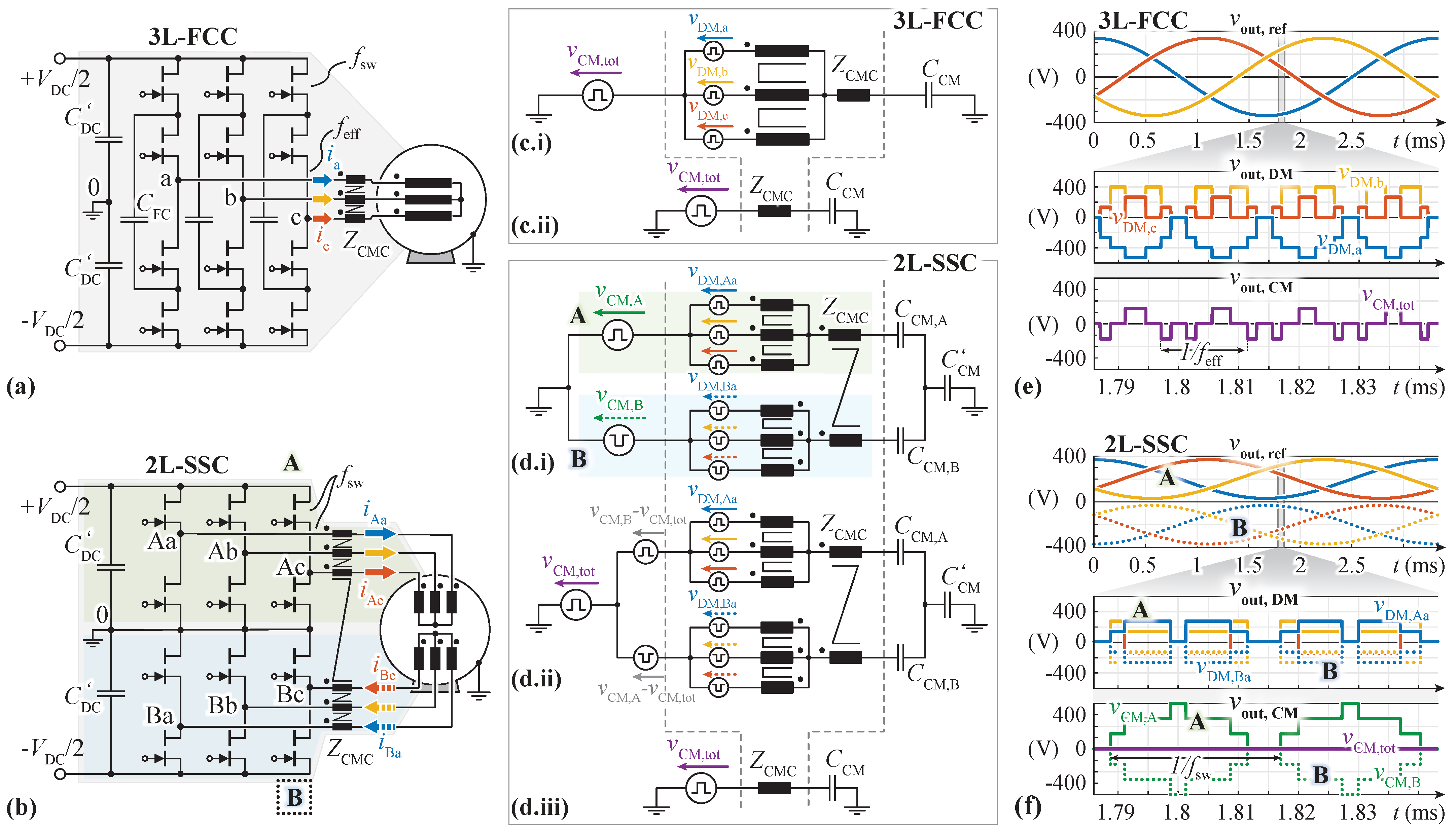
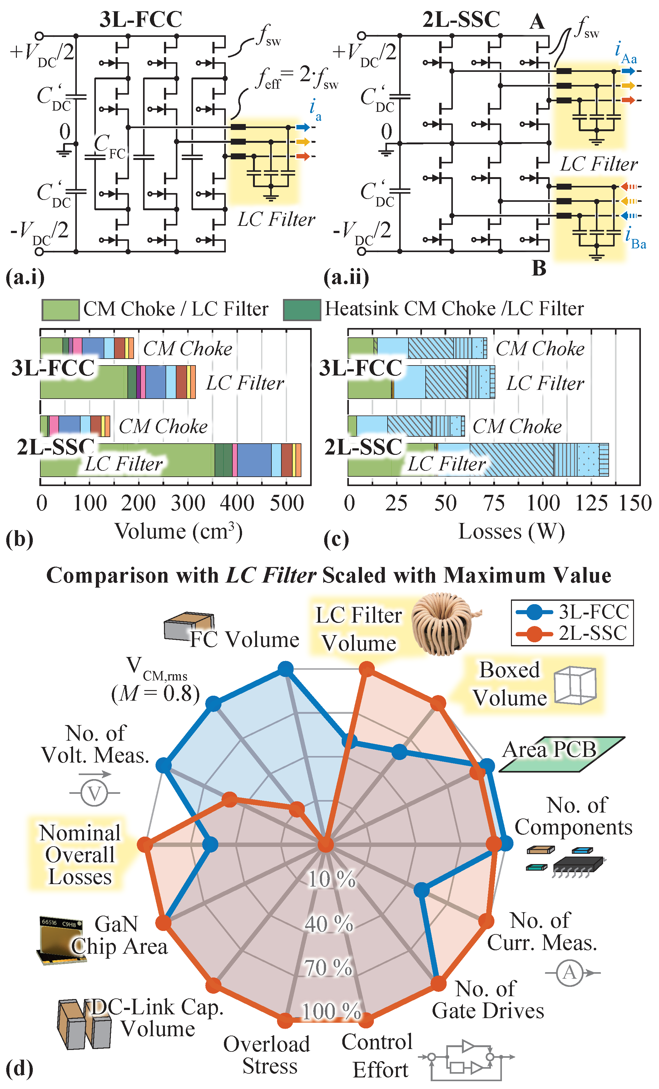
This section provides a brief overview of the operating principles of the 3L-FCC and the 2L-SSC, including the possibility of achieving mutual CM cancellation with the latter for a symmetric motor design. Subsequently, the resulting CM output voltages generated from both topologies are discussed and analytically compared over a full output voltage/current fundamental period.

2.1. 3L-FCC

The 3L-FCC depicted in Figure 1a utilizes two half-bridge cells per phase (i.e., four switches in total, each required to block only half the total DC-link voltage V dc ) and a Flying Capacitor C FC to provide three output voltage levels. The effective frequency f eff , which is measured at the switch node advantageously is twice the device switching frequency, i.e., f eff = 2 · f sw .
The third output voltage level is generated by including the FC in the output current path. Consequently, within a (device) switching period, the FC is charged and subsequently discharged again with the output current for a maximum duration of one effective switching period [29]. This leads to a certain (peak-to-peak) voltage ripple amplitude of Δ V FC around the nominal DC value of the FC voltage, which is V DC / 2 . During operation, said DC voltage value is ideally maintained by the natural balancing capability when employing Phase-Shifted PWM (PSPWM). However, in reality, natural balancing might not suffice [10,11,12], and, consequently, the active balancing concepts of the FCs [30,31] must be implemented to guarantee reliable performance of the motor drive.
As shown in the equivalent circuit of Figure 1(c.i,c.ii,) the switched three-level output voltages provided to the motor can be separated in a CM ( v CM , tot ) and in three DM components ( v DM , a , v DM , b and v DM , c ). With a focus of this paper on the CM voltage limitation at the motor terminals, the final CM equivalent circuit is depicted in Figure 1(c.ii). Note that the CM impedance of the motor is represented with a CM capacitance C CM only; this is a useful approximation, which will be discussed in Section 3.4. The respective switched CM and DM waveforms are shown in Figure 1e for a small section of the sinusoidal output voltage references v out , ref . Thereby, the CM voltage v CM , tot attains values between ± V DC / 6 = ± 133   V .

2.2. 2L-SSC

The 2L-SSC in Figure 1b consists of two standard three-phase 2L inverters (i.e., hereinafter called inverter A (blue in Figure 1b) and inverter B (green) connected in series at the DC side such that each 2L inverter is supplied with half the total DC-link voltage. Consequently, the same transistor count as in the 3L-FCC results, and the transistor blocking voltages are identical, too. The two inverters drive a dual-winding-set motor with the following two three-phase winding systems: the first three-phase winding is connected to inverter A and the second to inverter B. Both inverters provide the same output phase current levels as the 3L-FCC but at only half of the 3L-FCC’s phase voltages. Thus, in total, the same output power and torque as in the single three-phase winding machine driven by the 3L-FCC results.
A balanced DC-link voltage mid-point (marked with “0” in Figure 1b) is a necessary condition for the successful operation of the 2L-SSC throughout the motoring and generating mode of the PMSM. When employing the common-duty-ratio control [32], i.e., only the output currents of inverter A are actively controlled and inverter B uses the identical switching pattern, the DC-link voltage mid-point is asymptotically stable for initial voltage offsets and DC-link voltage steps. However, in the case of slightly asymmetric machine parameters (i.e., especially minor differences in motor inductance and/or back-EMF of 1–2%) the steady-state DC-link voltage will have an offset, and, even more problematic, the open-loop currents in inverter B will not necessarily generate the expected output torque anymore. Consequently, active balancing is of interest, where the DC-link midpoint voltage can be regulated over a shift in output power from one inverter to the other [18,33,34]. In Field-Oriented Control (FOC), this can be achieved by altering the otherwise identical q-current component references of the two inverters, which will result in slightly different output voltage references. Note, however, due to substantially symmetrical industrial motor designs, the required shift in power, i.e., the variation in the output voltage reference, is expected to be small.
In Figure 1(d.i–d.iii), the corresponding equivalent circuit using the switched output voltages is shown with separated CM and DM contributions. Again, as will be discussed later, the motor CM impedance is capacitive for the frequency range of interest. Thereby, the motor CM capacitances are split into C CM , A , C CM , B (taking into account the direct coupling between the two adjacent stator winding systems) and C CM (taking into account the coupling of these windings via the rotor, and the coupling to the motor housing/earth) [27]. Deriving the total CM voltage from the CM voltages of inverter A ( v CM , A ) and of inverter B ( v CM , B ) yields
v CM , tot ( t ) = v CM , A ( t ) + v CM , B ( t ) 2 .
The CM equivalent circuit in Figure 1(d.iii) follows directly, with the total motor CM capacitance C CM representing the series connection of ( C CM , A + C CM , B ) and C CM .
Consequently, in order to achieve mutual CM cancellation, i.e., v CM , tot ( t ) = 0 , inverter A and inverter B must be driven by complementary output voltage references v out , ref , which result in complementary switching patterns that lead to v CM , A ( t ) = v CM , B ( t ) , as shown Figure 1f. As a side effect, the phase currents of inverter B flow in the opposite direction compared to those of inverter A. This requires that one of the motor’s winding systems is connected with a reversed winding direction (indicated by the dots representing the respective winding start in the schematics of Figure 1b) such that both windings generate torque components in the same direction.

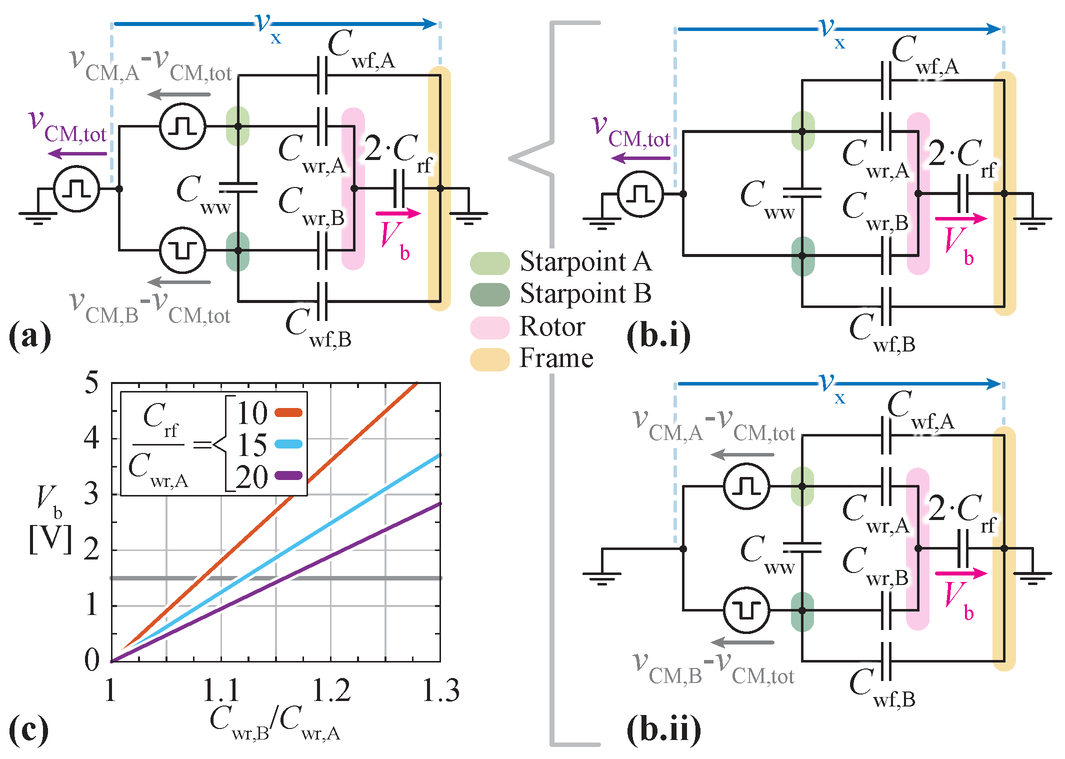
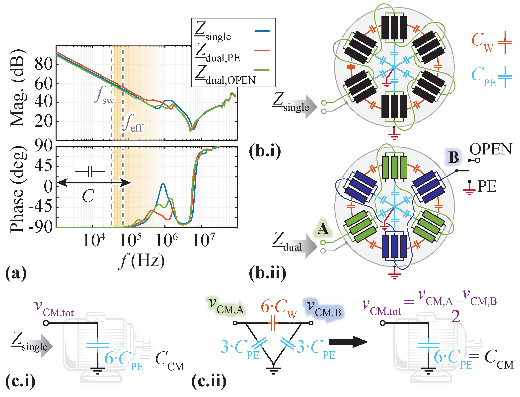
2.3. Quantitative Comparison of Resulting CM Voltages

In order to put the generated output CM voltages of the 3L-FCC and the 2L-SSC quantitatively into perspective, the total rms value V CM , rms can be computed over a fundamental output voltage period. For comparison, a state-of-the-art six-switch 2L inverter with the conventional Space Vector PWM (SVPWM) leads to a total CM rms voltage [35] of
V CM , rms , 2 L = ( 3 · π 4 · 3 · M ) · V DC 2 12 · π ,
whereas equivalent considerations for the 3L-FCC with a conventional PSPWM result in
V CM , rms , 3 L = ( 2 3 ) · M · V DC 2 6 · π ;
both rms voltages vary with the modulation index M (i.e., M = V out / ( V DC / 2 ) with V out as the phase output voltage amplitude referenced to the DC-midpoint (marked with “0” in Figure 1a). Thanks to the higher number of output voltage levels, a remarkable reduction in V CM , rms of the 3L-FCC compared to a 2L inverter is achieved, which is visualized in Figure 3a when operated with a DC-link voltage of V DC = 800   V according to Table 1. Especially for low M, the third output voltage level of the 3L-FCC enables a massive reduction in V CM , rms .
In the 2L-SSC, theoretically ideal CM voltage cancellation is possible, as shown in Figure 1f. It is important to note that the introduction of dead times t dead (interlock delay times needed between turning off the first of the half bridge’s transistors and turning on the complementary transistor of the bridge leg) has (ideally) no impact on the CM voltage cancellation capability of the 2L-SSC. This is exemplarily shown in Figure 2b for the current directions indicated in Figure 2a as follows: the output currents in both inverters A and B are (ideally) identical in amplitude but 180° out of phase (cf. i Aa and i Ba in Figure 2a). Combined with the inverted switching pattern of inverter A and B required for CM cancellation, this leads to simultaneous “soft” switching transitions (the switch-node voltage changes at the turn-off of a transistor, cf. at time t 1 in Figure 2b) and simultaneous “hard” switching transitions (the switch-node voltage changes only at the turn-on of a transistor, cf. at time t 2 + t dead in Figure 2b) of inverter A and B. Hence, the insertion of a dead time t dead between turn-off, e.g., T LS , Aa and T HS , Ba at time t 2 , and turn-on of the complementary transistor of the respective bridge leg, i.e., T TS , Aa and T LS , Ba at time t 2 + t dead , shifts the switch-node voltage transitions of inverter A and inverter B identically, such that the ideal CM voltage cancellation is maintained.
However, a certain delay t d of the gate signals of inverter B compared to inverter A (e.g., as a consequence of differences in Printed Circuit Board (PCB) layout and/or component propagation delays) will result in a non-zero v CM , tot as depicted in Figure 2c: v CM , tot contains a voltage spike of duration t d and amplitude ± V DC / 12 at every misaligned switching transition of inverter A and inverter B, which leads to a total CM rms voltage of
V CM , rms , tot ( t d ) = t d · f sw · V DC 2 24 .
Alternatively, non-ideal CM cancellation occurs when the DC-link needs to be balanced by the unequal distribution of the output power between inverter A and inverter B. Thereby, e.g., the output current of inverter A is slightly increased and the output current of inverter B is slightly decreased, which, as a first approximation, requires a marginal increase/decrease in the respective output voltage references by the correction factor m f . With the adjusted modulation indices of M A = M · ( 1 + m f / 2 ) and M B = M · ( 1 m f / 2 ) for inverter A and B, respectively, a total CM rms voltage of
V CM , rms , tot ( m f ) = M · | m f | · V DC 2 48 · π
results. Note that the modulation index M in case of the 2L-SSC is defined as M = V out / ( ( V DC / 2 ) / 2 ) with V out as the phase output voltage amplitude referenced to the virtual midpoint of the DC-link input voltage of inverter A (resp. B). However, despite these two non-ideal CM cancellation scenarios, the resulting CM voltage of the 2L-SSC is considerably lower than for the 3L-FCC. This is clearly visible in Figure 3a for a large delay of t d = 100   n s or a large balancing factor of m f = 0.1 . Figure 3(b.i,b.ii) highlights how a the total CM rms voltage of the 2L-SSC further reduces with shorter delays t d or lower balancing correction factor m f , i.e., approaching ideal cancellation.

3. Design Considering Short-Term Overload Capability

In order to compare the two topologies in terms of achievable power densities and efficiencies, both the 3L-FCC and the 2L-SSC are designed for the same specifications given in Table 1, i.e., the identical DC-link voltage, total output power, short-term overload capability, and accepted peak CM voltage v x , max at the motor terminals. Note that the short-term overload requirement (i.e., three times nominal current during 3 s ) is targeted for a broad range of inverter output frequencies f out , i.e., from motor standstill ( f out = 0 Hz ) to ( f out = f out , max = 300 Hz ). The important design aspects of semiconductors, capacitors, and CM choke are summarized in the following, and the key stress metrics for the main components are compiled in Table 2.

3.1. Semiconductors

The required blocking capabilities V ds , nom = 400   V of the semiconductors in the 3L-FCC and 2L-SSC are identical and equal half the total DC-link voltage. Furthermore, given the same output power, both topologies result in the same rms current stress for the semiconductors.
Assuming identical device switching frequencies, f sw , the 3L-FCC’s switch-node voltage shows an effective switching frequency of f eff = 2 · f sw , i.e., twice that of the 2L-SSC’s switch-node voltages (cf. Figure 4). Consequently, the device switching frequency of the 3L-FCC could be reduced to half the value of the 2L-SSC for the same effective switching frequency at the switch node. This, however, increases the required HF DC-link capacitor volume, the FC volume, and the CM choke volume; all discussed in more detail later. Hence, identical device switching frequencies are maintained for both the topologies in this paper, and the increased effective switching frequency f eff of the 3L-FCC is used to minimize the FC and the CM choke volumes.
With identical device switching frequencies, equal semiconductor losses (conduction plus switching losses) occur in both converters, especially as for typical DM motor phase inductances in the order of several hundred μ H to several m H , the difference in the motor current ripple is negligible for the considered switching frequency. This leads to an identical choice of semiconductors for the two topologies, i.e., the same semiconductor count and total chip area.
In order to account for voltage overshoots during switching transitions, as well as for Flying Capacitor and/or the DC-link voltage ripple, 650 V power transistors are used. For this voltage range Wide-Bandgap (WBG) devices (e.g., SiC or GaN technology) offer superior on-state and switching characteristics, which allow high switching frequencies at low semiconductor losses. The impact of the overload capability on the selection of semiconductors available on the market has been discussed in detail in [5]. The large currents during the overload operation lead to dominating conduction losses, and thus, only semiconductors with low R dson values (i.e., large die areas) and good cooling performance (low R th and large cooling pads) are feasible. This leads to an implementation of a single switch with two parallel top-cooled 650 V GaN HEMTs (GS66516-T, 25 m Ω , [36]) for both, the 3L-FCC and the 2L-SSC. The detailed switching loss data of these devices are also provided in [5].

3.2. Flying Capacitors

The 3L-FCC has one FC per phase with a bias voltage of half the DC-link voltage, while there are no FCs in the 2L-SSC. As discussed in Section 2.1, the charging and discharging of the FCs with the respective bridge leg output phase current leads to a minimum required capacitance of
C FC = i out f eff · Δ V FC , max
for the worst-caste duty cycle of d = 0.5 [29] and a specified peak-to-peak FC voltage ripple Δ V FC , max in Table 1. Thereby, the short-term overload capability of three times the nominal current determines C FC since then i out = I out , OL [5]. Note that the Flying Capacitor volume, as well as the HF DC-link volume (for both the 3L-FCC and the 2L-SSC), could be reduced by increasing the switching frequency during overload as performed in [5]. However, it leads to an increased implementation effort and is not further considered here.
Besides the voltage ripple criterion, a minimum number of paralleled capacitors is required in order to not exceed the maximum rated temperature of the chosen capacitors due to the Equivalent Series Resistance (ESR) losses. Especially during overload operation, the worst-case rms current (for d = 0.5 ) of I FC , rms = i out = I out , OL needs to be accounted for.
Finally, for implementation, 450 V X6S ceramic capacitors (C5750X6S2W225K250KA, 2.2   μ F , [37]) are chosen because of their high capacitance density per volume (including the capacitance derating with applied bias voltage). It results in a minimum of 24 paralleled ceramic capacitors for the FC stage per phase.

3.3. High Frequency (HF) DC-Link Capacitors

The DC-link capacitors are designed to restrict the HF DC-link voltage ripple Δ V DC , max to a maximum peak-to-peak value, as specified in Table 1.
  • 3L-FCC: Only the switching states of the two complementary semiconductors next to the DC-link capacitor (cf. T 1 and T 1 ¯ in Figure 4a) define the HF component of the DC-link current regardless of the switching state of the other semiconductors (cf. T 2 and T 2 ¯  Figure 4a). Consequently, the HF DC-link voltage ripple (contrary to the FC voltage ripple) is directly related to the device switching frequency f sw (and not the effective switching frequency f eff at the switch nodes). Hence, as seen from the DC-link, the inverter behaves like a standard three-phase 2L inverter. For the design, in a first-step approximation, only a single phase leg is considered. It can then be assumed that the full HF current is covered by the HF DC-link capacitors, which leads to a required capacitance value of
    C = 1 4 · i out f sw · Δ v pp
    for a duty cycle of d = 0.5 with a desired peak-to-peak voltage ripple of Δ v pp = Δ V DC , max [38]. Similar to the FCs, an overload operation with i out = I out , OL determines the required capacitance.
    Two series connected rows of, in total, 176 X6S ceramic capacitors, each rated for 450 V (C5750X6S2W225K250KA, 2.2   μ F , [37]), can be used for the implementation (i.e., every row with a value of C DC = 2 · C DC to account for the series connection). This large number of discrete capacitors for the DC-link realization can be impractical for industrial applications. Alternatives with fewer discrete devices (e.g., pre-assembled CeraLink capacitor units [39] or even film capacitors) would increase the converter volume, but simplify manufacturing and possibly contribute to increased reliability (i.e., fewer discrete devices and soldering connections that can potentially break). Note that to comply with the thermal limitation of the capacitors, the total rms current of I DC , rms = I out , OL / 2 , based on a 2L motor drive derived in [40], must be taken into account. According to Figure 1a, the DC-midpoint (marked with “0”) can be used as a ground reference, but remains completely unloaded.
  • 2L-SSC: The 2L-SSC consists of two stacked three-phase 2L-inverters, each with their own HF DC-link capacitor C DC at half the DC-link voltage. Due to the inverted switching patterns and phase currents, the currents drawn from their respective HF DC-link capacitors C DC are identical for both inverters A and B. Thus, the HF voltage ripple limitation can be applied to inverter A and inverter B independently. Using the same single-phase approximation introduced above for the 3L-FCC, the required capacitance per stacked inverter can be approximated with (7) and Δ v pp = Δ V DC , max / 2 (since the respective voltage ripples will be summed up directly due to the identical DC-link currents of inverter A and inverter B). All in all, the series connection of the two C DC results in an identical total DC-link capacitance value C DC as for the 3L-FCC. Hence, it can be built in the same way and for identical rms current loading.
Table 2. Worst-case design parameters considering short-term standstill overload operation (i.e., f out = 0 Hz ) with three times nominal output current for 3 s.
3L-FCC2L-SSC
Inverter Output
Δ V step V DC / 2
f eff 2 · f sw f sw
Semiconductors
V ds , nom V DC / 2
I rms , max I out , OL / 2 (*)
DC-link Cap.
V bias V DC
Δ V DC , max I out , OL / ( 4 · C DC · f sw ) [38]
I rms , max I out , OL / 2 [40]
Flying Cap.
V bias V DC / 2 -
Δ V FC , max I out , OL / ( C FC · f eff ) [29]-
I rms , max I out , OL [29]-
* During standstill overload, no back-EMF occurs and, hence, a low-phase output voltage with approximately 0.5 duty cycles is required. In the worst-case scenario, one phase carries the full overload current for 3 s, i.e., I out , OL = 45 A . Thereby, the current flows 50% of the time in the high-side semiconductors and 50% in the low-side semiconductors, leading to a factor of 1 / 2 in the rms current.

3.4. Exemplary CM Choke Designs

The goal of the proposed CM choke designs is to reduce the CM voltages at the motor to a maximum value of v x , max specified in Table 1, such that the destructive edm of the motor bearings is mitigated. In the case at hand, a configurable multi-winding PMSM (designed for an 800 V DC-link with similar rated power as in Table 1 and six configurable three-phase winding sets; shown briefly in [41]) is considered for the 3L-FCC and 2L-SSC design, as it can be configured with either a single or with two winding systems.

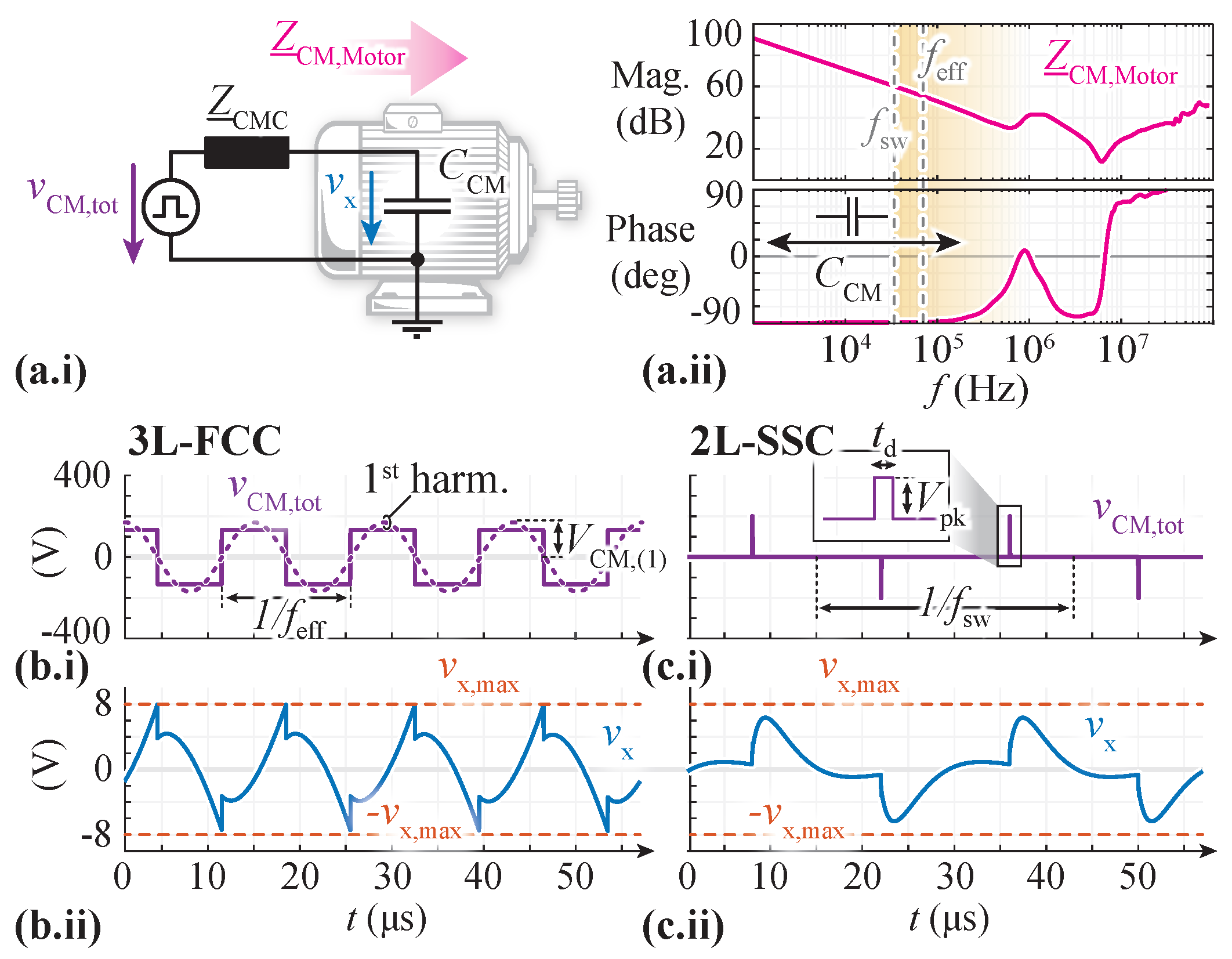
3.4.1. Derivation of the CM Model

In Figure 5(a.i), the equivalent CM circuit of the motor (i.e., represented by a single CM capacitance C CM ) is shown, together with the CM choke (impedance Z ̲ CMC ) to be designed. The CM circuit of the motor is derived from the impedance measured from the configurable multi-winding PMSM presented in Figure 5(a.ii), where the machine behaves purely capacitive up to several multiples of the specified 35 k Hz device switching frequency and, consequently, can be modeled for this range with C CM = 4.4   n F . As shown in the circuit derivation of Figure 1(c.i,c.ii,d.i–d.iii), the resulting CM model of Figure 5(a.i) is valid for both, the 3L-FCC and the 2L-SSC, given that the same symmetric motor is used with altered winding connections. In the Appendix B, this is underlined by the additional impedance measurements performed on the configurable multi-winding-set PMSM for single and dual-winding-set configuration.
The impedance of a practical CM choke Z ̲ CMC can be typically represented by the model depicted in Figure 6b [42]. When neglecting the parasitic capacitance C p of the windings, as well as the relatively small winding losses R w ( f ) , the choke impedance can be calculated as
Z ̲ CMC , calc ( f ) = i · 2 π f · L CMC ( f ) + R CMC ( f ) ,
including a frequency-dependent inductance,
L CMC ( f ) = A L · N L 2 · μ ( f ) | μ ̲ ( f = 0 Hz ) | ,
and a frequency-dependent resistor modeling the core losses,
R CMC ( f ) = A L · N L 2 · 2 π f · μ ( f ) | μ ̲ ( f = 0 Hz ) | ,
where N L is the number of turns, A L the initial inductance per turn squared (i.e., for f close to 0 Hz ), and μ ̲ ( f ) = μ ( f ) + μ ( f ) · i the complex (relative) permeability of the core material provided in datasheets (with i as the imaginary unit).

3.4.2. Worst-Case CM Voltage Design Criteria

For both topologies, the generated CM voltage pattern v CM , tot varies over an output period. However, the charging/discharging (which needs to be limited to prevent edm) of the motor’s CM capacitance, C CM , takes place within a switching period/effective switching period. This means that the local worst-case CM voltage pattern is relevant for the CM choke design.
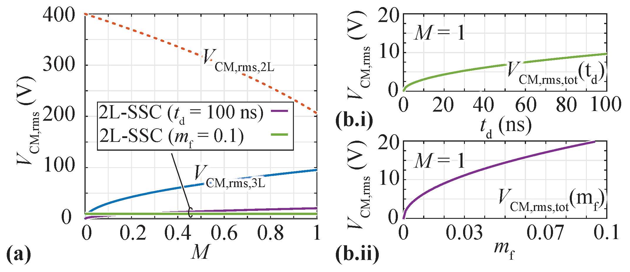
  • 3L-FCC: In conventional PSPWM, the worst-case v CM , tot occurs for sinusoidal modulation (i.e., with a modulation limit of M = 1 , without a third harmonic CM voltage injection) when one of the phases passes through the peak output voltage with, e.g., phase leg duty cycles of d a = 1 , d b = d c = 0.25 . The resulting simulated CM voltage is shown in Figure 5(b.i), together with its dominating first harmonic component at f eff with a maximum amplitude of V CM , ( 1 ) = ( π / 4 ) · V DC / 6 = ( π / 4 ) = 170   V . In order to comply with the given design specifications, the excitation of the first harmonic has to be attenuated to a maximum peak amplitude of v x , max over C CM (red dashed line in Figure 5(b.ii)). All higher-order harmonics are not explicitly addressed with this approach, as they are, first, of lower amplitude in the first place, and, second, attenuated ideally substantially stronger than the first harmonic (characteristic of a low-pass filter formed by the motor CM capacitance C CM and the CM choke impedance Z ̲ CMC ). Consequently, a CM choke design with an impedance Z ̲ CM satisfying
    v x , max V CM , ( 1 ) = 1 | i · 2 π f eff · C CM · Z ̲ CMC + 1 |
    is required for the 3L-FCC. For the design process Z ̲ CMC can be modeled with (8) as Z ̲ CMC , calc ( f eff ) .
    As a side remark: Note that the dead time t dead (usually in the range of several 10 s of ns) has a negligible influence on the worst-case CM voltage of the 3L-FCC for the given switching frequency and the resulting effective frequency at the switch-node ( T eff = 1 / f eff = 14.3   μ s ).
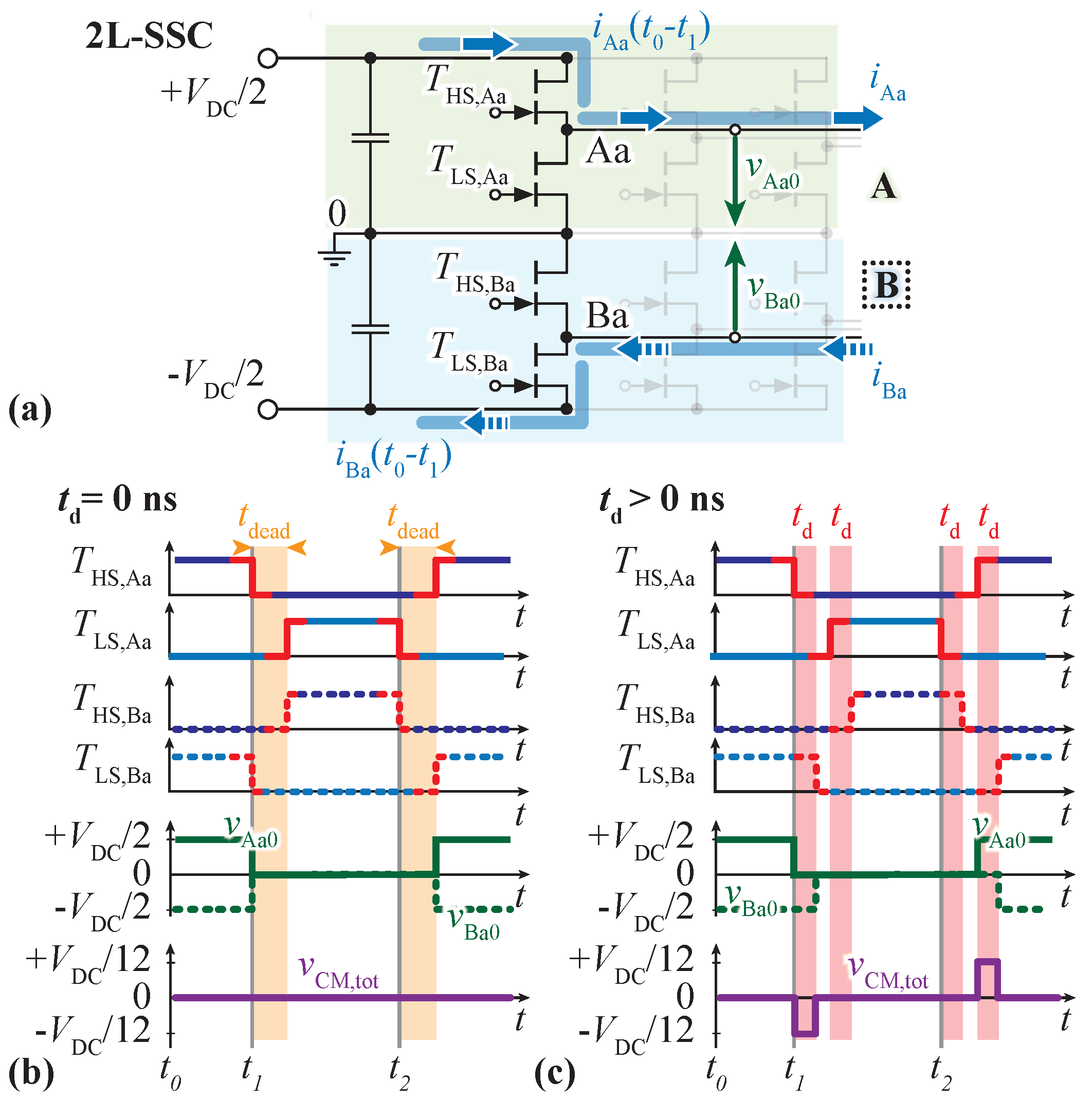
  • 2L-SSC: As discussed in Section 2.2, a significant reduction in the total CM voltage can be achieved thanks to CM cancellation. Thereby, if the two stacked inverters do not switch simultaneously (cf. Figure 2c), only small CM voltage spikes remain, which is, e.g., the case for a delay t d between the switching transitions of inverter A and B as a result of propagation delay mismatches and/or active DC-link balancing actions with correction factor m f . As every single one of these voltage spikes charges the motor CM capacitance C CM , the CM choke has to be designed to limit the increase in voltage during those CM spikes. Thereby, the largest voltage-time area (i.e., the longest spike duration with the highest spike amplitude) defines the worst-case, and thus, the required choke impedance Z ̲ CMC .
    In the case at hand, a delay of the corresponding switching actions in the 2L-SSC between inverter A and inverter B of t d = 100   n s is assumed. This is a very conservative upper limit, given that typical propagation delay (mismatches) are in the order of a few 10 ns if high-quality ICs and PCB layouts are used (e.g., in the case of the hardware components in Table 3, the gate driver (1EDN7511B [43]) and the signal isolator (ADuM120N [44]) are both specified with a propagation delay variation of approximately 10 n s in their respective datasheets). However, choosing a very conservative value of t d of 100   n s also accounts for CM voltage spikes caused by potential active DC-link balancing (i.e., m f in Section 2.2).
    Then, in general, six voltage spikes of duration t d = 100   n s and of amplitude ± V DC / 12 = ± 66.7   V result per switching period. The largest instantaneous voltage-time area (i.e., the worst-case scenario) occurs for M = 0 (i.e., all bridge legs operate with a duty cycle d = 0.5 ). In this operating point, the six voltage spikes are temporally aligned/superimposed such that only two CM voltage spikes per switching period with amplitudes V pk = ± 3 · V DC / 12 = ± 200   V remain, as depicted in Figure 5(c.i). Note that M = 0 coincides mostly with the motor standstill operation (i.e, no back-EMF hence low/no inverter output voltage amplitude), where the bearings show a resistive instead of capacitive behavior [27]. However, it is a valid worst-case scenario, which accounts for all possible operating points.
    In contrast to the 3L-FCC above, the first harmonic component does not sufficiently characterize the CM voltage spikes. Therefore, the following approach is suggested: only the inductive part of the choke, i.e., L CMC ( f ) , is considered, which is still a significant part of the impedance at f = f sw , reducing the CM model of Figure 5(a.i) to a simple L C (resonant) circuit. During the voltage spike of duration t d , essentially the full spike voltage is applied over the choke (given that v x is small by design), giving rise to a current increase and, hence, an accumulation of stored energy in the CM choke. After the CM voltage spike, this energy is transferred to C CM , leading to a peak voltage amplitude of v x . The subsequently expected characteristic oscillation of an L C resonant circuit is strongly damped in reality thanks to the (so far) neglected R CMC ( f ) , i.e., the peak voltage is expected to be slightly lower and the oscillation is finished before the next voltage spike occurs. Consequently, with this approach, the design criterion of Z ̲ CMC (i.e., L CMC ) is deduced via the energy balance as
    L CMC = 1 C CM · V pk · t d v x 2 .

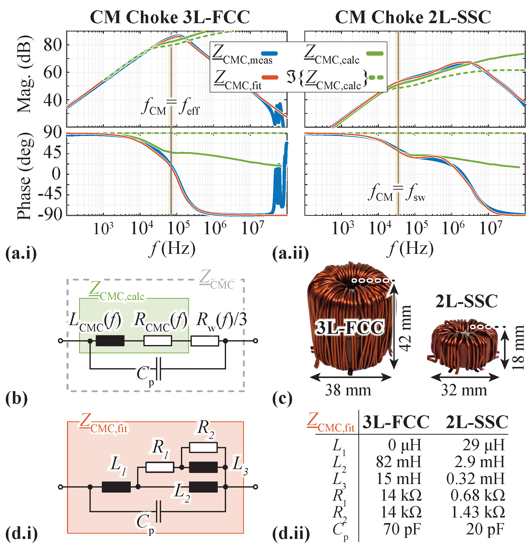
3.4.3. CM Choke Realization

Nanocrystalline materials, such as VITROPERM 500 [45], offer high relative permeability (up to 100,000), high saturation flux density (up to 1.2   T ), and highly resistive core-loss characteristics for frequencies above several 10 s of kilohertz, which facilitates well-damped filter designs. Hence, they are an ideal candidate for the realization of the CM chokes.
In order to meet the requirements for short-term overload capacity, the high phase currents (i.e., 45 A ) must be taken into account when dimensioning the CM choke:
  • Possible core saturation caused by the leakage flux (corresponding to a leakage inductance of several μ H , depending on the inductor design) can be considered already in the design phase [42];
  • The core and winding temperatures should be maintained below 155   C [45] (coinciding with NEMA motor insulation temperature rating Class F [46]). With the majority of the losses originating from the winding, i.e., copper losses, the choke can, e.g., be pressed to the motor housing/inverter baseplate using a Thermal Interface Material (TIM) to achieve sufficient conductive heat transfer. Therefore, a straightforward thermal model consists of a parallel connection of a thermal capacitance (copper winding) and a thermal resistance (cooling path through the copper windings to the side of choke contacting the TIM and then the path through the TIM itself onto the motor housing/inverter baseplate). Starting from the nominal operating point (defined by the thermal resistance only) the choke should not overheat within the 3 s overload operation, despite the strongly increased winding losses during this period.
Together with the design criteria discussed above, commercially available VITROPERM 500 cores and different solid wire diameters were considered (DC winding losses are strongly dominating due to the small output current ripple), and the best-performing design for a semiconductor device switching frequency of 35 k Hz in terms of overall efficiency/power density is selected. Thereby, the three-phase (3L-FCC) and six-phase (2L-SSC) CM chokes shown in Figure 6c result with construction details provided in Table 3. Their measured impedances are shown in Figure 6a, together with the calculated impedance Z ̲ CMC , calc of (8), which was used for the 3L-FCC design (cf. Figure 6b), and the imaginary part of Z ̲ CMC , calc (i.e., 2 π f · L CMC ), which was used for the 2L-SSC design. In order to simulate the resulting voltage v x over the motor CM capacitance C CM by means of circuit simulation software (e.g., PLECS [47]), the measured CM impedances of the choke designs are represented by the fitted L C R -network of Figure 6(d.i,d.ii).
In Figure 5(b.ii,c.ii), the resulting simulated v x are plotted for the respective worst-case v CMC , tot excitations of Figure 5(b.i,c.i). As can be seen for both choke designs, the voltage v x over the motor CM capacitance C CM remains below the limits (dashed red lines), validating the chosen approaches. Nevertheless, the choke design of the 3L-FCC is more critical due to the large parasitic winding capacitance C p , which was not included in the design process. It has a visible influence on the resulting v x as higher frequency voltage components bypass the CM choke, which consequently leads to sharp spikes at the switching transitions.

3.5. Resulting IMD Designs

For the specifications given in Table 1 and the presented CM chokes, the final volume breakdown and required PCB area are shown in Figure 7a and Figure 7b, respectively. Thereby, the dimensions are based on a realized 3L-FCC/7L-FCC hardware presented in [5] (considered PCB areas are recapitulated in Table 3). Note that the heatsink volumes for the semiconductors and the chokes are also accounted for, as discussed in [5]. Thereby, the thickness of the baseplate, where the semiconductor PCBs are mounted, is varied to achieve a maximum temperature of 100 °C below the semiconductors, i.e., an increase of 10 °C compared to the motor housing.
As expected, the semiconductor and gate drive area/volume is identical for both topologies, and the main difference in the overall area/volume originates from the larger CM choke of the 3L-FCC compared to the 2L-SSC (cf. Figure 6c), and the FCs, which are only required in the 3L-FCC. The calculated loss breakdowns at the nominal operating point shown in Figure 7d show identical semiconductor losses for both topologies and, due to the large required die area for overload capability, are dominated by switching losses [5]. However, the total losses of the 2L-SSC are expected to be lower compared to the 3L-FCC, thanks to the small required CM impedance, which results in a CM choke design with a slim core and few winding turns. As can be observed in Figure 7(c.i,c.ii), this results in an expected efficiency of 99.05% for the 3L-FCC and a slightly higher efficiency of 99.2% for the 2L-SSC during nominal operation (cf. red circles). For lower output current amplitudes i out , peak , the efficiencies of the 3L-FCC and 2L-SSC converge, since the winding conduction losses of the choke, which causes the main loss difference, are reduced. On the other hand, during overload, the (short-term) total losses of the 3L-FCC strongly exceed those of the 2L-SSC, due to higher winding losses in its CM choke.
Table 3. Main power components used in the 3L-FCC and 2L-SSC designs.
3L-FCC2L-SSC
Power Transistors
GaN Systems GS66516T ( 650 V , 25 m Ω ),
2 × parallel per position; 27.2 mm2 device chip area [48]
Gate Driver and Gate Drive Insulator
Infineon 1EDN7511B [43]
Analog Devices ADuM121N [44]
CM Choke  Z ̲ CMC
VITROPERM 500F [45]
L2030-W514, 2× stacked;
3× 19 turns of solid copper wire
( A cu = 1.3   m m 2 );
L CMC ( 70   kHz ) = 13   m H ,
R CMC ( 70   kHz ) = 17.3   k Ω
VITROPERM 500F [45]
L2025-W380, 1× stacked;
6x 6 turns of solid copper wire
( A cu = 1.2   m m 2 );
L CMC ( 35   kHz ) = 1.6   m H ,
R CMC ( 70   kHz ) = 0.25   k Ω
DC-Link Capacitors  C DC
Min. 20 μ F , 176 × C5750X6S2W225K250KA (X6S, 2.2   μ F , 450 V ),
i.e., two rows of 88 caps in series
Flying Capacitors C FC
11  μ F , 24 × C5750X6S2W225K250KA
(X6S, 2.2   μ F , 450 V ) per phase
Required PCB Areas according to [5]
Paralleled semiconductors per half-bridge: 9.0 cm2
Gate drive circuit per half-bridge: 9.5 cm2
Overhead per half-bridge: 3.3 cm2
Single voltage/current measurement circuit: 4.5 cm2

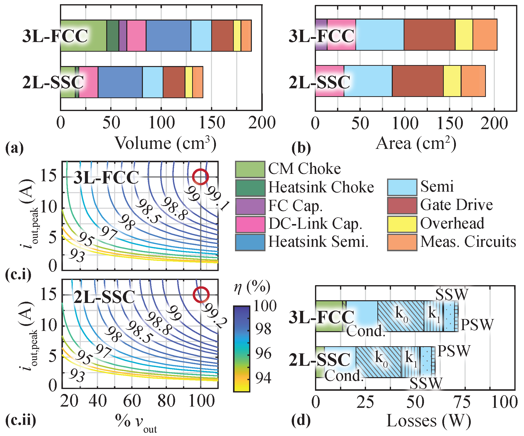
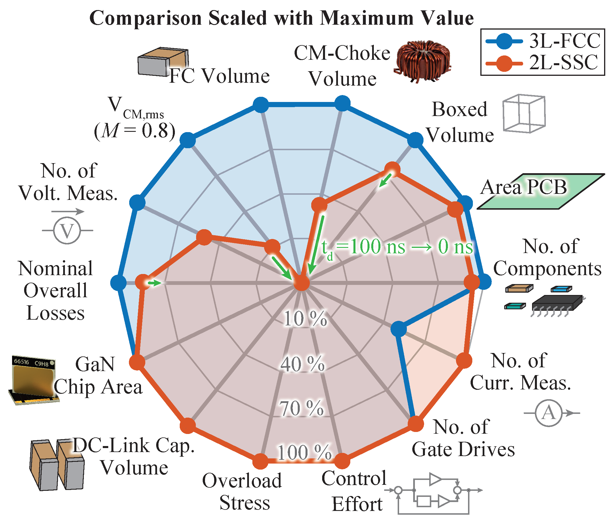
4. Comparative Evaluation

With the expected volumes and efficiencies of both topologies presented in the previous section, an overall comparison of the two possible IMD implementations becomes feasible. Accordingly, the radar plot from Figure 8 provides a visual summary of the main performance characteristics of the 3L-FCC and 2L-SSC equipped with CM chokes for mitigating the EDM bearing currents, which serves as a basis for the following comparison and discussion.

4.1. Mechanical Realization Effort

As mentioned in Section 3, the realization effort of the 3L-FCC and the 2L-SSC is identical in terms of the required switches (and gate drives), as well as regarding the total semiconductor chip area defined by the overload capability. Similarly, the total required (HF) DC-link capacitance, its voltage rating, and rms current capability are the same for the 3L-FCC and 2L-SSC, with the only difference in a mandatory (internal) DC-link midpoint in the case of the 2L-SSC.
Note that despite the identical total semiconductor chip area of the two topologies, the 2L-SSC benefits from a possible standard six-pack semiconductor arrangement, whereas the 3L-FCC requires a more dedicated bridge leg design, which is a clear advantage of the 2L-SSC that is not captured in the Figure 8.
A clearly visible key benefit of the 2L-SSC is the elimination of the FCs, which leads to a reduction in the required PCB area (cf. Figure 7b) and of the number of discrete components placed in the system. Furthermore, thanks to the possibility of CM cancellation and the subsequently improved CM output voltage quality, the CM choke of the 2L-SSC is considerably smaller in volume, even in the case of a non-ideal cancellation with the assumed worst-case misalignment of t d = 100   n s between inverter A and B. Note that the CM choke volume of the 2L-SSC can be minimized even further when a low t d can be guaranteed as indicated with green arrows in Figure 8.
All in all, the elimination of the FC and the considerably smaller CM choke volume lead to a smaller possible system realization (i.e., smaller boxed volume) of the 2L-SSC compared to the 3L-FCC.

4.2. Losses and Overload Capability

The switching and conduction losses in the semiconductors of the 3L-FCC and 2L-SSC are the same based on the chosen identical device switching frequencies (i.e., the increased effective switching frequency of the 3L-FCC is used to minimize its FC and CM choke volume) combined with the negligible phase current ripple in the relatively large motor phase inductances. However, thanks to the required lower CM choke impedance of the 2L-SSC, the CM choke design results in a smaller total winding length (i.e., all six windings together) and the associated winding copper losses are reduced compared to the 3L-FCC despite the slightly smaller solid wire cross-section of the optimal design. This can be seen in the overall loss breakdown presented in Figure 7d.
During the overload operation, an equal stress increase is expected for the key components of both topologies. This characteristic is quantified in [48] (with temperature-critical semiconductors in the forefront) and shows the utilization of the maximum allowed semiconductor junction temperature after a 3 s standstill overload operation with 45 A peak current in one phase. The junction temperature evaluation considers a transient dynamic thermal model with non-ideal heat spreading in the baseplate, on which the PCB with the semiconductors is mounted [5]. Consequently, with identical semiconductor devices and identical overload losses, the same junction temperatures, and hence the same overload stresses, are expected. As a side remark, note that also for the designed chokes a similar temperature increase (remaining below 155 °C) is expected within the 3 s overload. Thereby, the reduced copper mass of the 2L-SSC choke offers less thermal capacitance to buffer the short-term surge of (mainly) winding losses compared to the design of the 3L-FCC. On the other hand, these winding losses are significantly lower in the 2L-SSC and the overall smaller size of the choke allows a better thermal connection to the motor housing for cooling, which finally leads to a similar thermal behavior in the event of overload).

4.3. Measurement Effort

The number of necessary voltage and current measurement circuits represents an adequate quantification of the measurement effort of a three-phase IMD implementation. In the case at hand, both the 3L-FCC and the 2L-SSC require six measurement units in total. Thereby, for the 3L-FCC four voltage measurements, one for the full DC-link and one for each Flying Capacitor are accounted for. Furthermore, at least two output phase current measurements are needed for the operation of a single three-phase machine winding system (in an open-star configuration). Note that advanced Flying Capacitor balancing techniques, as suggested in [31], which rely on the manipulation of the switching pattern based on the current ripple (i.e., omit the direct measurement of the Flying Capacitor voltages), are substantially more complicated, especially when considering the following: (1) the ripple might be small when a large motor inductance defines the ripple instead of a dedicated output filter inductance, and (2) the three-phase currents are coupled in an open-star configured machine without DC-side referenced output filter capacitors, which has also a direct impact on the ripple.
Meanwhile, the 2L-SSC only relies on two voltage measurements (full DC-link voltage and DC-midpoint) but requires four output current measurements for the dual three-phase winding system.

4.4. Control Effort

The measurements are used to actively control the respective energy storage units of the system (i.e., the voltage of capacitors and the currents in the motor phase inductances). Consequently, the number of these energy storage units can be used to describe the control effort featured in Figure 8. In the present case, it is identical for both topologies with five energy storage units each as follows:
For the 3L-FCC, the single three-phase winding PMSM in dq-frame (as used in Field-Oriented Control) accounts for two units to be controlled, i.e., d-current and q-current component, while the actively balanced Flying Capacitor voltages of every phase contribute the remaining three units. Contrary to the 2L-SSC, the DC-link midpoint voltage is not connected and, therefore, only requires passive balancing resistors for the potential leakage current variations among series-connected capacitors as used here, see Figure 1a.
In the 2L-SSC, considering non-idealities, only the DC-link midpoint voltage needs active balancing. However, the dual-winding PMSM features two sets of dq-currents [49], i.e., four units to be controlled.
Yet, when considering control complexity, the 2L-SSC might offer the following certain advantage, which is not represented in Figure 8: the dq-frame-based current controller (despite potential coupling in the dual three-phase winding set machine [18]) is rather standard, while the balancing of the FCs is a lesser-known concept for industrial drive systems. Furthermore, e.g., during start-up, special initialization procedures are required to charge the FCs equally, which is not necessary for the split DC-link voltage of the 2L-SSC. Said split DC-link capacitor of the 2L-SSC could also be more easily equipped with a larger capacitance than what is strictly required for the HF voltage ripple limitation, which facilitates the voltage balancing in the case of the 2L-SSC further.
Overall, balancing a single DC-link midpoint voltage and controlling two three-phase current systems seems less complex than balancing three FC voltages and a single three-phase current system and, consequently, the 2L-SSC has a certain advantage over the 3L-FCC regarding the control aspect.

4.5. Alternate Scenario: Low Motor Phase Inductance

The presented comparison has been conducted under the assumption that the PMSM has a significant motor phase inductance, i.e., the motor current ripple is small. The radar plot of Figure 8 clearly indicates that in this case, an IMD implementation with the 2L-SSC is superior to the 3L-FCC in various aspects. It increases the performance by reducing the total inverter losses and achieves an overall smaller volume. The considerably less bulky CM choke volume facilitates motor integration and allows a more compact and flexible design for various motor shapes.
However, the motor phase inductance might be considerably lower for, e.g., high-speed machines with low turn counts of the stator windings [50]. For identical motor current ripples in the case of the 2L-SSC and the 3L-FCC, the device switching frequency f sw of the 2L-SSC must be doubled compared to the 3L-FCC to achieve the same effective switching frequency f eff at the switch node. If one also takes into account that the phase inductance of the dual-winding motor is likely to be around half that of a single-winding motor for the same power/torque specifications, the device switching frequency required to achieve a similar output current ripple would actually quadruple for the 2L-SSC, and thus increase the expected inverter losses considerably. For such a system, the higher effective switching frequency offered by the 3L-FCC is a clear advantage.

4.6. Alternate Scenario: Full Sine-Wave Output Filter

To date, only a CM filter was targeted to mitigate EDM bearing current damages. However, for the 2L-SSC the presented analysis relies on a symmetric motor design; if symmetry in the mechanical setup is not present, the CM cancellation approach does not completely prevent the buildup of voltages across the bearings despite the CM choke (see Appendix A for a brief discussion). Consequently, in order to mitigate the EDM bearing currents in such cases, or, more generally, to maximize the inverter’s motor-friendliness and, in non-IMD applications, the compatibility with long motor cables, a combined DM and CM output voltage filter, as shown in Figure 9a, i.e., a DC-midpoint referred full sine-wave L C filter stage highlighted in yellow, has to be employed. This full sine-wave filter eliminates HF motor losses and completely protects the motor from the power electronics (e.g., from high dv/dt and CM voltages). This approach has been thoroughly discussed in [5] for the 3L-FCC and is here briefly extended to the 2L-SSC.
The total volume of such an L C filter in an 2L-SSC is inherently doubled compared to the 3L-FCC, even when assuming an identical effective switching frequency at the switch node (i.e., the 2L-SSC requires twice the device switching frequency compared to the 3L-FCC).: Although this leads to identical voltage-time areas over the respective filter inductors in both topologies, the two winding systems of the 2L-SSC require two separate sets of filter inductors, each designed for the same nominal/overload current as for the 3L-FCC. Consequently, a doubling of the filter volume and filter losses results, in addition to the doubling of the switching losses due to the doubled device switching frequency), which is shown in the volume comparison in Figure 9b and the loss comparison in Figure 9c, together with the previously discussed volume/losses of the CM choke design for reference (cf. Figure 7a,d). Note that the output filter capacitors of the 2L-SSC, as shown in Figure 9(a.ii), experience a DC-bias voltage differently from the 3L-FCC in Figure 9(a.i). However, their contribution to the filter volume and losses is marginal compared to the filter inductor and thus not discussed further. The clearly larger volume and the higher losses of the 2L-SSC compared to the 3L-FCC are reflected in the comparative radar plot from Figure 9d, where the axes affected by the L C filter (compared to the CM choke case in Figure 8) are marked in yellow. All in all, the 3L-FCC has a clear advantage over the 2L-SSC if a full sine-wave L C output filter is needed, thanks to its increased effective switching frequency, three-level output voltage characteristic, and compatibility with motors with a single-winding system.
As a side remark: Considering passive dv/dt filters (e.g., dv/dt- L C -filters [51]) also twice the volume and losses result for the 2L-SSC compared to the 3L-FCC due to the need for a motor with two winding systems. However, if active dv/dt filters (e.g., gate-driver based dv/dt limitation [51]) are employed, which act on each transistor individually, both the 3L-FCC and 2L-SSC have the same volume/losses due to the identical number of transistors for identical device switching frequency f sw .

5. Conclusions

This paper presents a comprehensive comparison between a 7.5   k W three-phase Three-Level Flying Capacitor Converter (3L-FCC) and a two-Series-Stacked Two-Level three-phase Converter (2L-SSC), targeting next-generation motor-integrated Variable Speed Drives (VSDs) with high short-term overload capability. Advantageously, the 2L-SSC consists of two standard six-switch three-phase inverters with half the total DC input voltage. Thus, standard techniques and components, such as power modules, are applicable, but a non-standard motor with two three-phase winding systems is needed; however, considering motor-integration, this seems of limited importance as no additional external machine terminals are required. In contrast, the 3L-FCC requires more intricate bridge leg structures with Flying Capacitors (FCs) (additional components) whose voltages must be actively balanced (increased control complexity), but is compatible with standard motors.
Both topologies facilitate realizations with a same power semiconductor effort (count, chip area); specifically, 650 V GaN HEMTs are applicable despite the 800 V DC-link voltage. Furthermore, assuming a sufficiently large motor inductance, there is little benefit from doubling the 2L-SSC’s switching frequency to match the effective switching frequency of the 3L-FCC, f eff = 2 · f sw , and thus both systems show identical semiconductor conduction and switching losses.
To mitigate Electric Discharge Machining (EDM) damages to the motor bearings, the maximum Common Mode (CM) voltage at the motor must be limited, which can, as suggested in this paper, be achieved by employing a CM choke that forms a voltage divider with the CM impedance of the motor itself. The CM voltage generated by the inverter ultimately defines the size and losses of the CM choke, whereby the 2L-SSC offers the possibility of (ideally) mutual canceling of the CM voltages generated by the two stacked three-phase two-level inverters. Even under conservative assumptions regarding the non-ideal alignment of the two inverters’ switching transitions and hence non-ideal CM voltage cancellation, the resulting CM choke features only about 30% of the volume and 30% of the (nominal) losses compared to the CM choke needed for the 3L-FCC (even though the 3L-FCC’s CM choke design benefits from the doubling of the device switching frequency, f eff = 2 · f sw , concerning the formation of the output voltage). For such a scenario, the 2L-SSC is clearly the preferable solution. Future experimental verification should confirm the effectiveness of the CM chokes for EDM mitigation in this context.
On the other hand, in case full sine-wave filtering of the inverter output voltages is desired to maximize motor-friendliness and/or to cope with long motor cables in non-motor-integrated applications, the 3L-FCC benefits from the inherent doubling of the device switching frequency at the switch node, whereas the 2L-SSC suffers from the need for two sets of filter elements (inductors and capacitors) due to the two separate winding systems. Thus, identical voltage quality at the motor implies, for example, twice the semiconductor switching losses and twice the filter volume and losses for the 2L-SSC compared to the 3L-FCC.
Finally, the 2L-SSC’s advantages in terms of realization from standardized building blocks like six-pack modules, and the absence of specialized control considerations like for balancing of FCs, remain interesting and relevant from an industrial perspective.
All in all, this paper provides a basis for choosing future concepts of motor-integrated VSD systems with high short-term overload capability.

Author Contributions

Conceptualization: G.R., J.H., S.M. and J.W.K.; methodology: G.R., J.H., S.M. and J.W.K.; formal analysis: G.R.; investigation: G.R., J.H., S.M. and J.W.K.; supervision: J.H. and J.W.K.; writing: G.R. and J.H.; funding acquisition: J.W.K.; project administration: J.W.K.; resources: J.W.K. All authors have read and agreed to the published version of the manuscript.

Funding

This research received no external funding.

Data Availability Statement

Data are contained within the article.

Conflicts of Interest

The authors declare no conflicts of interest.

Abbreviations

The following abbreviations are used in this manuscript:
3L-FCCThree-Level Flying Capacitor Converter
2L-SSCTwo Series-Stacked Two-Level three-phase Converters
ACAlternating Current
CMCommon Mode
DCDirect Current
DMDifferential Mode
FCFlying Capacitor
FCCFlying Capacitor Converter
EDMElectric Discharge Machining
EMIElectromagnetic Interference
ESREquivalent Series Resistance
FOCField-Oriented Control
GaNGallium Nitride
HEMTHigh Electron Mobility Transistor
HFHigh Frequency
IMDIntegrated Motor Drive
PMSMPermanent Magnet Synchronous Motor
PWMPulse Width Modulation
PSPWMPhase-Shifted PWM
RMSRoot Mean Square
SPBIStacked Polyphase Bridge Inverter
SVPWMSpace Vector PWM
TIMThermal Interface Material
VSDVariable Speed Drive

List of Symbols

The following symbols are used in this manuscript:
SymbolDescriptionUnit
A L Inductance per Turn SquaredH
C CM Motor CM CapacitanceF
C CM Part of the Motor CM CapacitanceF
C CM , A , C CM , A Motor CM Capacitance of Winding-Set A and BF
C DC DC-Link CapacitanceF
C DC Split DC-Link CapacitanceF
C FC Flying Capacitor CapacitanceF
C p Parasitic Winding CapacitanceF
C PE Motor CM Capacitance between a Winding-Set and Earth in the employed 18-Phase PMSMF
C rf Motor Rotor-Frame CapacitanceF
C W Motor Winding-Winding Capacitance (between Winding-Sets in the employed 18-Phase PMSM)F
C wf , A , C wf , B Motor Winding-Frame Capacitance of Winding-Set A and BF
C wr , A , C wr , B Motor Winding-Rotor Capacitance of Winding-Set A and BF
C ww Motor Winding-Winding Capacitance (between Winding-Set A and B)F
dDuty Cycle
d a , d b , d c Phase Duty Cycles
Δ V DC , max Max. Peak-Peak DC-Link Voltage RippleV
Δ V FC Peak-Peak FC Voltage RippleV
Δ V FC , max Max. Peak-Peak FC Voltage RippleV
Δ v pp Peak-Peak Voltage RippleV
fFrequencyHz
f eff Effective FrequencyHz
f out Inverter Output FrequencyHz
f out , max Max. Inverter Output FrequencyHz
f sw Device Switching FrequencyHz
i Aa , i Ba Current of Phase a of Inverter A and BA
i L Inductor CurrentA
i out Phase Output CurrentA
I out , OL Phase Output Current Amplitude during OverloadA
i out , peak Peak Output CurrentA
I rms , max Max. RMS CurrentA
L CMC Inductive Part of CM ChokeH
MModulation Index
m f Balancing Correction Factor
μ ̲ Complex Relative Permeability
N L Number of Winding Turns
P E Protective Earth
P sw Semiconductor Switching LossesW
R CMC Resistive Part of CM Choke Model (i.e., represents the Core Losses) Ω
R dson Semiconductor On-State Resistance Ω
R th Semiconductor Thermal ResistanceK/W
R w CM Choke Winding Resistance Ω
T 1 , T 2 Gate Signals
T eff Effective Periods
t d Time Delay between Switching Signals of Inverter A and Bs
t dead Dead Time between Turn-Off and Complementary Transistor Turn-On of a Bridge Legs
T HS , Aa , T HS , Ba High-Side Semiconductor Gate Signal of Phase a of Inverter A and B
T j , max Max. Semiconductor Junction Temperature°C
v Aa 0 , v Aa 0 Switch Node Voltages of Inverter A and B referenced to “0” (DC-Midpoint)V
V b Voltage over Motor Bearing/over C rf V
V bias Bias VoltageV
V CM , ( 1 ) Amplitude of First Order Harmonic of the CM VoltageV
v CM , A , v CM , A CM Voltages of Inverter A and BV
V CM , rms Total CM RMS Inverter Output VoltageV
v CM , tot Total CM Inverter Output VoltageV
v DM , a , v DM , b , v DM , c DM Phase VoltagesV
V ds , nom Nominal Semiconductor Blocking VoltageV
V out Phase Output Voltage AmplitudeV
v out , ref Reference Output VoltageV
V pk CM Voltage Spike Amplitude of 2L-SSCV
v sw Switched Output VoltageV
v x Peak CM Voltage at the MotorV
v x , max Max. Peak CM Voltage at the MotorV
Z ̲ CMC Complex CM Choke Impedance Ω
Z ̲ CMC , calc Calculated CM Choke Impedance Ω
Z ̲ dual , OPEN Measured CM Impedance of 18-Phase PMSM configured as Dual-Winding-Set Motor with One Winding-Set Unconnected (=OPEN) Ω
Z ̲ dual , PE Measured CM Impedance of 18-Phase PMSM configured as Dual-Winding-Set Motor with One Winding-Set Connected to PE Ω
Z ̲ single Measured CM Impedance of 18-Phase PMSM configured as Single-Winding-Set Motor Ω

Appendix A. Asymmetries in the Motor

The discussed CM cancellation achievable with the 2L-SSC relies on the basic assumption of a symmetric motor design, i.e., two sets of symmetric motor windings and symmetric capacitive couplings to the rotor and frame. However, in reality, mechanical tolerances must be expected, which can lead to asymmetries in the motor. Their influence on the suggested CM cancellation is briefly discussed in the following with a focus on the parasitic motor capacitances.
Figure A1. (a) A more physical equivalent circuit model of the 2L-SSC with a dual-winding motor. (b.i) Separation into v CM , tot contribution and (b.ii) the remaining winding set CM voltages ( v CM , A v CM , tot and v CM , B v CM , tot ). (c) Potentially occurring voltages over bearing V b in the case of asymmetric C wr , A and C wr , A .
Electronics 13 01259 g0a1
A more physical representation of the CM/DM model of the 2L-SSC in Figure 1(d.i–d.iii) (but shown without the CM choke Z CMC ) is given in Figure A1a [27] with separation into the total CM voltage v CM , tot in Figure A1(b.i), and the two remaining winding-set-specific CM voltages (i.e., v cm , A v cm , tot v cm , B and v cm , A v cm , tot v cm , B ; due to the small CM voltage spikes of v cm , tot ) in Figure A1(b.ii). The voltage over the bearing V b can be seen across the rotor-frame capacitance C rf . Note that the bearing capacitance itself is not explicitly drawn here, as it is comparatively small and in parallel to C rf . The other physical parasitic capacitances occurring in a motor are represented by C wr (winding-rotor), C wf (winding-frame), and C ww (winding-winding).
Note that the model of Figure 1(d.i–d.iii) can be derived from the more physical representation in Figure A1a with
C cm , A = C cm , B = C wf + C wr + 2 · C ww
and
C cm = [ 2 · ( C rf · C wf + C rf · C wr + C wf · C wr ) · ( C wf + C wr + 2 · C ww ) ] / ( C wr 2 + 2 · C ww · C wr + 2 · C rf · C ww )
if both motor winding systems are identical, e.g., C wr , A = C wr , B , i.e., for a perfectly symmetric motor.
Looking at the total CM voltage equivalent part of the model in Figure A1(b.i), one can clearly see that the voltage over the bearing V b is zero if v CM , tot is zero (i.e., ideal CM cancellation with no delays t d , etc.). In the case of a delay (i.e., v cm , tot 0 as in Figure 5(c.i)), V b is approximately 1/10th to 1/20th of v x due to the capacitive divider ratio of C rf / C wr 10 20 [27], as mentioned previously. For this purpose, a CM choke Z CMC was designed in this paper to limit v x to a small specified value of v x , max .
Slight asymmetries in the depicted motor capacitances only marginally vary this capacitive voltage divider ratio of v x , and hence, do not notably impact V b originating from v cm , tot 0 .
However, looking at the remaining winding-set-specific CM voltages of Figure A1(b.ii) (i.e., v cm , A v cm , tot and v cm , B v cm , tot ) a difference in, e.g., C wr , A and C wr , B directly results in a voltage V b 0 across the bearing. This also occurs for ideal CM cancellation, where the voltages v cm , A and v cm , B , as shown in Figure 1f, are directly applicable to Figure A1(b.ii) since v cm , tot = 0 . The resulting offset voltage peak value over C rf can be calculated with superposition as
V b = ( 1 n ) · C wr ( 1 n ) · C wr + 2 · C rf · V
where, e.g., C wr , A = C wr and C wr , B = n · C wr with worst-case V = | max ( v CM , A v CM , tot ) | = 400 V (cf. Figure 1f). Note that the designed CM choke Z CMC (which is not drawn in Figure A1(b.ii) has a negligible impact on this resulting V b , as the CM choke is only dimensioned for small CM voltage spikes and not for the dominant switching frequency harmonics from v cm , A v cm , tot v cm , A .
The resulting calculated V b values are plotted for three different capacitive divider ratios of C rf / C wr in Figure A1c. Assuming a lower limit for the EDM bearing current occurrence at V b = 1.5   V [27], an approximately 10% difference between C wr , A and C wr , B is allowed, which has to be considered during the motor design.

Appendix B. Additional Motor Impedance Measurements

The equivalent CM circuit of a configurable multi-winding Permanent Magnet Synchronous Motor (PMSM) is used in Section 3.4 to design the respective CM chokes for the 3L-FCC and 2L-SSC. This Appendix shows the CM impedance measurements performed on the motor in more detail as follows: In Figure A2a Z ̲ single is obtained for the single-winding-set configuration of the PMSM (cf. Figure A2(b.i)). For the dual-winding-set configuration (cf. Figure A2(b.i)) Z ̲ dual , PE and Z ̲ dual , OPEN are measured. Thereby, Z ̲ dual , PE is obtained when the winding-set of inverter B is connected to PE, i.e., the earth connection of the machine housing, and Z ̲ dual , OPEN when the winding-set of inverter B is unconnected (=“OPEN”). Since the measured CM impedances are capacitive for the frequency range of interest, i.e., f sw = 35 k Hz and f eff = 2 · f sw , these three measurements can be used to determine the capacitances C W between the winding-sets (orange in Figure A2(b.i,b.ii), C W = 0.51 n F ) and the capacitances C PE from the winding sets to earth (blue in Figure A2(b.i,b.ii), C PE = 0.74 n F ); note that already two out of the three measurements suffice for this. The resulting CM equivalent circuit of the single-winding system is shown in Figure A2(c.i) with C CM = 6 · C PE = 4.4 n F . From Figure A2(b.ii), the capacitive CM machine model is directly derived for the dual-winding-set configuration in Figure A2(c.ii), which is identical to the CM machine model already derived for the single-winding-set configuration.
Figure A2. (a) Measured motor CM impedances with the single (i.e., Z ̲ single ) and dual-winding-set configuration (i.e., Z ̲ dual ) shown in (b.i) and (b.ii), respectively. Thereby, Z ̲ dual , PE is measured with the winding-set B connected to PE, i.e., the earth connection of the machine housing, and Z ̲ dual , OPEN with winding-set B unconnected (=“OPEN”). (c.i,c.ii) The resulting CM motor-equivalent circuits, which are identical for the single- and dual-winding-set configuration. Consequently, this model is used for the CM choke design procedure in Section 3.4.
Electronics 13 01259 g0a2

References

  1. Jahns, T.M.; Dai, H. The Past, Present, and Future of Power Electronics Integration Technology in Motor Drives. CPSS Trans. Power Electron. Appl. 2017, 2, 197–216. [Google Scholar] [CrossRef]
  2. Sauer, A. The DC-Factory: Energy Efficient. Robust. Forward-Looking, 1st ed.; Carl Hanser Verlag: Munich, Germany, 2021. [Google Scholar]
  3. Teichmann, R.; Bernet, S. A Comparison of Three-Level Converters Versus Two-Level Converters for Low-Voltage Drives, Traction, and Utility Applications. IEEE Trans. Ind. Appl. 2005, 41, 855–865. [Google Scholar] [CrossRef]
  4. Cittanti, D.; Guacci, M.; Mirić, S.; Bojoi, R.; Kolar, J.W. Comparative Evaluation of 800V DC-Link Three-Phase Two/Three-Level SiC Inverter Concepts for Next-Generation Variable Speed Drives. In Proceedings of the 23rd International Conference on Electrical Machines and Systems (ICEMS), Hamamatsu, Japan, 24–27 November 2020; pp. 1699–1704. [Google Scholar] [CrossRef]
  5. Rohner, G.; Gfrörer, T.; Niklaus, P.S.; Bortis, D.; Schweizer, M.; Kolar, J.W. Comparative Evaluation of Three-Phase Three-Level GaN and Seven-Level Si Flying Capacitor Inverters for Integrated Motor Drives Considering Overload Operation. IEEE Access 2024, 12, 7356–7371. [Google Scholar] [CrossRef]
  6. Holtz, J. Selbstgeführter Wechselrichter. German Patent DE2339034C2, 1 August 1973. [Google Scholar]
  7. Baker, R.H. Bridge Converter Circuit. U.S. Patent US4270163A, 26 May 1981. [Google Scholar]
  8. Nabae, A.; Takahashi, I.; Akagi, H. A New Neutral-Point-Clamped PWM Inverter. IEEE Trans. Ind. Appl. 1981, 17, 518–523. [Google Scholar] [CrossRef]
  9. Brown, M. SIEMENS Standard Drives Application Handbook. 1997. Available online: https://cache.industry.siemens.com/dl/files/430/1160430/att_36835/v1/applications_e.pdf (accessed on 5 June 2022).
  10. Ye, Z.; Lei, Y.; Liao, Z.; Pilawa-Podgurski, R.C.N. Investigation of Capacitor Voltage Balancing in Practical Implementations of Flying Capacitor Multilevel Converters. IEEE Trans. Power Electron. 2022, 37, 2921–2935. [Google Scholar] [CrossRef]
  11. Iyer, R.K.; Petric, I.Z.; Bayliss, R.S.; Brooks, N.C.; Pilawa-Podgurski, R.C.N. A High-Bandwidth Parallel Active Balancing Controller for Current-Controlled Flying Capacitor Multilevel Converters. In Proceedings of the IEEE Applied Power Electronics Conference and Exposition (APEC), Orlando, FL, USA, 19–23 March 2023; pp. 775–781. [Google Scholar] [CrossRef]
  12. Papamanolis, P.; Neumayr, D.; Kolar, J.W. Behavior of the Flying Capacitor Converter under Critical Operating Conditions. In Proceedings of the 26th International Symposium on Industrial Electronics (ISIE), Edinburgh, UK, 19–21 June 2017; pp. 628–635. [Google Scholar] [CrossRef]
  13. Norrga, S.; Jin, L.; Wallmark, O.; Mayer, A.; Ilves, K. A Novel Inverter Topology for Compact EV and HEV Drive Systems. In Proceedings of the 39th Annual Conference of the IEEE Industrial Electronics Society (IECON), Vienna, Austria, 10–13 November 2013; pp. 6590–6595. [Google Scholar] [CrossRef]
  14. Deplazes, R. Neue Transformatorlose Schaltungstopologie für Traktionsantriebe auf der Basis von 3-Stern-Asynchronmaschinen. Ph.D. Thesis, ETH Zurich, Zurich, Switzerland, 1999. (In German) [Google Scholar] [CrossRef]
  15. Han, Y. Design, Modeling, and Control of Multilevel Converter Motor Drive with Modular Design and Split Winding Machine. In Proceedings of the 15th IEEE Workshop on Control and Modeling for Power Electronics (COMPEL), Santander, Spain, 22–25 June 2014. [Google Scholar] [CrossRef]
  16. Nikouie, M.; Zhang, H.; Wallmark, O.; Nee, H.P. A Highly Integrated Electric Drive System for Tomorrow’s EVs and HEVs. In Proceedings of the IEEE Southern Power Electronics Conference (SPEC), Puerto Varas, Chile, 4–7 December 2017. [Google Scholar] [CrossRef]
  17. Pan, Z.; Shrestha, G.; Schweizer, M.; Leppanen, V.M. Cell Voltage Balancing of a Series-Connected Multiphase BLDC Motor Drive. In Proceedings of the International Conference on Electrical Machines (ICEM), Lausanne, Switzerland, 4–7 September 2016; pp. 969–974. [Google Scholar] [CrossRef]
  18. Sierra-Gonzalez, A.; Pescetto, P.; Alvarez-Gonzalez, F.; Heriz, B.; Trancho, E.; Lacher, H.; Ibarra, E.; Pellegrino, G. Full-Speed Range Control of a Symmetrical Six-Phase Automotive IPMSM Drive With a Cascaded DC-Link Configuration. IEEE Trans. Ind. Appl. 2023, 59, 3413–3424. [Google Scholar] [CrossRef]
  19. Bringezu, T.; Biela, J. Comparison of Optimized Motor-Inverter Systems Using a Stacked Polyphase Bridge Converter Combined with a 3-, 6-, 9-, or 12-Phase PMSM. In Proceedings of the European Conference on Power Electronics and Applications (EPE’20 ECCE Europe), Lyon, France, 7–11 September 2020. [Google Scholar] [CrossRef]
  20. Wang, J.; Li, Y.; Han, Y. Integrated Modular Motor Drive Design with GaN Power FETs. IEEE Trans. Ind. Appl. 2015, 51, 3198–3207. [Google Scholar] [CrossRef]
  21. Von Jauanne, A.; Zhang, H. A Dual-Bridge Inverter Approach to Eliminating Common-Mode Voltages and Bearing and Leakage Currents. IEEE Trans. Power Electron. 1999, 14, 43–48. [Google Scholar] [CrossRef]
  22. Han, D.; Lee, W.; Li, S.; Sarlioglu, B. New Method for Common Mode Voltage Cancellation in Motor Drives: Concept, Realization, and Asymmetry Influence. IEEE Trans. Power Electron. 2018, 33, 1188–1201. [Google Scholar] [CrossRef]
  23. Lee, K.; Benson, M.; Dong, X.; Moon, J.; Lee, W. Common-Mode EMI Noise Analysis of Neutral-Point-Less (NPL) Multilevel X-type Inverter. In Proceedings of the Applied Power Electronics Conference and Exposition (APEC), Long Beach, CA, USA, 25–29 February 2024. [Google Scholar]
  24. Skibinski, G.; Kerkman, R.; Schlegel, D. EMI Emissions of Modern PWM AC Drives. IEEE Ind. Appl. Mag. 1999, 5, 47–80. [Google Scholar] [CrossRef]
  25. Evo, M.T.; Alzamora, A.M.; Zaparoli, I.O.; Paula, H.D. Inverter-Induced Bearing Currents: A Thorough Study of the Cause-and-Effect Chains. IEEE Ind. Appl. Mag. 2023, 29, 57–66. [Google Scholar] [CrossRef]
  26. Brown, N.R.; Jahns, T.M.; Lorenz, R.D. Power Converter Design for an Integrated Modular Motor Drive. In Proceedings of the IEEE Industry Applications Annual Meeting, New Orleans, LA, USA, 23–27 September 2007; pp. 1322–1328. [Google Scholar] [CrossRef]
  27. Muetze, A. Bearing Currents in Inverter-Fed AC-Motors. Ph.D. Thesis, Technical University of Darmstadt, Darmstadt, Germany, 2003. [Google Scholar]
  28. Dahl, D.; Sosnowski, D.; Schlegel, D.; Kerkman, R.; Pennings, M. Gear Up Your Bearings. IEEE Ind. Appl. Mag. 2008, 14, 45–53. [Google Scholar] [CrossRef]
  29. Barth, C.B.; Assem, P.; Foulkes, T.; Chung, W.H.; Modeer, T.; Lei, Y.; Pilawa-Podgurski, R.C.N. Design and Control of a GaN-Based, 13-Level, Flying Capacitor Multilevel Inverter. IEEE Trans. Emerg. Sel. Top. Power Electron. 2020, 8, 2179–2191. [Google Scholar] [CrossRef]
  30. Khazraei, M.; Sepahvand, H.; Corzine, K.A.; Ferdowsi, M. Active Capacitor Voltage Balancing in Single-Phase Flying-Capacitor Multilevel Power Converters. IEEE Trans. Ind. Electron. 2012, 59, 769–778. [Google Scholar] [CrossRef]
  31. Stillwell, A.; Candan, E.; Pilawa-Podgurski, R.C.N. Active Voltage Balancing in Flying Capacitor Multi-Level Converters With Valley Current Detection and Constant Effective Duty Cycle Control. IEEE Trans. Power Electron. 2019, 34, 11429–11441. [Google Scholar] [CrossRef]
  32. Mocevic, S.; Aeloiza, E.; Tremelling, D.; Kadachigov, P.; Harnefors, L. DC-Link Stability of Stacked Polyphase Bridges Supplying Multiphase Induction Machine Having Common-Duty-Ratio Control. In Proceedings of the IEEE Energy Conversion Congress and Exposition (ECCE USA), Nashville, TN, USA, 29 October–2 November 2023. [Google Scholar] [CrossRef]
  33. Nikouie, M.; Wallmark, O.; Jin, L.; Harnefors, L.; Nee, H.P. DC-Link Stability Analysis and Controller Design for the Stacked Polyphase Bridges Converter. IEEE Trans. Power Electron. 2017, 32, 1666–1674. [Google Scholar] [CrossRef]
  34. Bringezu, T.; Biela, J. Control of a 9-Phase PMSM with Stacked Polyphase Bridge Converter Including DC Source Impedance. In Proceedings of the 25th European Conference on Power Electronics and Applications (EPE’23 ECCE Europe), Aalborg, Denmark, 4–8 September 2023. [Google Scholar] [CrossRef]
  35. Zhang, D.; Leibl, M.; Mühlethaler, J.; Huber, J.; Kolar, J.W. Modeling and Comparison of CM and DM EMI Pre-Filter Noise Emissions of Three-Phase Voltage and Current DC-Link Converters. IEEE Trans. Power Electron. (TPEL) 2024. under review. [Google Scholar]
  36. GaN Systems. GS66516T Datasheet. 2021. Available online: https://gansystems.com (accessed on 13 April 2023).
  37. TDK. C5750X6S2W225K250KA Datasheet. 2022. Available online: https://product.tdk.com (accessed on 25 September 2023).
  38. Infineon. Input Capacitor (DCLINK) Calculation for Single Phase Motor Bridge—Application Note Z8F80483545. 2023. Available online: https://www.infineon.com/dgdl/Infineon-Input_capacitor_calculation_for_single_motor_bridge-AN-ApplicationNotes-v01_00-EN.pdf?fileId=8ac78c8c8929aa4d0189d5bbe46d21f8 (accessed on 22 June 2023).
  39. TDK Electronics. CeraLink Capacitors. 2024. Available online: https://www.tdk-electronics.tdk.com/en/1054426/products/product-catalog/ceramic-capacitors/ceralink-capacitors (accessed on 22 June 2023).
  40. Kolar, J.W.; Round, S. Analytical Calculation of the RMS Current Stress on the DC-Link Capacitor of Voltage-PWM Converter Systems. IEE Proc.-Electr. Power Appl. 2006, 153, 535. [Google Scholar] [CrossRef]
  41. Kolar, J.W.; Azurza Anderson, J.; Miric, S.; Haider, M.; Guacci, M.; Antivachis, M.; Zulauf, G.; Menzi, D.; Niklaus, P.S.; Minibock, J.; et al. Application of WBG Power Devices in Future 3-Φ Variable Speed Drive Inverter Systems—“How to Handle a Double-Edged Sword”. In Proceedings of the IEEE International Electron Devices Meeting (IEDM), San Francisco, CA, USA, 12–18 December 2020. [Google Scholar] [CrossRef]
  42. Heldwein, M.L.; Dalessandro, L.; Kolar, J.W. The Three-Phase Common-Mode Inductor: Modeling and Design Issues. IEEE Trans. Ind. Electron. 2011, 58, 3264–3274. [Google Scholar] [CrossRef]
  43. Infineon. 1EDN7511B. 2022. Available online: https://www.infineon.com/cms/de/product/power/gate-driver-ics/1edn7511b/ (accessed on 3 February 2024).
  44. Infineon. ADuM121N. 2016. Available online: https://www.analog.com/en/products/adum121n.html (accessed on 3 February 2024).
  45. VACUUMSCHMELZE. EMC Products Based on Nanocrystalline VITROPERM. 2021. Available online: https://staging.vacpim.com/03_Documents/Brochures/EMC%20Products%20based%20on%20Nanocrystalline%20VITROPERM.pdf (accessed on 12 November 2023).
  46. NEMA, N.E.M.A. Motors and Generators MG 1. 2019. Available online: https://www.nema.org/ (accessed on 5 April 2022).
  47. Plexim GmbH. Electrical Engineering Software; Plexim GmbH: Zurich, Switzerland, 2023. [Google Scholar]
  48. Rohner, G.; Gfrörer, T.; Niklaus, P.S.; Huber, J.; Bortis, D.; Schweizer, M.; Kolar, J.W. Hardware-Based Comparative Analysis of Multilevel Inverter Topologies for Integrated Motor Drives Considering Overload Operation. IEEE Open J. Power Electron. 2023, 4, 934–944. [Google Scholar] [CrossRef]
  49. Karttunen, J.; Kallio, S.; Peltoniemi, P.; Silventoinen, P.; Pyrhönen, O. Decoupled Vector Control Scheme for Dual Three-Phase Permanent Magnet Synchronous Machines. IEEE Trans. Ind. Electron. 2014, 61, 2185–2196. [Google Scholar] [CrossRef]
  50. Li, S.; Li, Y.; Choi, W.; Sarlioglu, B. High-Speed Electric Machines: Challenges and Design Considerations. IEEE Trans. Transport. Electrific. 2016, 2, 2–13. [Google Scholar] [CrossRef]
  51. Haider, M.; Niklaus, P.S.; Madlener, M.; Rohner, G.; Kolar, J.W. Comparative Evaluation of Gate Driver and LC-Filter Based dv/dt-Limitation for SiC-Based Motor-Integrated Variable Speed Drive Inverters. IEEE Open J. Power Electron. 2023, 4, 450–462. [Google Scholar] [CrossRef]
Figure 1. (a) Schematic of Three-Level Flying Capacitor Converter (3L-FCC) supplying a three-phase single-winding-set Permanent Magnet Synchronous Motor (PMSM) via a three-phase Common Mode (CM) choke. (b) Schematic of the Stacked Polyphase Bridge Inverter (SPBI) IMD, realized in the form of a two Series-Stacked Two-Level three-phase Converter (2L-SSC), supplying a dual-winding-set PMSM via a six-phase CM choke. In order to achieve CM voltage cancellation, the switching pattern of inverter B is inverse to inverter A, which results in an opposite phase current flow. Identical torque direction in the PMSM is then achieved by reversing the winding direction of the second winding set (note the dots indicating the winding directions). (c.i) Equivalent circuit of the 3L-FCC with separation of the relevant CM and Differential Mode (DM) components, and (c.ii) CM equivalent part only. The PMSM is modeled as a CM capacitance C CM to ground, which represents the motor CM impedance in the frequency range of interest, i.e., around the (effective) switching frequency, see Section 3.4. (d.i) Equivalent circuit of the 2L-SSC with two separate CM and DM sources representing inverters A and B, respectively. The CM voltages are further summarized in (d.ii), which results in the overall CM equivalent circuit in (d.iii). (e) Characteristic CM and DM waveforms of the 3L-FCC. (f) Characteristic CM and DM waveforms of the 2L-SSC: note how the inverse switching patterns of inverters A and B ideally result in a complete cancellation of the CM voltage ( v CM , tot = 0 ).
Electronics 13 01259 g001
Figure 2. (a) 2L-SSC circuit with the amplitude-wise identical but 180° phase-shifted phase currents i Aa and i Ba . The current flowing through the semiconductors is shown for the time interval t 0 to t 1 for the respective switching states defined in (b,c). (b) Inverted on/off signals (e.g., T HS , Aa and inverted T HS , Ba ) required for CM cancellation, and resulting switch-node voltages ( v Aa 0 and v Ba 0 ) and total CM voltage ( v CM , tot ). The dead time t dead does not lead to a misalignment of the switch node voltage transitions, and hence, (ideal) CM cancellation is possible. (c) Switching signals and resulting voltages when a delay t d > 0   n s between inverter A and inverter B occurs, i.e., all on/off signal transitions of inverter B lag inverter A by t d . The resulting misalignment of the switch node voltage transitions leads to a non-zero CM voltage v CM , tot with a CM voltage spike of duration t d at each transition. Note that the same dead time t dead as in (b) is used.
Electronics 13 01259 g002
Figure 3. (a) Analytically derived total CM rms voltages V CM , rms for a fundamental output voltage period over varying modulation index M for V DC = 800   V and f sw = 35   kHz : a state-of-the-art 2L inverter, 3L-FCC, and two curves for 2L-SSCs with non-ideal CM cancellation (one features a delay of inverter B’s gate signals by 100 n s compared to inverter A, and the other requires a balancing correction factor of m f = 0.1 ). (b.i) The sensitivity of V CM , rms of the 2L-SSC with respect to the varying delays of inverter B’s gate signals compared to A for a fixed M. (b.ii) The sensitivity of V CM , rms of the 2L-SSC with respect to a varying balancing correction factor m f for a fixed M.
Electronics 13 01259 g003
Figure 4. (a) Exemplary conduction states for a 3L-FCC phase leg with an output voltage v sw [ V DC / 2 , V DC ] . (b) Respective gate signals (i.e., T 1 and T 2 ) and resulting characteristic output voltage waveform v sw and inductor current i L . Due to the occurring order of the conduction states, the effective switching frequency f eff seen at the output is double the device switching frequency f sw .
Electronics 13 01259 g004
Figure 5. (a.i) Equivalent CM circuit of a PMSM with a purely capacitive motor CM impedance C CM around a switching frequency of f sw = 35   kHz (relevant for the 2L-SSC) and f eff = 2 · 35   kHz (relevant for 3L-FCC). This model is based on the impedance measurement in (a.ii) of the configurable multi-winding PMSM presented briefly in [41]. As shown in Figure 1(c.i,c.ii,d.i–d.iii), this model is valid for both the single-winding-set machine configuration used for the 3L-FCC, as well as the dual-winding-set machine configuration used for the 2L-SSC. (b.i) Worst-case CM voltage v CM , tot for the 3L-FCC, which occurs with sinusoidal modulation for a modulation index of M = 1 when one phase voltage goes through the maximum (i.e., phase-leg duty cycles of, e.g., d a = 1 , d b = d c = 0.25 ). The first harmonic is indicated with a peak amplitude of V CM , ( 1 ) (dashed purple line) as it is relevant for the CM choke design. (b.ii) Simulated voltage v x at the motor C CM when the measured impedance of the 3L-FCC choke design of Figure 6c is used. The maximum values are below the specified limits (dashed red line). (c.i) Worst-case CM voltage v CM , tot for the 2L-SSC, which occurs for a modulation index of M = 0 (i.e., at motor standstill), when all bridge legs switch simultaneously with a duty cycle of d = 0.5 . (c.ii) Simulated voltage v x at C CM when the (measured) impedance of the CM choke realized for the 2L-SSC, shown in Figure 6c, is used.
Electronics 13 01259 g005
Figure 6. Comparison of measured Z ̲ CMC , meas , calculated Z ̲ CMC , calc and fitted Z ̲ CMC , fit impedances of the two CM choke designs for the (a.i) 3L-FCC and (a.ii) 2L-SSC shown in (c). (b) Equivalent model of a CM choke Z ̲ CMC , where the green highlighted part Z ̲ CMC , calc can be calculated with frequency-dependent parameters and is used during the design process. Note that the contribution of the inductive component can be directly seen in (a) in the imaginary part ( Z ̲ CMC , calc ) . (d.i) Equivalent model Z ̲ CMC , fit fitted to the measurement of (a) with parameters given in (d.ii). This model is used for circuit simulations.
Electronics 13 01259 g006
Figure 7. (a) Calculated volume breakdown and (b) PCB area breakdown expected from the two IMD designs. (c.i,c.ii) Calculated efficiencies for nominal and partial load operation at a baseplate temperature of 100 °C for the 3L-FCC and the 2L-SSC, respectively. The red circle highlights the nominal operating point (i.e., i out , peak = 15   A and a phase voltage of v out = 330   V = 100 % at f out = 300 Hz ), where the design target of a minimum efficiency of 99% is defined. The output frequency is linearly reduced with v out (i.e., starting from 300  Hz at 100% v out ), which in a first step corresponds to a practically relevant scenario, where a constant torque at reduced rotational speed is provided. (d) Calculated loss breakdown for the nominal operating point (red circles in (c.i,c.ii)) for the 3L-FCC and 2L-SSC. The semiconductor losses are colored in light blue, with the pattern indicating the distinction between the conduction losses (“Cond.”), the Hard Switching (HSW) (“ k 0 ”, “ k 1 ”) according to P sw = k 0 + k 1 · i sw + k 2 · i sw 2 [5], the Partial-Hard Switching (“PHSW”) losses, and the Soft Switching (“SSW”) losses.
Electronics 13 01259 g007
Figure 8. Radar plot of key characteristics of the 3L-FCC (blue) and the 2L-SSC (red) designed for the same IMD specifications given in Table 1. The 100% values correspond to the maximum value of each category. For a complete IMD implementation, these maximum values are given in the following: CM Choke Volume = 0.046 dm3, Boxed Volume = 0.19 dm3, PCB Area = 2.03 dm2, No. of Components = 1068, No. of Current Measurements = 4, No. of Gate Drives = 12, Control Effort = 5 (quantified as the number of energy storage elements to be controlled), Overload Stress = 95% of Tj,max (quantified as the utilization of the maximum allowed semiconductor junction temperature (i.e., Tj,max = 150 °C) when the peak current is provided during standstill overload), DC-link Capacitor Volume = 0.02 dm3, GaN Chip Area = 653 mm2, Nominal Overall Losses = 71.4 W, No. of Voltage Measurements = 4, VCM,rms = 86.9 V (total rms CM voltage over an output frequency period with M = 0.8) and FC Volume = 0.0078 dm3. The influence on the 2L-SSC design for a reduction in the assumed worst-case misalignment of the switching transitions of inverter A and B from td = 100 ns to td = 0 ns is indicated with green arrows.
Electronics 13 01259 g008
Figure 9. (a.i) Schematics of the 3L-FCC and (a.ii) of the 2L-SSC with full sine-wave L C output filters. (b) Calculated volume breakdown and (c) loss breakdown of the 3L-FCC and 2L-SSC with an L C output filter. For comparison, the previously presented results considering only a CM choke (see Figure 7a) are also shown; the color/pattern code of Figure 7 applies unless otherwise denoted. The device switching frequency of the 2L-SSC with an L C output filter is doubled compared to the 3L-FCC (i.e., f sw = 70   kHz ) to achieve the identical voltage-time area stress of the output filter inductors. In addition to the thus increased switching losses, the two winding systems each require an output filter, which leads to twice the output filter volume and losses for the 2L-SSC. (d) Adapted radar plot of the key characteristics of the 3L-FCC (blue) and the 2L-SSC (red) when a full sine-wave L C output filter is included in the design. The introduction of an L C output filter design mainly alters the yellow highlighted axes, where the maximum values (=100%) are updated as follows: CM Choke Volume = 0.36 dm3, Boxed Volume = 0.53 dm3 and Nominal Overall Losses = 134 W. All other key characteristics remain (nearly) identical.
Electronics 13 01259 g009
Table 1. Specifications of the analyzed Integrated Motor Drive (IMD).
Parameter Value
DC-Link Voltage V DC 800 V
Nominal Output Power P nom 7.5 kW
Nominal Peak Phase Current Amp. I out , nom 15   A
Overload Peak Phase Current Amp. I out , lol 45   A
Overload Duration t OL 3   s
Device Switching Frequency f sw 35 kHz
Max. Inverter Output Frequency f out , max 300 Hz
Motor Case (Ambient) Temperature T case 90%
Min. Nominal Inverter Efficiency η nom , min 99%
Max. Peak CM Volt. at the Motor v x , max 1% of V DC
Max. Peak-Peak DC-link Volt. Ripple Δ V DC , max 1% of V DC
Max. Peak-Peak FC Volt. Ripple Δ V FC , max 10% of V DC / 2
Disclaimer/Publisher’s Note: The statements, opinions and data contained in all publications are solely those of the individual author(s) and contributor(s) and not of MDPI and/or the editor(s). MDPI and/or the editor(s) disclaim responsibility for any injury to people or property resulting from any ideas, methods, instructions or products referred to in the content.

