1. Introduction
With the continuous development of semiconductor technology, the physical limits of MOSFET transistors are unceasingly expanding and many new issues related to reliability are raised. Autonomous driving, biomedical electronics, and advanced integrated circuits all require high reliability to meet the required operating lifetimes. The aging effect degrades the MOSFET transistor and circuit performance. The main factors affecting reliability are negative bias temperature instability (NBTI) [
1,
2] and hot carrier injection (HCI) [
3,
4], which manifest themselves as an increase in absolute threshold voltage (
) and a reduction in the MOSFET transistor current (
), thus degrading circuit performance such as speed, gain, and data stability [
5]. Degradation caused by NBTI is partially recovered after removing the stress voltage [
6,
7], while the degradation caused by HCI is mostly permanent [
8,
9]. By modeling and simulating the degradation, the impact of the aging effects on performance can be evaluated at the design stage to optimize the reliability of the circuit and improve performance, thus greatly improving the reliability of the system and reducing maintenance costs.
As computer-aided design (CAD) technology becomes mature and sophisticated, most integrated circuits are modeled and simulated before fabrication, which contributes to characterizing the circuit reliability. A reliability simulation program calculates the degradation of the MOSFET transistor via the established aging model. Then, the aging effect parameters in the Simulation Program with Integrated Circuit Emphasis (SPICE) model are obtained through the corresponding conversion coefficient, and aging simulations are then performed to predict the circuit lifetime. This paper shows that there is a large error with the conversion coefficient calculated by the traditional method when inversely using the aging simulation parameters to infer the degradation values of MOSFET transistor parameters. Focusing on this problem, a method of calculating the conversion coefficients with high precision is proposed to improve the accuracy of aging simulations. The HCI effect is taken as an example to elaborate the method in detail. We adopted the 0.18 m technology in our experiment because of the significance of the HCI effect in deep sub-micron circuits. This method also applies to the NBTI effect.
2. Lifetime Model and Simulation Parameters
The premise of characterizing circuit aging effects is to establish an accurate accelerated lifetime model that is integrated into circuit simulation software. The degradation of MOSFET transistor parameters is calculated via an aging simulation. Then, the values are converted into the aging parameter in the SPICE model. The degradation of all MOSFET transistors in the circuit can be comprehensively simulated to characterize the influence of the aging effect on circuit performance.
2.1. Accelerated Life Model
Most HCI lifetime models are based on the “lucky electron” model [
10,
11]. Generated interfacial traps (
) have a power-law relationship with the electric field (
) at the drain, drain–source current (
), and stress time (
t), which can be described as follows:
where
W is the channel width,
is the critical energy for electrons to generate interfacial traps,
is the mean free path of the hot electron, and
A is a process dependent constant. According to this model, the MOSFET transistor degradation can be established as follows:
where
,
,
,
,
and
A are fitting parameters via the test data.
is the number of holes or electrons entering the oxide layer due to the aging effect.
denotes the degradation of the MOSFET transistor parameters, such as
and
.
and
are the mean drain–source voltage and gate–source voltage, respectively.
is the stress time.
First, some initial properties of the MOSFET transistor should be measured to ensure that MOSFET transistors are in good condition without manufacturing defects as a reference for subsequent experiments. Normally, the measured MOSFET transistor parameters include threshold voltage (
), transconductance (
), and saturation drain current (
). The aging model is obtained by fitting the test data and extracting the corresponding parameters [
12]:
When
,
,
W,
L and
are known, the degradation of
and
at this moment can be obtained according to Equations (
4) and (
5).
The above-mentioned model can only obtain the degradation of MOSFET transistors. To simulate the aging effect at the circuit level, it is necessary to establish the relationship between the degradation of the MOSFET transistor parameters and the simulation parameters of the aging effect, which facilitates accurate parameter conversion, thus realizing high-precision aging-effect simulation.
2.2. Simulation Parameters of the Aging Effect
According to the physical model of the MOSFET transistor [
13],
is related to both mobility (
) and threshold voltage (
) at zero bias, while
is only related to
at zero bias.
We used the BSIM4.3 version of the SPICE model. In the model library, the formulas of calculating the threshold voltage and mobility of the MOSFET transistor under the given bias condition via
and
are expressed as follows:
where
and
are the parameters considering the process corner. On this basis, we added the parameters considering the aging effect:
In general, is calculated by subtracting the initial value that is without degradation () from the test after the accelerated stress (). That is, . is the ratio of the difference from the initial value divided by the initial value. That is, . Therefore, the initial value of is 0, and the initial value of is 1. These two parameters are closely related to the degradation of the MOSFET transistor due to the aging effects. The values of and are related to the degradation degree. It is crucial to accurately establish the conversion relationship between them, and the degradation of the MOSFET transistor parameters.
3. Fitting of Aging Simulation Parameters
The degradation of MOSFET transistor parameters is expressed as variation in the simulation parameters ( and ) in the SPICE model. By changing these parameters, the degradation of the MOSFET transistor and circuit can be simulated.
3.1. Problem Statement
First, the MOSFET transistor simulation is conducted under normal operating voltage ( and are the initial values). Through direct-current (DC) simulation, the initial is obtained on the - curve, and the initial is obtained on the - curve according to the maximal transconductance method. Then, the corresponding relation is established by studying the impact of the change in simulation parameters on and .
3.1.1. The Influence of Mobility
To quantify the influence of
on
and
, the value of
can be varied, while other parameters remain unchanged, as shown in
Table 1.
and
are the values after changing
. The corresponding degradation values of MOSFET transistor parameters can be computed via Equations (
10) and (
11):
In a group of simulations, when we shifted the mobility of the MOSFET transistor by about 10% (
= 1.1), it caused a shift in the
of the MOSFET transistor of about 17.087
A. Through other sets of simulations, the
coefficient could be obtained from the following relation:
When
, there was a shift in the
of the MOSFET transistor of about 0.00015 mV. Through other sets of simulations, the
coefficient could be calculated from the following relation:
where
.
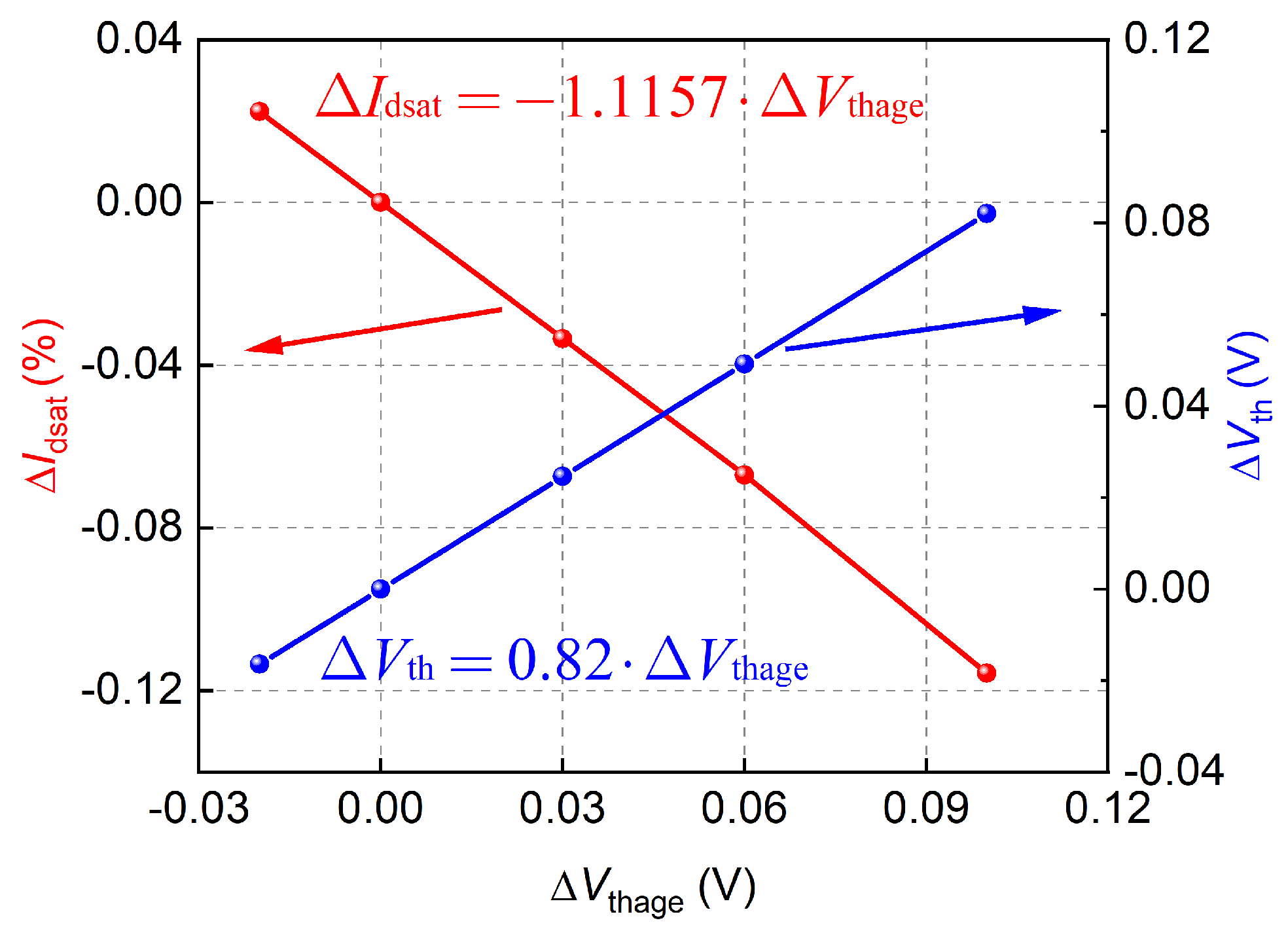
3.1.2. Influence of Threshold Voltage
To quantify the influence of
on
and
, the value of
can be changed, while other parameters remain unchanged, as shown in
Table 2. Similarly, the
and
are the values after changing
. The corresponding degradation of
and
can be obtained. In a group of simulations, when we shifted the threshold voltage of MOSFET transistor about 30 mV (
= 0.03), which causes a shifting in the
of MOSFET transistor about 5.731
. Through other sets of simulations, the coefficient
can be computed from the relation:
When
, there was a shift in the
of the MOSFET transistor of about 24.6 mV. Through other sets of simulations, the
coefficient could be obtained from the following relation:
The specific results are shown in
Figure 1 and
Figure 2:
was only related and proportional to
.
had little effect on it and could be ignored. However,
with
and
, it was inversely proportional to
and proportional to
. Therefore, the relationship between the degradation MOSFET transistor and the aging parameters could be established [
14]:
where
,
,
,
. After the degradation values of MOSFET transistor parameters had been obtained, the
and
in SPICE model could be calculated on the basis of this relationship, and the simulation model of circuit aging could be established.
According to Equations (
4), (
5) and (
16), two simulation parameters,
and
, were calculated. However, when we used the two obtained parameters to reversely deduce the degradation of MOSFET transistor parameters, if the degradation of the MOSFET transistor parameters was greater than 5%, the error was large, as illustrated in
Figure 3. The result shows that the actual test value of
was 8.63%, while the simulation result exceeded 10%, and the error was as high as 19.8%, which is unacceptable for engineering.
3.2. Coefficient Fitting Based on the Variable Control Method
To solve this problem, we studied the correlation between simulation parameters and the degradation of MOSFET transistor parameters. Equation (
16) could achieve parameter conversion via a simple addition when
was only affected by
. The result is shown in
Figure 4, and the error was less than 0.03%. However, when
and
, both had an influence on the
of the MOSFET transistor. In addition to considering the respective influence coefficients on
degradation, there had to be joint influence coefficients on the degradation of
:
The left-hand side of the Equation (
17) is
after MOSFET transistor degradation, and the right-hand side is the
caused by aging parameters
and
, which can be simplified as below:
Equation (
18) shows that there was such a large error because of the omission of the last term and the joint influence of the two parameters on the degradation of
. Thus,
According to the accelerated lifetime model or test, we could obtain the values of
and
. The corresponding
and
could be calculated from Equation (
19). Then, the values of
and
could be changed via the Alter instruction in SPICE to simulate the aging effect of the circuit. The result is shown in
Figure 5. No matter what the degradation value was in the display range, the simulation accuracy was within 0.047%, which is in line with the actual demand.
However, the coefficient matrix is nonlinear and can only be realized by solving nonlinear equations. To facilitate the realization through programming, this paper proposes a second method to calculate the conversion coefficient, which can form a linear matrix that establishes a high-precision simulation model.
3.3. Coefficient Fitting Based on Multiple Systems of Equations
Since
and
both had an influence on the degradation of
, the common influence of the two parameters on
should be considered when extracting the coefficients. Namely,
and
were changed simultaneously, as shown in
Table 3. According to engineering experience, two groups of
and
were determined, and then a simulation was carried out under each group of conditions. The degradation of the MOSFET transistor parameters was acquired via simulation as follows:
By solving for Equation (
20), coefficients
= 0.8945,
= −1.0892 were obtained and entered into Equation (
16) for simulation; the obtained result is illustrated in
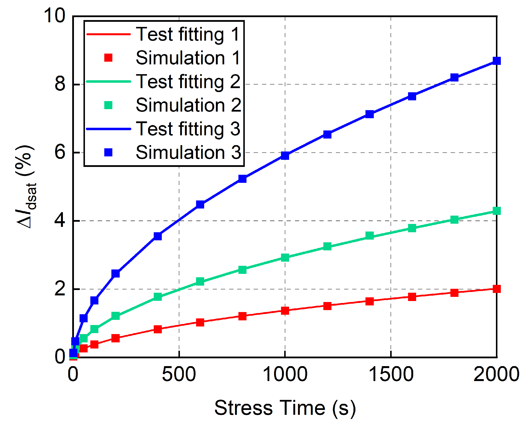
Figure 6. The error of the coefficients extracted through this method was controlled within 0.0961% when simulating the degradation of the MOSFET transistor. This could also meet practical needs, and the program of this approach is straightforward.
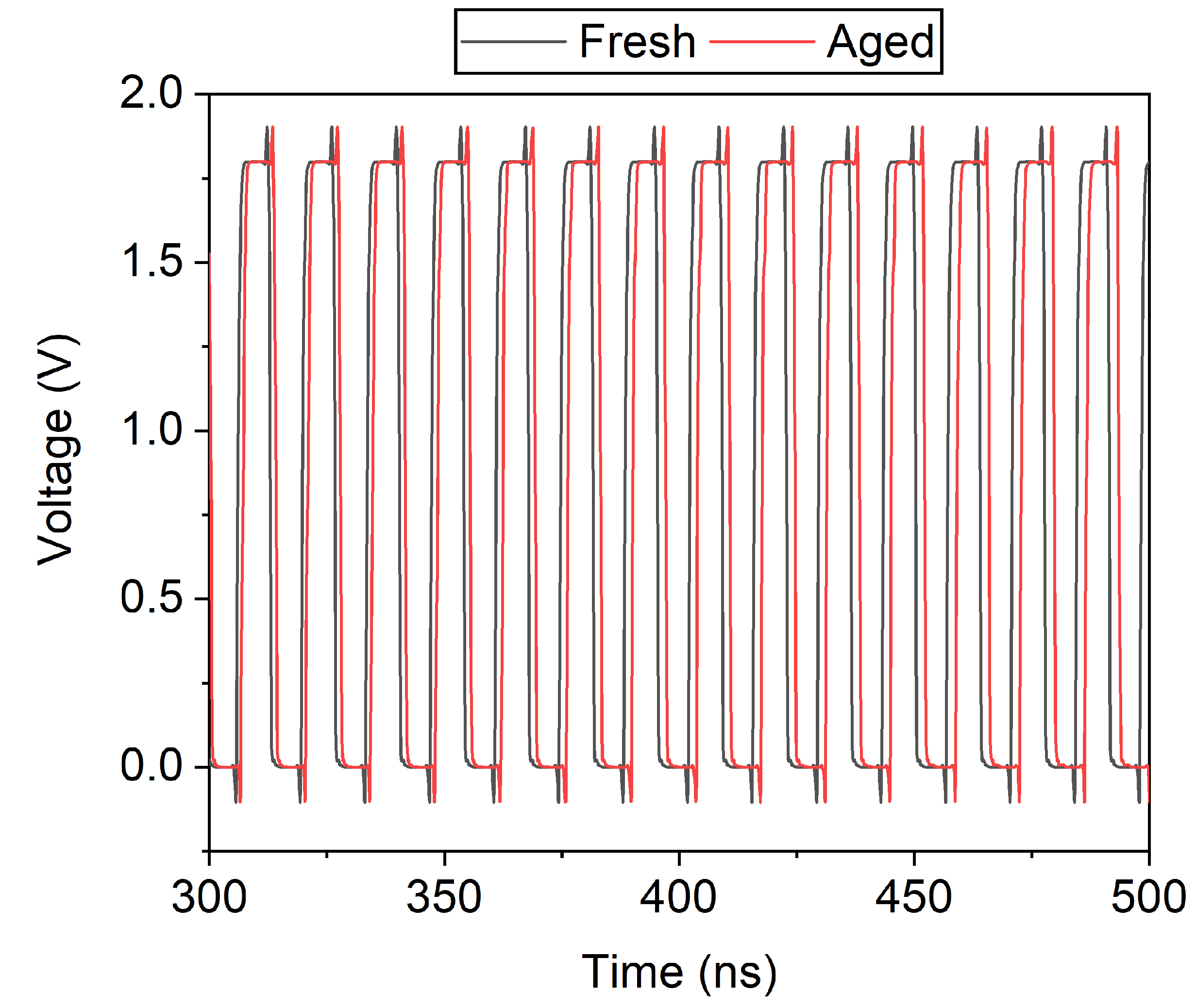
According to the simulation parameters based on multiple systems of equations, we simulated the aging effect (including HCI and NBTI) of the ring oscillator, and its schematic is shown in
Figure 7. We simulated the circuit working in a 125-degree environment for 5 years, and its stress voltage was the normal operating voltage, namely, 1.8 V. Under the influence of the aging effect, the oscillation frequency dropped from 72.84 to 72.69 MHz; the simulation result is illustrated in
Figure 8. This was mainly because of an increase in the
of the MOSFET transistors.
4. Summary and Outlook
There is a large error in the simulation parameters when calculating the MOSFET transistor degradation; thus, it is difficult to establish a high-precision aging model for circuits. To solve this problem, a method for calculating the high-precision fitting coefficient was proposed based on variable control. The coefficients that reflect how the simulation parameters impact MOSFET transistor degradation were extracted separately, and the impact coefficient of interaction was added on the basis of this conception, which also improved the accuracy of the model. However, in order to facilitate the solution with programming, the linear coefficient matrix needed to be established. Therefore, the aging parameters were changed at the same time to obtain their synergistic impact coefficients on the degradation of the MOSFET transistor parameters. The simulation results show that the proposed method is easy to implement while ensuring accuracy, which provides convenience for circuit-level aging simulations. We simulated the aging effect of a 9-order ring oscillator, and the results show that this aging model could predict the lifetime of the circuit.
The current method only applies two SPICE model parameters, namely, threshold voltage and mobility. In the following research, multiple SPICE model parameters could be used to characterize the aging effect (such as adding saturation speed and on-resistance), and other aging effects can be considered to further improve aging simulation accuracy.
Author Contributions
X.Y.: conceptualization, data curation, investigation, methodology, visualization, and writing—original draft, review, and editing. Q.S.: formal analysis, funding acquisition, and writing—review and editing. J.Z.: supervision and validation. C.W.: project administration, resources, and software. M.Y.: data curation and investigation; Y.Z. and S.W.: formal analysis. All authors have read and agreed to the published version of the manuscript.
Funding
This research received no external funding.
Data Availability Statement
The data are easily available if other scientists are interested in reanalyzing the data. The data may also be obtained with the consent of all authors.
Acknowledgments
The authors wish to thank the editor and anonymous referees for their helpful comments in improving the quality of this paper.
Conflicts of Interest
The authors declare no conflict of interest.
Abbreviations
The following abbreviations are used in this manuscript:
| HCI | Hot carrier injection |
| NBTI | Negative bias temperature instability |
| CAD | Computer-aided design |
| DC | Direct current |
| SPICE | Simulation program with integrated circuit emphasis |
References
- Kishida, R.; Asuke, T.; Furuta, J.; Kobayashi, K. Extracting Voltage Dependence of BTI-induced Degradation without Temporal Factors by Using BTI-Sensitive and BTI-Insensitive Ring Oscillators. IEEE Trans. Semicond. Manuf. 2020, 33, 174–179. [Google Scholar] [CrossRef]
- Dounavi, H.; Sfikas, Y.; Tsiatouhas, Y. Periodic Monitoring of BTI Induced Aging in SRAM Sense Amplifiers. IEEE Trans. Device Mater. Reliab. 2019, 19, 64–72. [Google Scholar] [CrossRef]
- Chen, W. Electrothermal Effects on Hot-Carrier Reliability in SOI MOSFETs—AC Versus Circuit-Speed Random Stress. IEEE Trans. Electron. Devices 2016, 63, 3669–3676. [Google Scholar] [CrossRef]
- Son, D.; Park, J.; Shin, H. Investigation and Compact Modeling of Hot-Carrier Injection for Read Disturbance in 3-D NAND Flash Memory. IEEE Trans. Electron. Devices 2020, 67, 2778–2784. [Google Scholar] [CrossRef]
- Zhang, L.; Ma, C.; Xiao, Y.; Zhang, H.; Lin, X.; Chan, M. A Dynamic Time Evolution Method for Concurrent Device-Circuit Aging Simulations. IEEE Trans. Electron. Devices 2019, 66, 184–190. [Google Scholar] [CrossRef]
- Puschkarsky, K.; Reisinger, H.; Rott, G.A.; Schlünder, C.; Gustin, W.; Grasser, T. An Efficient Analog Compact NBTI Model for Stress and Recovery Based on Activation Energy Maps. IEEE Trans. Electron. Devices 2019, 66, 4623–4630. [Google Scholar] [CrossRef]
- Parihar, N.; Goel, N.; Mukhopadhyay, S.; Mahapatra, S. BTI Analysis Tool—Modeling of NBTI DC, AC Stress and Recovery Time Kinetics, Nitrogen Impact, and EOL Estimation. IEEE Trans. Electron. Devices 2018, 65, 392–403. [Google Scholar] [CrossRef]
- Santana-Andreo, A.; Martín-Lloret, P.; Roca, E.; CastroLopez, R.; Fernandez, F.V. Characterization and analysis of BTI and HCI effects in CMOS current mirrors. In Proceedings of the 2022 18th International Conference on Synthesis, Modeling, Analysis and Simulation Methods and Applications to Circuit Design (SMACD), Villasimius, Italy, 12–15 June 2022; pp. 1–4. [Google Scholar]
- Li, X.; Qin, J.; Bernstein, J.B. Compact Modeling of MOSFET Wearout Mechanisms for Circuit-Reliability Simulation. IEEE Trans. Device Mater. Reliab. 2008, 8, 98–121. [Google Scholar] [CrossRef]
- Eslahi, H.; Albahrani, S.A.; Mahajan, D.; Khandelwal, S. An Analytical Model for Hot Carrier Induced Long-Term Degradation in Power Amplifiers. IEEE Trans. Comput.-Aided Des. Integr. Circuits Syst. 2020, 39, 2000–2005. [Google Scholar] [CrossRef]
- Yibo, J. Study on Non-Monotonic Hot Carrier Degradation and Predictive Model for Long Drift Region Double Field Shields LDMOS. IEEE Trans. Device Mater. Reliab. 2018, 18, 404–411. [Google Scholar] [CrossRef]
- Yang, X.; Sang, Q.; Zhang, J.; Wang, C.; Yu, M.; Zhao, Y. A high-efficiency aging test with new data processing method for semiconductor MOSFET transistor. Microelectron. Reliab. 2023, 143, 114940. [Google Scholar] [CrossRef]
- Galadi, A. Accurate power MOSFET models including quasi-saturation effect. J. Comput. Electron. 2016, 15, 619–626. [Google Scholar] [CrossRef]
- Sang, Q.; Yang, X.; Zhang, J.; Wang, C.; Yu, M.; Zhao, Y. A multi-parameter fitting method based on matrix transformation for MOSFET transistor aging modeling. Microelectron. Reliab. 2023, 142, 114913. [Google Scholar] [CrossRef]
| Disclaimer/Publisher’s Note: The statements, opinions and data contained in all publications are solely those of the individual author(s) and contributor(s) and not of MDPI and/or the editor(s). MDPI and/or the editor(s) disclaim responsibility for any injury to people or property resulting from any ideas, methods, instructions or products referred to in the content. |
© 2023 by the authors. Licensee MDPI, Basel, Switzerland. This article is an open access article distributed under the terms and conditions of the Creative Commons Attribution (CC BY) license (https://creativecommons.org/licenses/by/4.0/).

 ,
, 


