Communication

Heavy Ion Induced Degradation Investigation on 4H-SiC JBS Diode with Different P+ Intervals

1
Institute of Microelectronics of the Chinese Academy of Sciences, Beijing 100029, China
2
University of Chinese Academy of Sciences, Beijing 100049, China
3
State Key Laboratory of Advance Power Semiconductor Device, Zhuzhou CRRC Times Semiconductor Company Ltd., Zhuzhou 412001, China
*
Authors to whom correspondence should be addressed.
Electronics 2023, 12(9), 2133; https://doi.org/10.3390/electronics12092133
Submission received: 19 April 2023 / Revised: 4 May 2023 / Accepted: 5 May 2023 / Published: 6 May 2023
(This article belongs to the Special Issue New Insights in Radiation-Tolerant Electronics)

Abstract

:
The heavy ion radiation response and degradation of SiC junction barrier Schottky (JBS) diodes with different P+ implantation intervals (S) are studied in detail. The experimental results show that the larger the S, the faster the reverse leakage current increases, and the more serious the degradation after the experiment. TCAD simulation shows that the electric field of sensitive points directly affects the degradation rate of devices with different structures. The large transient energy introduced by the heavy ion impact can induce a local temperature increase in the device resulting in lattice damage and the introduction of defects. The reverse leakage current of the degraded device is the same at low voltage as before the experiment, and is gradually dominated by space-charge-limited-conduction (SCLC) as the voltage rises, finally showing ballistic transport characteristics at high voltage.

1. Introduction

Due to its excellent material properties such as high saturation drift velocity, high breakdown electric field, and high thermal conductivity, silicon carbide (SiC) is very suitable for power electronic devices, especially for extreme applications such as high voltage and high temperature [1]. SiC power devices have the advantages of low loss, high power density, and fast switching speed, which are widely used in power grids, high-speed rail, new energy vehicles, etc. [2]. In aerospace application, SiC power devices are expected to replace Si power devices in the future in power processing units, motor drives, and other aerospace power systems to reduce system weight while improving the energy conversion efficiency of the system [3]. However, despite its excellent performance, the application of SiC power electronic devices in the irradiation environment remains to be proven, as research shows that the reliability of devices in the irradiation environment is less than expected [4]. Under the irradiation of high-energy protons or heavy ions, SiC power devices are susceptible to single event effect that can lead to device degradation or burnout [5,6,7,8,9,10,11,12,13,14,15].
The heavy ion irradiation response of SiC power electronic devices can be divided into three regions [5]. At low reverse bias voltage region, they work normally. In the medium voltage region, the devices show degradation exhibiting increased leakage current. Under high voltage, the devices will burn out. The degradation and burnout threshold voltages are strongly dependent on the reverse bias voltage and the linear energy transfer (LET) of the heavy ion. This has been validated in both junction barrier Schottky (JBS) diodes and metal oxide semiconductor field effect transistors (MOSFETs), implying a commonality in their heavy ion irradiation response [6,7,8]. Therefore, it is more convenient to investigate the complex mechanism in the irradiation response of SiC power devices using Schottky diodes, which have a relatively simple structure. Currently, related research mainly focuses on hardening design and failure mechanism. The hardened design is mainly studied by TCAD simulation but has not been reported in practice [6,9,10,11]. The study of failure mechanism is significant as it can provide theoretical guidance for hardening design. The internal structure of the device has a dramatic effect on its failure mode. However, the current experimental studies are mainly focused on commercial devices [12,13,14,15,16], which cannot investigate further on the structure of the devices, since usually, this information is commercially confidential. Therefore, there are few studies on the effect of device structure on heavy ion irradiation characteristics and the discrepancy of irradiation characteristics between different structures is not yet clear.
In this paper, 1200 V SiC JBS diodes with different structures were irradiated by heavy ions. Experimental results show that the bigger the P+ implantation interval (S), the more severe the corresponding device degradation. The TCAD simulation study found that the larger the S, the harsher the electric field and temperature in the epitaxial layer, which is consistent with the experimental results. Finally, the reverse electrical characteristics of the degraded devices with different structures are fitted and analyzed to explain the leakage mechanisms of the devices at high, medium, and low operating voltages, respectively.

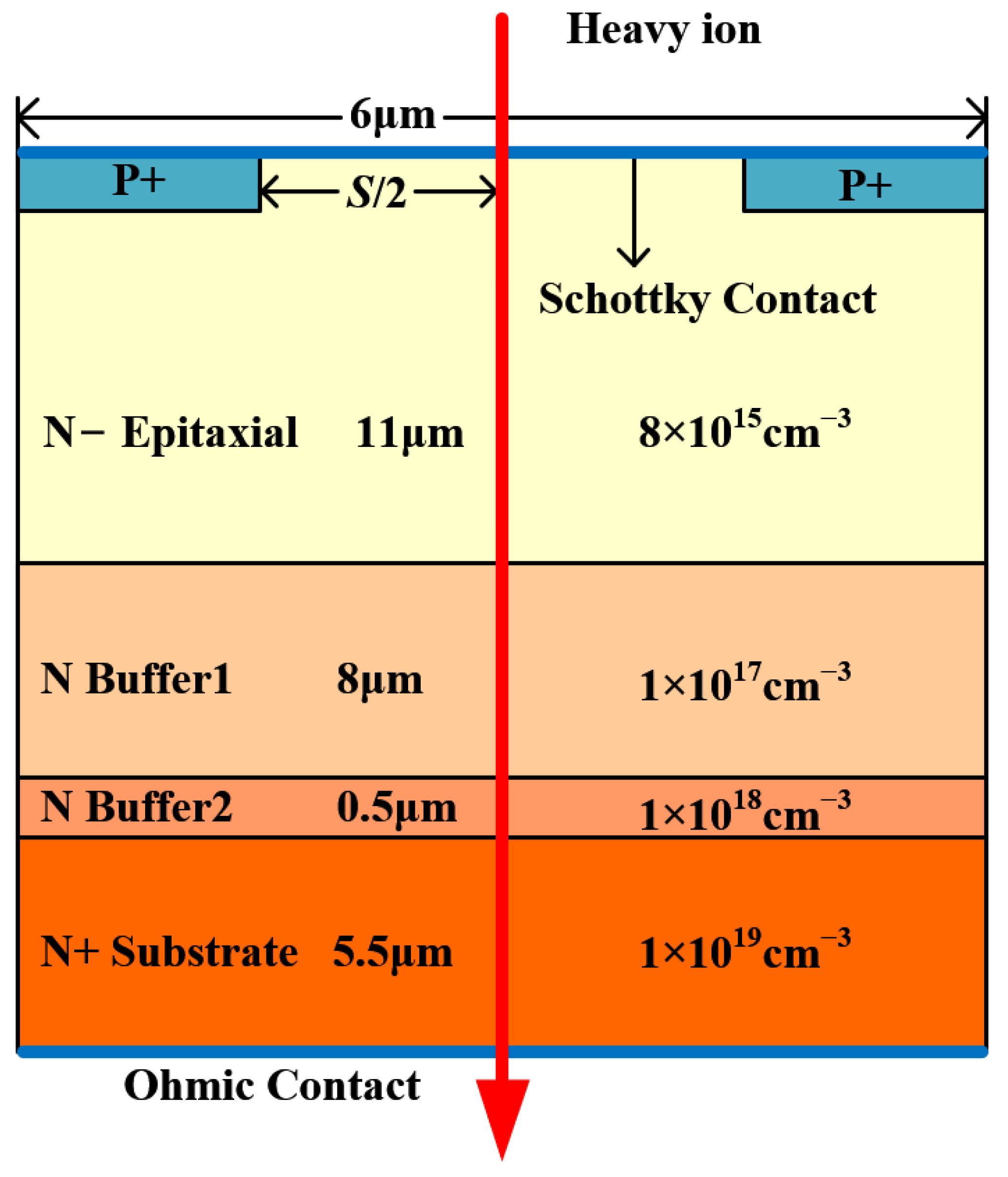
2. Experiment and Simulation Setup

To investigate the heavy ion irradiation response and degradation of SiC JBS diodes with various structures, three kinds of 1200 V JBS diodes with different P+ implantation intervals S were fabricated. The S of DUT1, 2, and 3 are 2, 3, and 4 μ m, respectively, and the P+ implantation windows are all 2 μ m. The active region is a square geometry with rounded corners and has an area of 0.09 cm 2 . The devices are fabricated on an N-type 4H-SiC wafer which has an epitaxial layer, two buffer layers, and a 350 μ m substrate supplied by EpiWorld International Company Ltd., Xiamen, China. The specific structure and parameters are shown in Figure 1.
Standard RCA cleaning processes were utilized on the SiC wafer before sacrificial oxidation was used to improve the SiC interface condition. The oxide layer was etched with a dilute HF solution, and the backside ohmic contact was created by depositing a 200-nm-thick Ni film, followed by rapid thermal annealing (RTA) at 950 °C for 120 s in nitrogen ambient. Thereafter, a 200-nm-thick Ti layer was deposited by e-beam evaporation on the surface of the SiC epitaxial layer. A typical photolithography procedure was used to create the Schottky connections. The DUTs are in open TO-257 metal packages to ensure that heavy ions can penetrate the epitaxial layer of the devices.
Heavy ion irradiation experiments were performed at the Institute of Modern Physics, Chinese Academy of Sciences in Lanzhou, China using Tantalum ions set at a device surface energy of 1912.1 MeV with flux of 6000/cm 2 ·s. The surface LET is 79.6 MeV·cm 2 /mg for SiC and the range is 75.6 μ m calculated by SRIM [17]. During the experiments, the DUTs were kept at room-temperature. The device current was monitored by a Keithley 2657A High Power System Source Meter Instrument. The current compliance was set at 2 mA. An Agilent B1505A Semiconductor Device Parameter Analyzer was used to measure the forward and reverse IV characteristics before and after the experiments.
For the three structures, firstly, one device of each structure is selected to determine the degradation threshold voltage and burnout voltage. With an initial bias voltage of 50 V, each run is increased by 50 V until the device leakage reaches the current compliance. The fluence of each run is 10 5 /cm 2 . Subsequently, a bias voltage of 250 V at which all three structures degrade was selected and two devices of each structure were irradiated to 10 6 /cm 2 at this bias voltage to observe the degradation phenomenon.
To facilitate the observation of the internal conditions of the device, Sentaurus TCAD simulation software from Synopsys was used to analyze the heavy ion response [18]. The schematic cross-sectional view of the JBS diode is shown in Figure 1. In the 2D simulation, the carrier flux at the structure boundary is set to zero by default. Therefore, the cell width of the device is set to 6 μ m to exclude the effect of various cell widths. The width of the Schottky contact S is set to 2–4 μ m, corresponding to the width of P+ implantation on both sides is 2–1 μ m. The P+ profile was extracted by secondary ion mass spectrometry (SIMS) and loaded into the simulation. In addition, the default thickness of the structure in the 2D simulation is 1 μ m.
To predict the device response more precisely, the typical physics models for SiC devices were applied, as used in the published papers [19,20]. Due to the presence of a heavy doping region (P+), the Fermi distribution is used. The recombination process is described by the Shockley–Read–Hall (SRH) recombination and Auger recombination models. The avalanche process in the high electric field is described by the Okuto-Crowell model [21]. The mobility models take into account high field saturation, temperature, and doping dependence. The Slotboom model [22] is used to describe bandgap narrowing. The incomplete ionization model [23] and anisotropic model in mobility [24] and avalanche [25] are also considered. The barrier lowering model [26] is applied to characterize reverse leakage current.
The heavy ion model is the most important part used to predict the transient response of heavy ion impact. In this model, electron-hole pairs generated along the vertical ion track by heavy ions are computed using spatial and temporal Gaussian distributions. The generated charges are assumed uniformly distributed along the ion track [27]. The initial charge generation time is set at 5 ps. The characteristic time of the temporal Gaussian function is 2 ps [19]. The incident point is chosen at the middle of the Schottky contact, as shown by the red arrow in Figure 1, which is considered to be the most sensitive point of the device [13,28]. The ion track radius is set to 0.1 μ m [6] and the depth is long enough to penetrate the entire device. In this simulation, the unit of LET is pC/ μ m. For SiC (electron-hole pair creation energy is 7.8 eV), 1 pC/ μ m = 151 MeV·cm 2 /mg [27], so this value is set to 0.5272 pC/ μ m. In the transient process of heavy ion impact, the electrothermal coupling behavior is involved. Therefore, the thermodynamic model is also included [19].

3. Result and Discussion

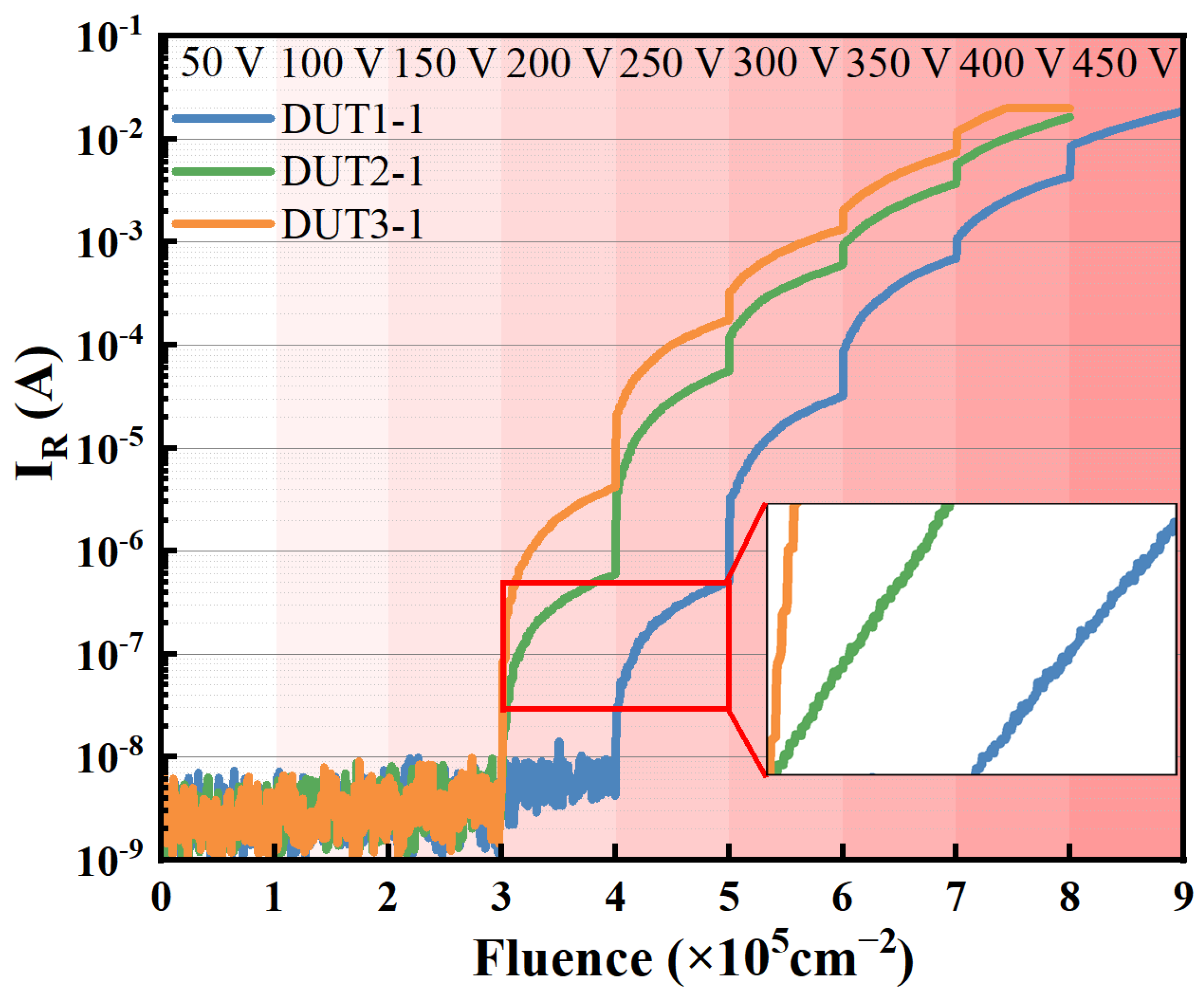
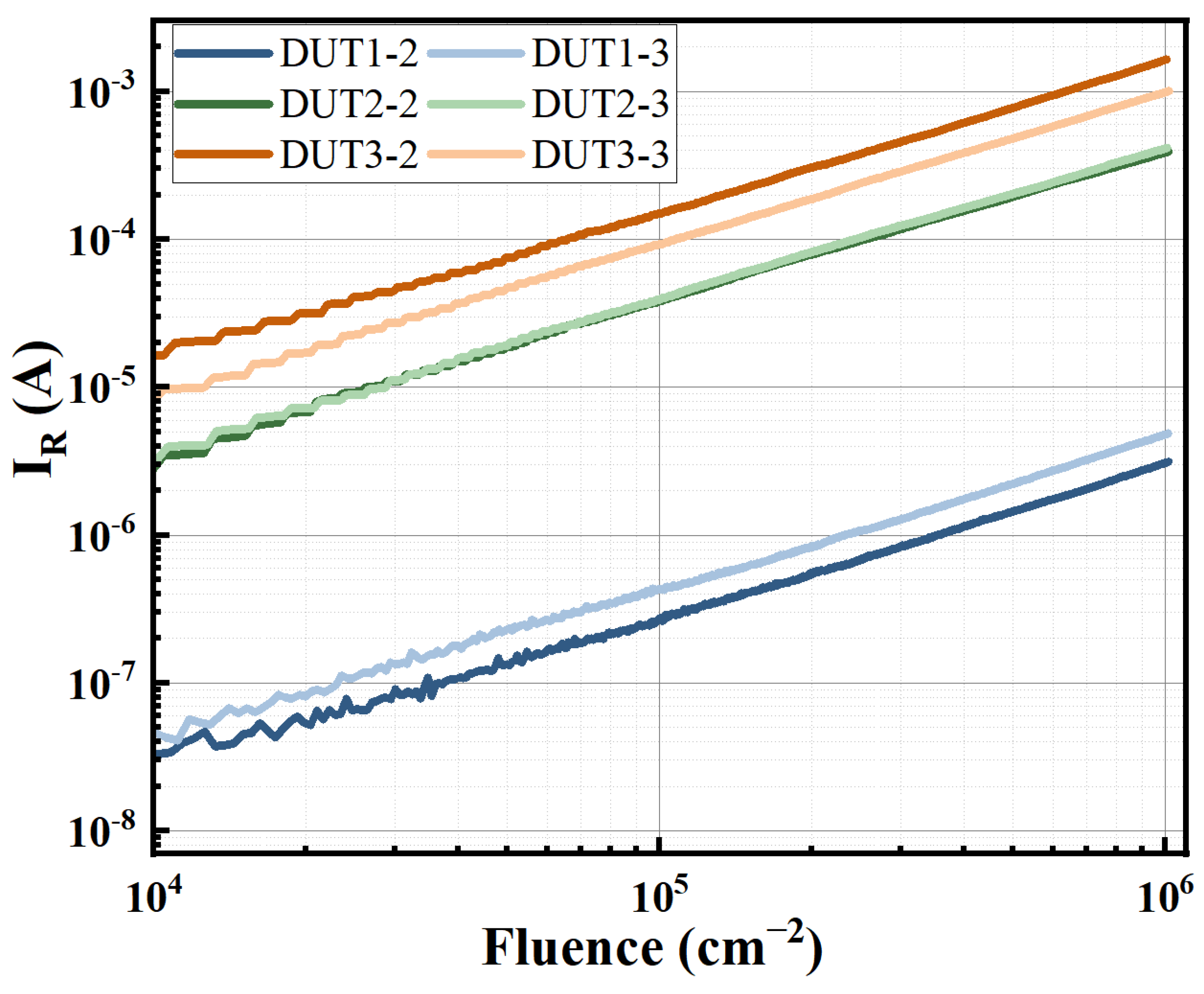
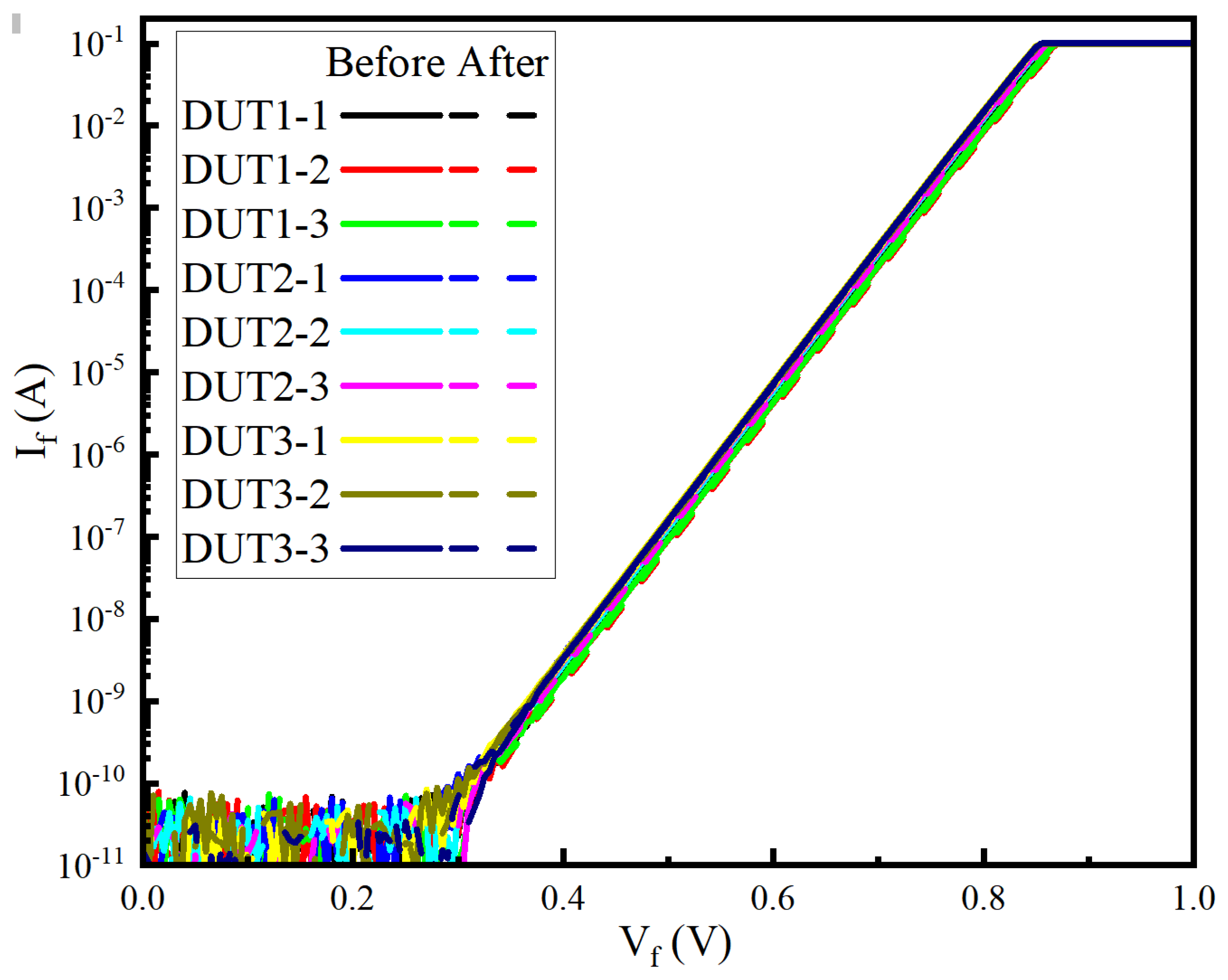
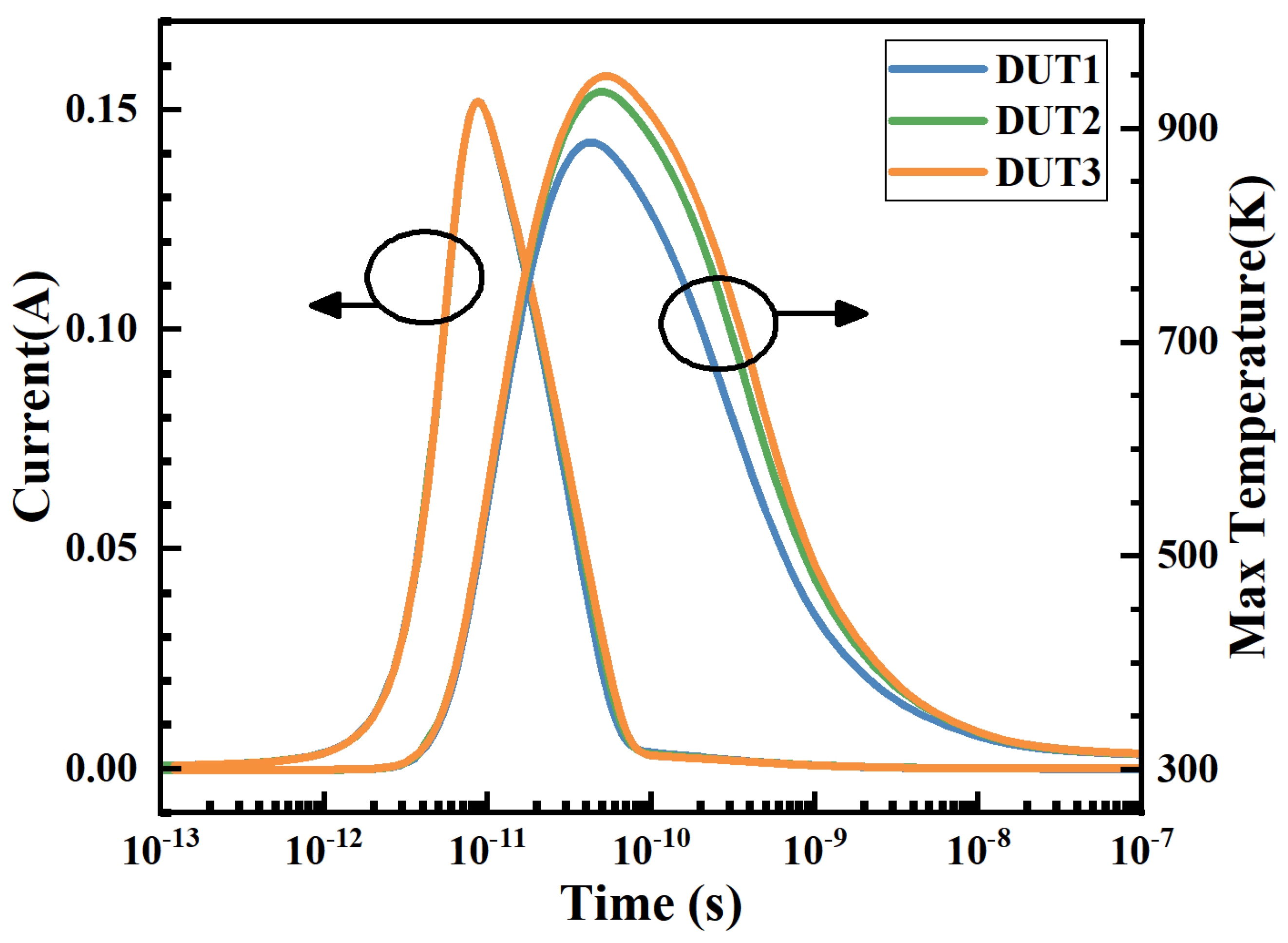
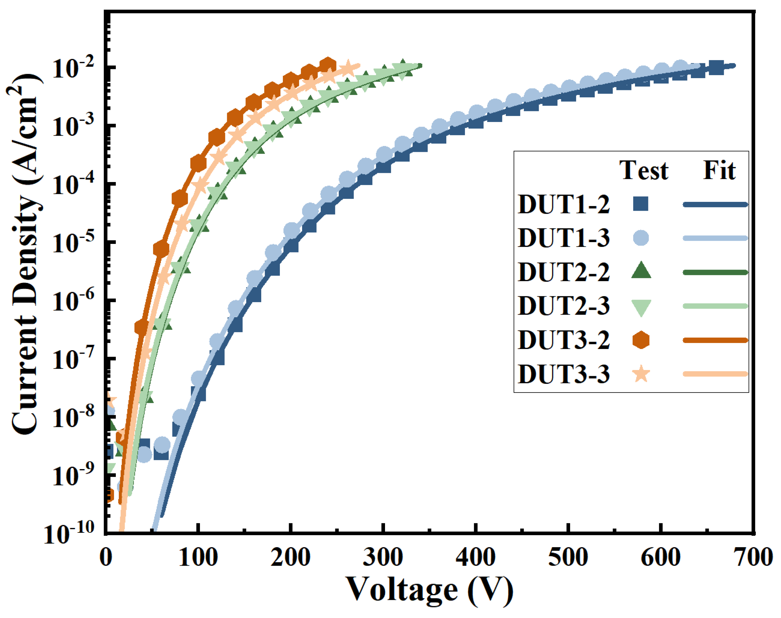
3.1. Experiment Results

The purpose of the first experiment was to determine the degradation and burnout threshold voltage of the three structures. The leakage current of the DUTs in the experiment is shown in Figure 2. DUT1-3 start to degrade significantly at 250 V, 200 V, and 200 V, respectively, with leakage currents rising gradually with increasing ion fluence and bias voltage. Therefore, the bias voltage of the DUTs for the constant bias experiment is set at 250 V to investigate the effect of structures on the heavy ion response. The variation of the current during the constant bias irradiation is shown in Figure 3. At this bias voltage, the current of all DUTs increases linearly with increasing ion fluence and the current degradation rate of two DUTs of the same structure is close. Moreover, the degradation rate of the DUTs at this bias becomes larger as S increases.
The static characteristics of the DUTs were measured before and after the experiments. The forward characteristics are shown in Figure 4. The forward output curves of all DUTs before and after the experiments are highly overlapping, indicating that the forward characteristics of the devices are not affected by the heavy ion degradation. In our previous study, it was demonstrated in more detail that the degradation caused by the single event effect did not affect the forward output characteristics of the device [29]. The experiment mainly affects the reverse characteristics of the DUTs. The reverse leakage currents of the three kinds of DUTs all appear to increase. The results are shown in Figure 5. The reverse leakage current shows a positive correlation with S. The larger S, the higher the reverse leakage current. Through the above analysis, it can be concluded that the larger the degradation rate, the higher the reverse leakage current and the more serious the degradation.
It is worth noting that the leakage current curves after the experiment in Figure 5 can be divided into three regions. In the low-voltage region, the curves before and after the experiment almost overlap, implying that degradation does not affect the current characteristics in this region. After a turning voltage V t , the reverse leakage current increases dramatically. V t for DUT1-3 is about 85 V, 35 V, and 25 V, respectively. Finally, the current growth rate slows down and tends to saturate. Further analysis of this phenomenon will follow in the discussion section.

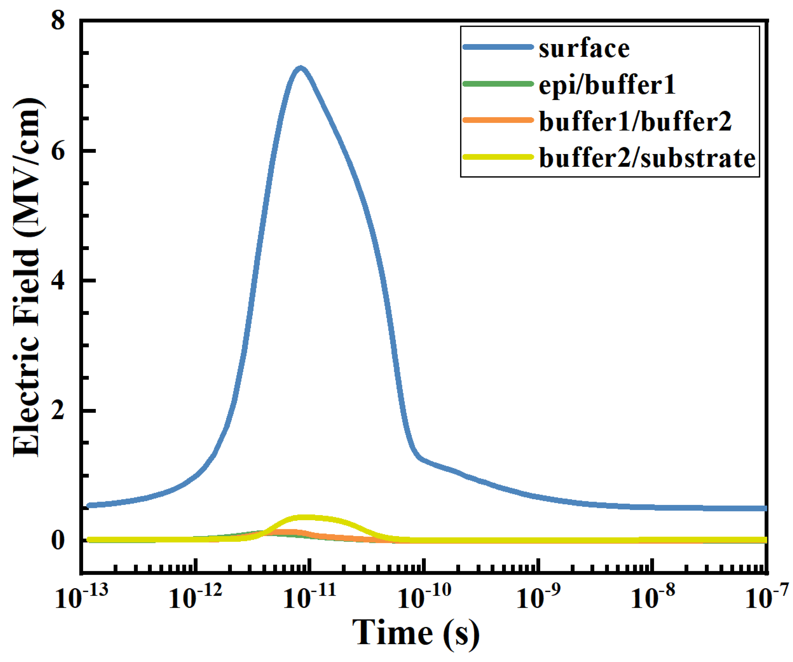
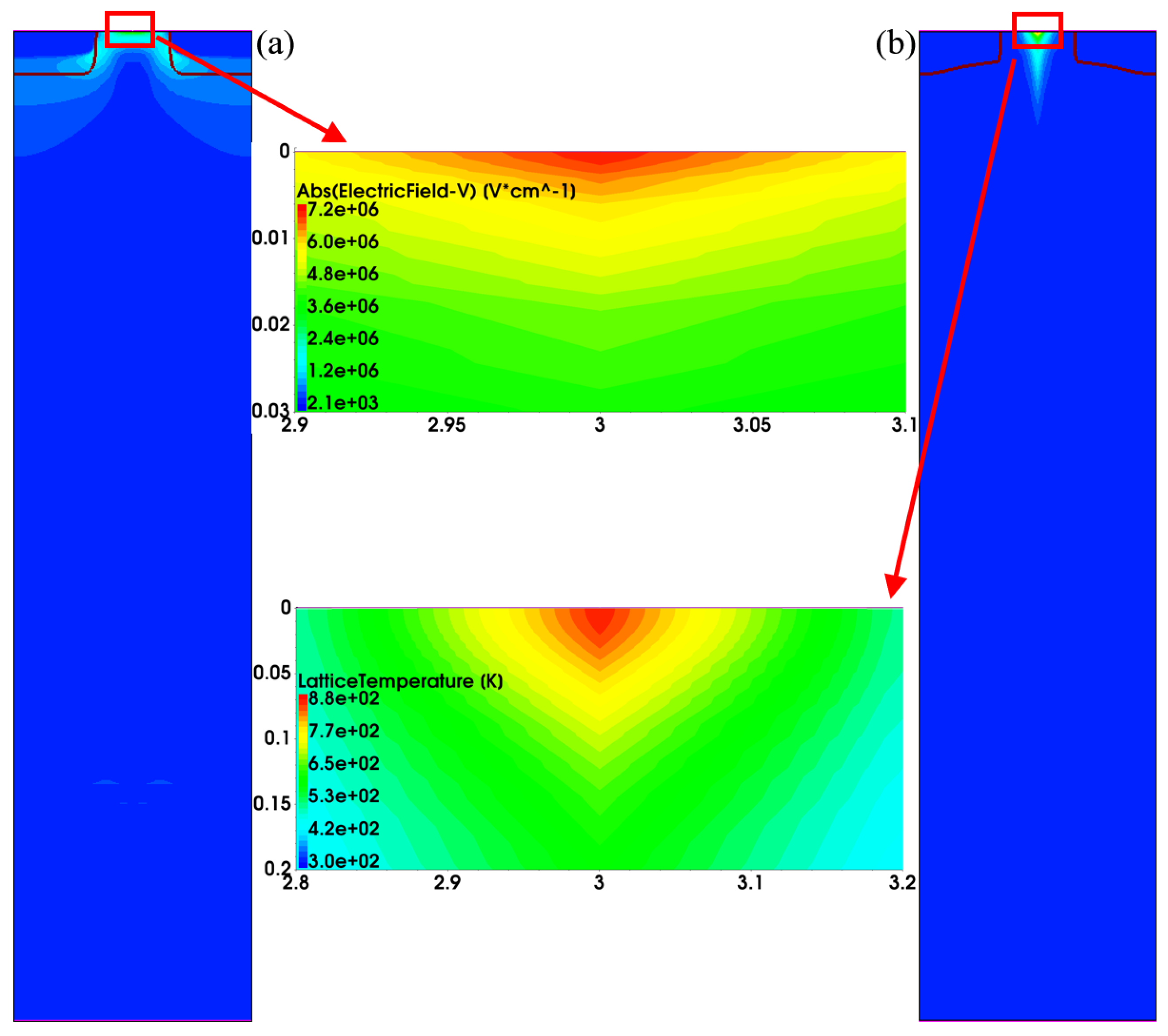
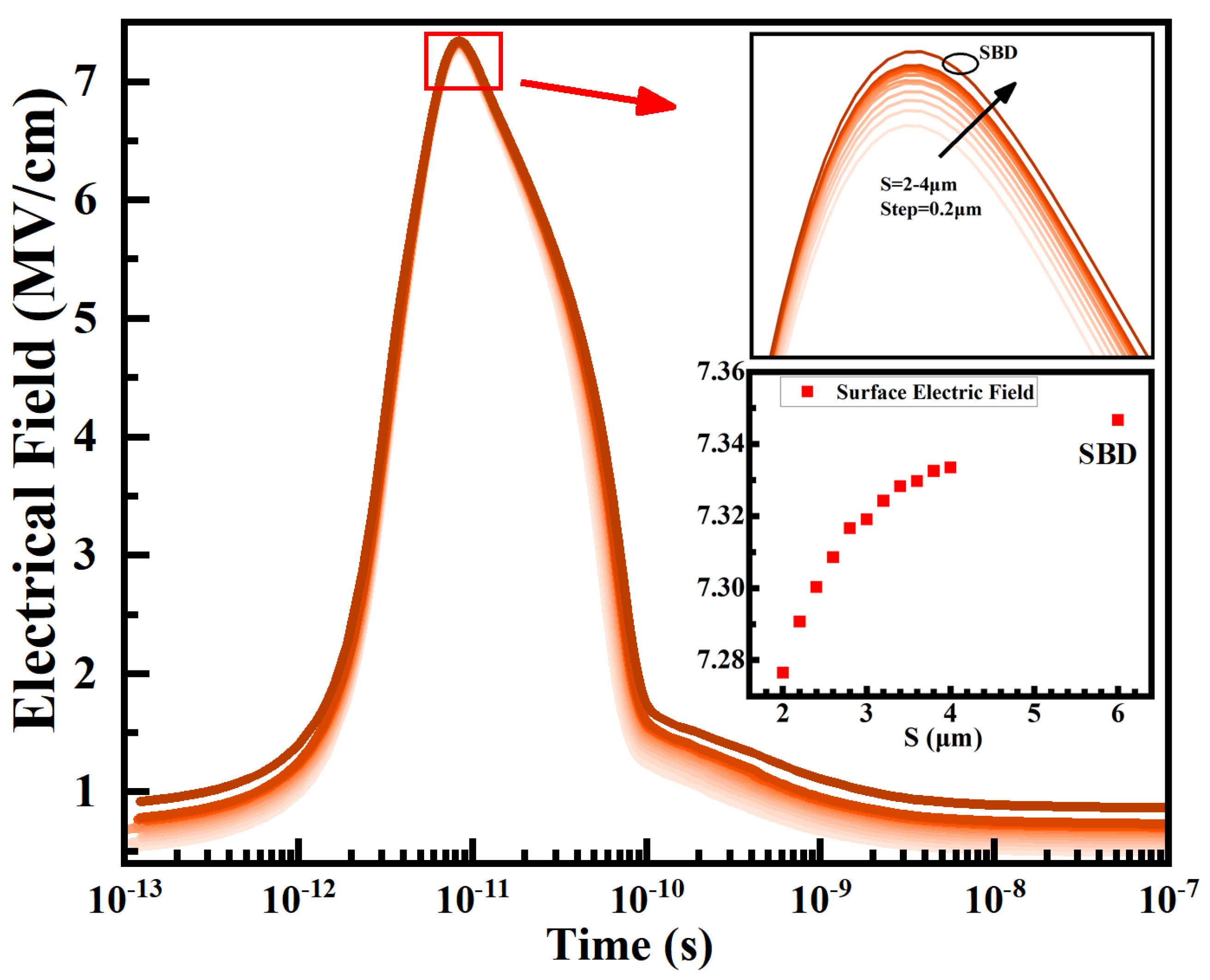
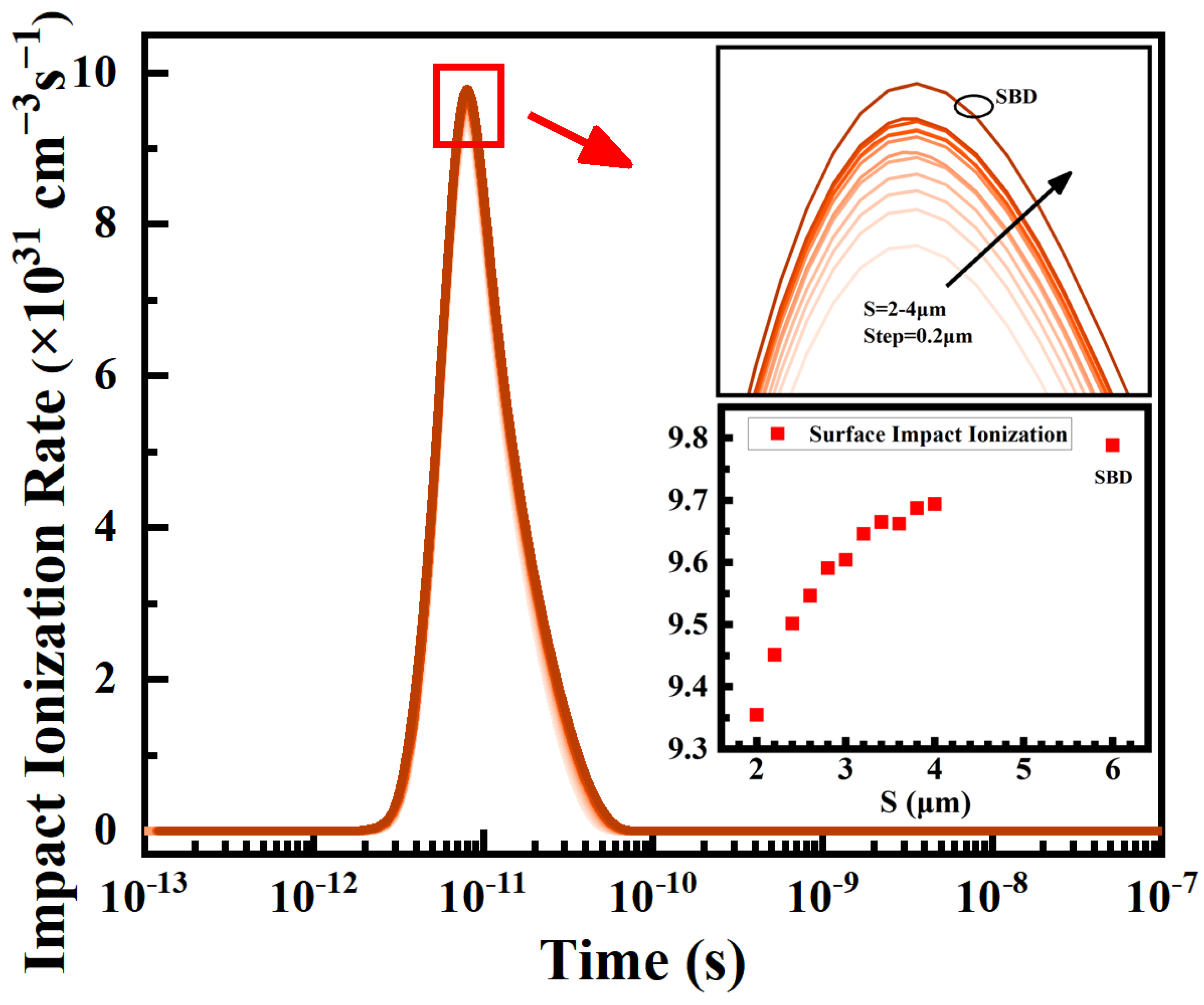
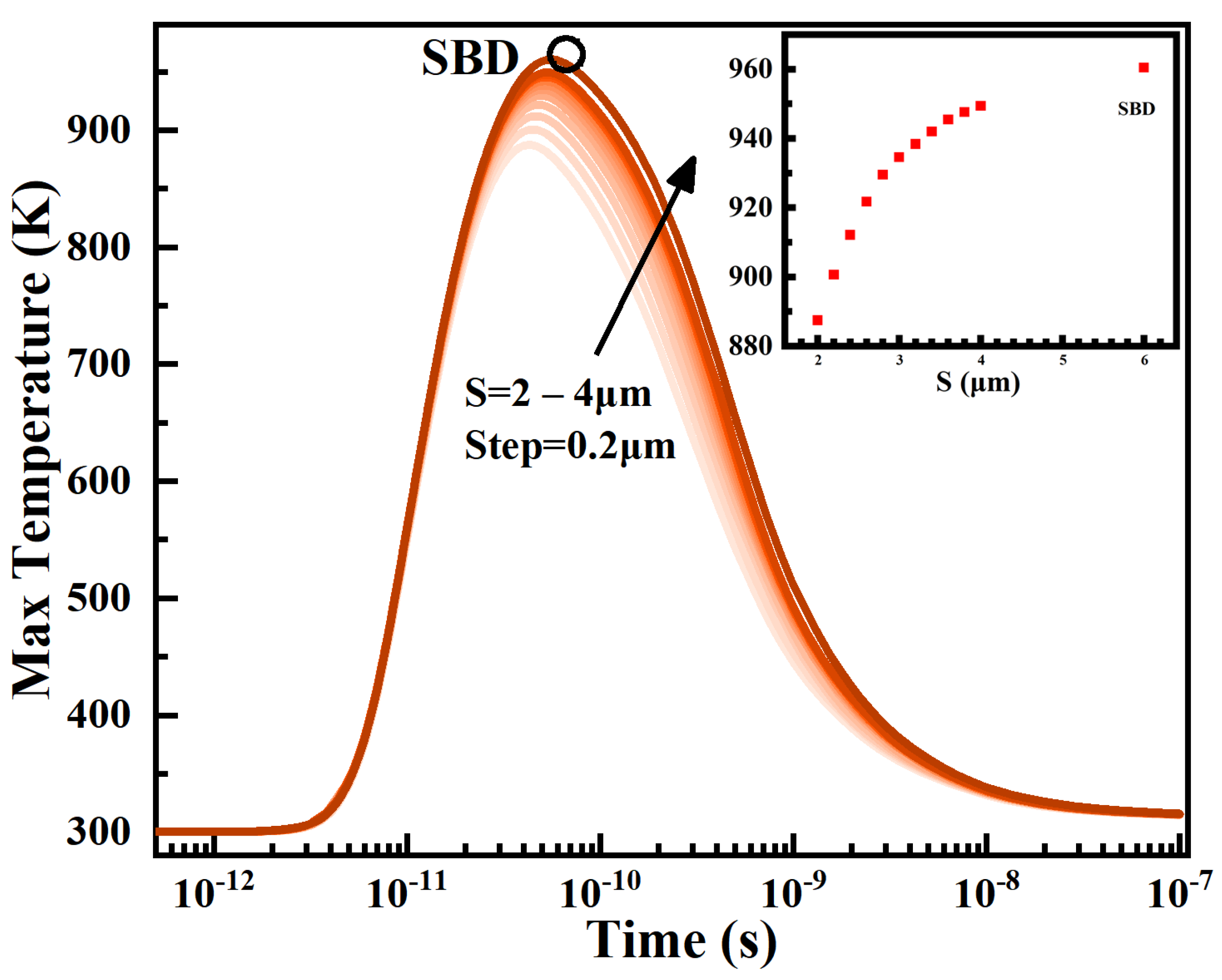
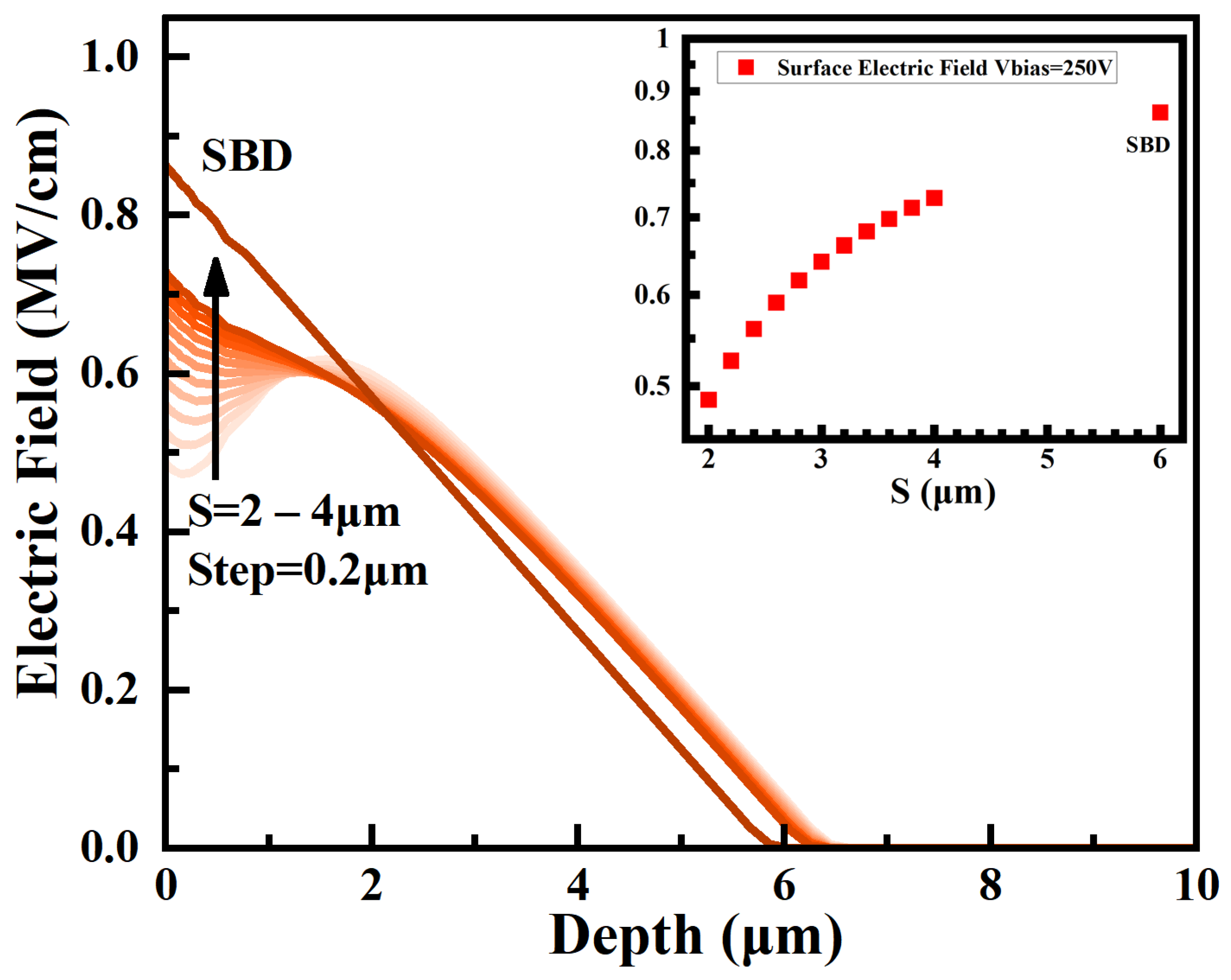
3.2. Simulation Result and Analysis

TCAD simulations were built to investigate the influence of different S on the heavy ion impact response. Figure 6 shows the heavy ion response of DUTs under a bias of 250 V. The left axis represents the cathode current and the right axis represents the maximum lattice temperature of the devices. As shown in the current response curve, the current rises dramatically after ion incidence and all currents reach peaks at 9 ps. Thereafter, the current gradually decreases until it disappears at about 200 ps. The temperature response shows a delay relative to the current and also rises rapidly, peaking at about 50–60 ps, followed by a rapid decrease and returning to room temperature gradually after 10 ns. The simulation results are close to those of [20,30].
When the ions incident into the device, a large amount of energy is instantaneously introduced along the ion track, resulting in the ionization of a large number of electron-hole pairs. Driven by the electric field, the electrons drift toward the cathode and the holes drift toward the anode. Eventually, electrons pile up at the buff2/substrate junction and holes pile up below the Schottky interface. The high charge accumulation leads to a high electric field at these two locations. Figure 7 shows the electric field evolution at the surface and junctions of DUT1. The electric field at the surface reaches its peak value of 7.3 MV/cm at 9 ps. Note that this time is exactly when the device current reaches its peak and that the electric field is particularly concentrated in a very small region less than 10 nm below the Schottky interface, as shown in Figure 8a. Such a high electric field greatly enhances the impact ionization, which leads to a subsequent fast increase in temperature, the lattice temperature peaking at 50 ps, as shown in Figure 8b.
In Figure 7, note the presence of an electric field peak at the Buffer2/substrate junction at 10 ps. This is caused by the accumulation of electrons here. In contrast with previous studies [20], the electric field peak at this place was alleviated, which was attributed to the addition of a buffer layer. Therefore, the area below the Schottky interface becomes the most sensitive region of the JBS diode. The subsequent analysis is focused on this region.
A more detailed simulation was performed to compare the effect of the Schottky contact width changes with higher resolution. Setting other conditions constant, S is increased from 2.0 μ m to 4.0 μ m in steps of 0.2 μ m, while a Schottky barrier diode (SBD) without P+ implantation is also considered, whose S is set to 6.0 μ m. The evolution of the electric field below the Schottky interface for each device is shown in Figure 9. With the gradual increase of S from 2–4 μ m, the peak electric field gradually increases from 7.277 MV/cm to 7.333 MV/cm, reaching 7.346 MV/cm in the case of the SBD. High electric fields directly lead to large impact ionization rate which is proportional to the seventh power of the electric field [31]. The peak of the impact ionization rate increases with S from 9.36 × 10 31 cm 3 s 1 to 9.69 × 10 31 cm 3 s 1 , reaching 9.79 × 10 31 cm 3 s 1 in the SBD, as shown in Figure 10. Impact ionization generates a large amount of heat in the local region, leading to a subsequent rapid increase of the lattice temperature [16]. As shown in Figure 11, the peak lattice temperature of the device gradually increases from 887.4 K to 949.4 K with increasing S and reaches 960.5 K in the SBD.
From the simulation results, the fundamental source of the different peak temperatures is the excessive concentration of the local electric field. Compare this with the electric field inside the device at 250 V under normal reverse operation, as shown in Figure 12. With the increase of S, the depletion layer formed by P+ implantation is less protective to the Schottky interface. At the same bias voltage, the electric field under the Schottky interface gradually increases as S increases. The huge transient energy introduced by the heavy ion is overlapped with a larger surface electric field, leading to a harsher situation in the device, causing subsequent higher transient lattice temperature. Localized high temperature can cause disorder to the periodic arrangement of the lattice, introducing defects that cause increased leakage current and degradation of the device [13,16,32].

3.3. Leakage Current Mechanism Discussion

As shown in Figure 5, all DUTs exhibit similar degradation characteristics for reverse leakage current, which has been mentioned in Section 3.1. In the low-voltage region, the leakage currents of the degraded DUTs are identical to the results of the pre-experimental measurements. This means that irradiation does not affect the current transport processes in this voltage region, where the leakage current is dominated by the thermionic emission and barrier lowering [33].
With the reverse bias voltage greater than V t , the leakage current rises sharply and is consistent with the space-charge-limited-conduction (SCLC) mechanism. Javanainen modeled degraded devices after heavy ion irradiation by SCLC for the first time [12]. Heavy ion irradiation generates current micro-paths in the device and the linear increase of leakage current is a consequence of path accumulation. The degenerated device is equivalent to a conventional SBD connected in parallel with two series voltage sources that obey
I = k 1 V 1 n ,
I = k 2 V 2 3 / 2 ,
The total reverse current is:
I = k 1 V Bias I / k 2 2 / 3 n ,
In the case of (1), the current transport in the fast-rising current region is due to SCLC considering traps [34]. The traps present an exponential distribution on the energy band.
N t exp E / k T c ,
where T c = (n − 1)·T, T c represents the characteristic temperature for trap distribution and T is the ambient temperature, The larger n indicates that the trap distribution decreases more slowly with energy. In the case of DUTs in this experiment, the reverse leakage curves fitted using (1), (2), and (3) are shown in Figure 13 and the list of fitted parameters is shown in Table 1. The value of n is 7.70–8.87, corresponding to T c of 2010–2361 K, which is a relatively high value. The current in the high-voltage region is consistent with ballistic transport, which describes the maximum current of the SCLC in a scatter-free environment. The above results are very close to those in [12].
It is noticed that as S increases, n decreases while k 1 and k 2 increase, which is related to the structural parameters. The different S causes the different percentage of Schottky contact area of the device. This is another reason for the more severe degradation of devices with larger S. More experiments need to be prepared to distinguish the effects caused by the electric field and Schottky contact area ratio, respectively.
In summary, the current characteristics of the degraded device can be described as follows: The current is mainly dominated by thermionic emission and barrier lowering before V t where the SCLC current is too small to be considered. As the bias voltage rises gradually, leakage current is dominated by SCLC, and finally reaches saturation at high bias voltage.

4. Conclusions

In this paper, heavy ion irradiation experiments were conducted using JBS diodes with different P+ implantation intervals. The results show that the larger the S, the lower the degradation threshold voltage of the device, and the more vulnerable to damage in the radiation environment. The TCAD simulation reveal that after heavy ion impact, the region below the Schottky interface and at the buff2/substrate junction is sensitive. With the buffer layer added, the electric field at the buff2/substrate junction is reduced and the area below the Schottky interface becomes the spot to focus on. It is found that the peak electric field below the Schottky interface increases with S in transient response, which corresponds to the trend of the electric field at this location with S under normal operation. The larger electric field leads to a higher impact ionization rate in this region, resulting in a rapid increase in lattice temperature. Defects introduced by high temperatures are the fundamental reason for device degradation. The leakage current mechanism of the degraded devices are divided in the three regions. In the low-voltage region there is no degradation and the leakage current is determined by the thermionic emission and barrier lowering. Subsequently, leakage current dramatically increases due to SCLC. Eventually, the current gradually saturates. The experiments combined with simulation analysis suggest that the surface electric field can be alleviated by structural design to enhance the heavy ion irradiation resistance of the device, which may provide directions for subsequent device reinforcement.

Author Contributions

Conceptualization, Z.W. and Y.B.; methodology, Z.W.; software, C.L. and J.L.; validation, C.Y., J.H., X.T. and Y.T.; formal analysis, Z.W. and J.H.; investigation, Z.W.; resources, Y.B., C.Y., C.L. and X.L.; data curation, Z.W. and C.Y.; writing—original draft preparation, Z.W.; writing—review and editing, Y.B., J.H. and A.W.; visualization, Z.W. and A.W.; supervision, Y.B., C.Y. and X.L.; project administration, Y.B., X.T. and X.L.; funding acquisition, Y.B., X.T. and X.L. All authors have read and agreed to the published version of the manuscript.

Funding

This work was supported in part by the National Key Research and Development Program of China under Grant 2022YFB3604002 and in part by the National Natural Science Foundation of China under Grant 62234013.

Data Availability Statement

The data presented in this study are available on request from the corresponding author. The data are not publicly available due to privacy.

Conflicts of Interest

The authors declare no conflict of interest.

References

  1. Ostling, M.; Ghandi, R.; Zetterling, C.-M. SiC Power Devices-Present Status, Applications and Future Perspective. In Proceedings of the 2011 IEEE 23rd International Symposium on Power Semiconductor Devices and ICs, San Diego, CA, USA, 23–26 May 2011; IEEE: San Diego, CA, USA, 2011; pp. 10–15. [Google Scholar]
  2. Zhang, Q.; Callanan, R.; Das, M.K.; Ryu, S.H.; Agarwal, A.K.; Palmour, J.W. SiC Power Devices for Microgrids. IEEE Trans. Power Electron. 2010, 25, 2889–2896. [Google Scholar] [CrossRef]
  3. Lauenstein, J.-M.; Casey, M.C.; LaBel, K.A.; Ikpe, S.; Topper, A.D.; Wilcox, E.P.; Kim, H.; Phan, A.M. Single-Event Effects in Silicon Carbide Power Devices; NASA: Greenbelt, MD, USA, 2015. Available online: https://ntrs.nasa.gov/citations/20150017740 (accessed on 21 March 2022).
  4. Wang, D.; Hu, R.; Chen, G.; Tang, C.; Ma, Y.; Gong, M.; Yu, Q.; Cao, S.; Li, Y.; Huang, M.; et al. Heavy Ion Radiation and Temperature Effects on SiC Schottky Barrier Diode. Nucl. Instrum. Methods Phys. Res. Sect. B Beam Interact. Mater. Atoms 2021, 491, 52–58. [Google Scholar] [CrossRef]
  5. Kuboyama, S.; Kamezawa, C.; Ikeda, N.; Hirao, T.; Ohyama, H. Anomalous Charge Collection in Silicon Carbide Schottky Barrier Diodes and Resulting Permanent Damage and Single-Event Burnout. IEEE Trans. Nucl. Sci. 2006, 53, 3343–3348. [Google Scholar] [CrossRef]
  6. Ball, D.R.; Hutson, J.M.; Javanainen, A.; Lauenstein, J.-M.; Galloway, K.F.; Johnson, R.A.; Alles, M.L.; Sternberg, A.L.; Sierawski, B.D.; Witulski, A.F.; et al. Ion-Induced Energy Pulse Mechanism for Single-Event Burnout in High-Voltage SiC Power MOSFETs and Junction Barrier Schottky Diodes. IEEE Trans. Nucl. Sci. 2020, 67, 22–28. [Google Scholar] [CrossRef]
  7. Martinella, C.; Stark, R.; Ziemann, T.; Alia, R.G.; Kadi, Y.; Grossner, U.; Javanainen, A. Current Transport Mechanism for Heavy-Ion Degraded SiC MOSFETs. IEEE Trans. Nucl. Sci. 2019, 66, 1702–1709. [Google Scholar] [CrossRef]
  8. Javanainen, A.; Turowski, M.; Galloway, K.F.; Nicklaw, C.; Ferlet-Cavrois, V.; Bosser, A.; Lauenstein, J.-M.; Muschitiello, M.; Pintacuda, F.; Reed, R.A.; et al. Heavy-Ion-Induced Degradation in SiC Schottky Diodes: Incident Angle and Energy Deposition Dependence. IEEE Trans. Nucl. Sci. 2017, 64, 2031–2037. [Google Scholar] [CrossRef]
  9. Javanainen, A.; Vazquez Muinos, H.; Nordlund, K.; Djurabekova, F.; Galloway, K.F.; Turowski, M.; Schrimpf, R.D. Molecular Dynamics Simulations of Heavy Ion Induced Defects in SiC Schottky Diodes. IEEE Trans. Device Mater. Reliab. 2018, 18, 481–483. [Google Scholar] [CrossRef]
  10. Kuboyama, S.; Mizuta, E.; Nakada, Y.; Shindou, H.; Michez, A.; Boch, J.; Saigne, F.; Touboul, A. Thermal Runaway in SiC Schottky Barrier Diodes Caused by Heavy Ions. IEEE Trans. Nucl. Sci. 2019, 66, 1688–1693. [Google Scholar] [CrossRef]
  11. McPherson, J.A.; Kowal, P.J.; Pandey, G.K.; Chow, T.P.; Ji, W.; Woodworth, A.A. Heavy Ion Transport Modeling for Single-Event Burnout in SiC-Based Power Devices. IEEE Trans. Nucl. Sci. 2019, 66, 474–481. [Google Scholar] [CrossRef]
  12. Javanainen, A.; Galloway, K.F.; Ferlet-Cavrois, V.; Lauenstein, J.-M.; Pintacuda, F.; Schrimpf, R.D.; Reed, R.A.; Virtanen, A. Charge Transport Mechanisms in Heavy-Ion Driven Leakage Current in Silicon Carbide Schottky Power Diodes. IEEE Trans. Device Mater. Reliab. 2016, 16, 208–212. [Google Scholar] [CrossRef]
  13. Witulski, A.F.; Arslanbekov, R.; Raman, A.; Schrimpf, R.D.; Sternberg, A.L.; Galloway, K.F.; Javanainen, A.; Grider, D.; Lichtenwalner, D.J.; Hull, B. Single-Event Burnout of SiC Junction Barrier Schottky Diode High-Voltage Power Devices. IEEE Trans. Nucl. Sci. 2018, 65, 256–261. [Google Scholar] [CrossRef]
  14. Johnson, R.A.; Witulski, A.F.; Ball, D.R.; Galloway, K.F.; Sternberg, A.L.; Reed, R.A.; Schrimpf, R.D.; Alles, M.L.; Lauenstein, J.-M.; Javanainen, A.; et al. Unifying Concepts for Ion-Induced Leakage Current Degradation in Silicon Carbide Schottky Power Diodes. IEEE Trans. Nucl. Sci. 2020, 67, 135–139. [Google Scholar] [CrossRef]
  15. Abbate, C.; Busatto, G.; Cova, P.; Delmonte, N.; Giuliani, F.; Iannuzzo, F.; Sanseverino, A.; Velardi, F. Thermal Damage in SiC Schottky Diodes Induced by SE Heavy Ions. Microelectron. Reliab. 2014, 54, 2200–2206. [Google Scholar] [CrossRef]
  16. Javanainen, A.; Galloway, K.F.; Nicklaw, C.; Bosser, A.L.; Ferlet-Cavrois, V.; Lauenstein, J.-M.; Pintacuda, F.; Reed, R.A.; Schrimpf, R.D.; Weller, R.A.; et al. Heavy Ion Induced Degradation in SiC Schottky Diodes: Bias and Energy Deposition Dependence. IEEE Trans. Nucl. Sci 2017, 64, 415–420. [Google Scholar] [CrossRef]
  17. Ziegler, J.F. SRIM-2013. Available online: http://www.srim.org (accessed on 25 March 2023).
  18. Sentaurus TCAD Tools 2017. Available online: https://www.synopsys.com (accessed on 20 April 2019).
  19. Lu, J.; Liu, J.; Tian, X.; Chen, H.; Tang, Y.; Bai, Y.; Li, C.; Liu, X. Impact of Varied Buffer Layer Designs on Single-Event Response of 1.2-KV SiC Power MOSFETs. IEEE Trans. Electron Devices 2020, 67, 3698–3704. [Google Scholar] [CrossRef]
  20. Liao, X.; Liu, Y.; Li, J.; Cheng, J.; Yang, Y. A Possible Single Event Burnout Hardening Technique for SiC Schottky Barrier Diodes. Superlattices Microstruct. 2021, 160, 107087. [Google Scholar] [CrossRef]
  21. Okuto, Y.; Crowell, C.R. Threshold Energy Effect on Avalanche Breakdown Voltage in Semiconductor Junctions. Solid-State Electron. 1975, 18, 161–168. [Google Scholar] [CrossRef]
  22. Slotboom, J.W.; de Graaff, H.C. Bandgap Narrowing in Silicon Bipolar Transistors. IEEE Trans. Electron Devices 1977, 24, 1123–1125. [Google Scholar] [CrossRef]
  23. Matsuura, H. Influence of Excited States of Deep Acceptors on Hole Concentrations in SiC. MSF 2002, 389–393, 679–682. [Google Scholar] [CrossRef]
  24. Tesfaye, A. SiC Semiconductor Devices Technology, Modeling and Simulation. Ph.D. Thesis, Technische Universität Wien, Vienna, Austria, 2004. [Google Scholar]
  25. Konstantinov, A.O.; Wahab, Q.; Nordell, N.; Lindefelt, U. Ionization Rates and Critical Fields in 4H Silicon Carbide. Appl. Phys. Lett. 1997, 71, 90–92. [Google Scholar] [CrossRef]
  26. Sze, S.M.; Ng, K.K. Physics of Semiconductor Devices, 3rd ed.; Wiley-Interscience: Hoboken, NJ, USA, 2007; ISBN 978-0-471-14323-9. [Google Scholar]
  27. Zhou, X.; Jia, Y.; Hu, D.; Wu, Y. A Simulation-Based Comparison Between Si and SiC MOSFETs on Single-Event Burnout Susceptibility. IEEE Trans. Electron Devices 2019, 66, 2551–2556. [Google Scholar] [CrossRef]
  28. Li, M.-B.; Cao, F.; Hu, H.-F.; Li, X.-J.; Yang, J.-Q.; Wang, Y. High Single-Event Burnout Resistance 4H-SiC Junction Barrier Schottky Diode. IEEE J. Electron Devices Soc. 2021, 9, 591–598. [Google Scholar] [CrossRef]
  29. Wu, Z.; Bai, Y.; Yang, C.; Lu, J.; Yang, L.; Tang, Y.; Tian, X.; Liu, X. Schottky Barrier Characteristic Analysis on 4H-SiC Schottky Barrier Diodes With Heavy Ion-Induced Degradation. IEEE Trans. Nucl. Sci. 2022, 69, 932–937. [Google Scholar] [CrossRef]
  30. Yu, C.-H.; Wang, Y.; Li, X.-J.; Liu, C.-M.; Luo, X.; Cao, F. Research of Single-Event Burnout in 4H-SiC JBS Diode by Low Carrier Lifetime Control. IEEE Trans. Electron Devices 2018, 65, 5434–5439. [Google Scholar] [CrossRef]
  31. Baliga, B.J. Fundamentals of Power Semiconductor Devices; Springer: New York, NY, USA, 2008; ISBN 978-0-387-47313-0. [Google Scholar]
  32. Abbate, C.; Busatto, G.; Cova, P.; Delmonte, N.; Giuliani, F.; Iannuzzo, F.; Sanseverino, A.; Velardi, F. Analysis of Heavy Ion Irradiation Induced Thermal Damage in SiC Schottky Diodes. IEEE Trans. Nucl. Sci. 2015, 62, 202–209. [Google Scholar] [CrossRef]
  33. Hatakeyama, T.; Shinohe, T. Reverse Characteristics of a 4H-SiC Schottky Barrier Diode. Mater. Sci. Forum 2002, 389–393, 1169–1172. [Google Scholar] [CrossRef]
  34. Rose, A. Space-Charge-Limited Currents in Solids. Phys. Rev. 1955, 97, 1538–1544. [Google Scholar] [CrossRef]
Figure 1. The schematic cross-sectional view and cell parameters of DUTs.
Electronics 12 02133 g001
Figure 2. Current response with increasing bias voltage of DUT1 to DUT3. Irradiation fluence at each bias is 10 5 /cm 2 . When the bias exceeds the degradation threshold, the monitored cathode current showed a linear increase with the heavy ion fluence as shown in the inset with bilinear coordinates.
Electronics 12 02133 g002
Figure 3. Leakage current variation of DUTs as a function of ion fluence under bias voltage of 250 V.
Electronics 12 02133 g003
Figure 4. Forward IV characteristics of all DUTs before and after heavy ion irradiation experiment.
Electronics 12 02133 g004
Figure 5. Reverse IV characteristics of DUTs before and after constant bias heavy ion irradiation experiment.
Electronics 12 02133 g005
Figure 6. Heavy ion transient response TCAD simulation results of DUTs under 250 V reverse bias, with the cathode current on the left axis and the maximum lattice temperature of the devices on the right axis.
Electronics 12 02133 g006
Figure 7. The electric field response at each interface of the ion track in DUT1.
Electronics 12 02133 g007
Figure 8. (a) Electric field distribution of DUT1 at 9 ps. (b) Lattice temperature distribution in DUT1 at 50 ps.
Electronics 12 02133 g008
Figure 9. The electric field under the Schottky interface of different structure devices response curves. The darker colors represent larger S.
Electronics 12 02133 g009
Figure 10. The impact ionization rate under the Schottky interface of different structure devices response curves. The darker colors represent larger S.
Electronics 12 02133 g010
Figure 11. The lattice temperature under the Schottky interface of different structure devices response curves. The darker colors represent larger S.
Electronics 12 02133 g011
Figure 12. The electric field distribution on bias voltage of 250 V under normal operation. The darker colors represent larger S.
Electronics 12 02133 g012
Figure 13. The reverse characteristics of the DUTs after constant bias irradiation experiment are fitted using the model in [12]. The solid lines are the fitted curves and the dot lines are the test curves. The coefficient of determination R 2 is greater than 0.9999 for all fitted curves in the region of current density greater than 10 7 A/cm 2 versus the measured curve.
Electronics 12 02133 g013
Table 1. Fitting Parameters of DUTs.
nk 1 (A·cm 2 ·V n )k 2 (A·cm 2 ·V 3 / 2 )
DUT1-28.873.55 × 10 26 3.02 × 10 6
DUT1-38.799.33 × 10 26 3.33 × 10 6
DUT2-27.804.68 × 10 21 8.97 × 10 6
DUT2-37.756.46 × 10 21 9.34 × 10 6
DUT3-27.701.58 × 10 19 1.32 × 10 5
DUT3-27.703.98 × 10 20 1.29 × 10 5
Disclaimer/Publisher’s Note: The statements, opinions and data contained in all publications are solely those of the individual author(s) and contributor(s) and not of MDPI and/or the editor(s). MDPI and/or the editor(s) disclaim responsibility for any injury to people or property resulting from any ideas, methods, instructions or products referred to in the content.

