Article

Large- and Small-Signal Modeling and Control Strategy for Multi-Output Welding Power Supply

Faculty of Materials and Manufacturing, Beijing University of Technology, Beijing 100124, China
*
Author to whom correspondence should be addressed.
Electronics 2023, 12(8), 1800; https://doi.org/10.3390/electronics12081800
Submission received: 18 February 2023 / Revised: 4 April 2023 / Accepted: 6 April 2023 / Published: 11 April 2023
(This article belongs to the Topic Power Converters)

Abstract

:
Welding technology is a key aspect of the manufacturing industry. With the application of aluminum alloy expanding to more applications, the demand for advanced welding technology for aluminum alloy is constantly increasing. The aluminum alloy welding process requires a multi-output welding power supply to improve aluminum alloy welding quality. In this paper, we design a novel type of multi-output converter that outputs dual DC or single AC according to different welding process requirements and analyze its working principles in detail. Considering the influence of load current variation on the circuit’s performance, we established small-signal models of the DC and AC working modes and large-signal models of the system. Based on these models, we designed a control algorithm for the proposed multi-electrode arc welding power supply. Finally, we constructed an experimental prototype and demonstrated the feasibility of the control strategy. Based on the welding power supply designed in this paper, the welding process control of aluminum alloy can be more accurate, resulting in better welding quality.

1. Introduction

Welding constitutes a significant manufacturing process in modern industry. Aluminum or magnesium alloys are commonly used in the industrial production of the aviation and aerospace fields due to their high specific modulus and strength, strong corrosion resistance, and other advantages. However, oxidation of the aluminum alloy leads to the formation of a dense oxide film, which has a higher melting point and faster heat dissipation than the aluminum alloy. This results in faster heat input and dissipation of the substrate during welding and leads to defects such as pores or deformation in the weld beam [1]. To reduce these weld defects, researchers proposed to weld the aluminum alloy by multi-electrode arc welding, where more than two electrodes are utilized to generate welding current and the output current of one electrode is used to clear the oxide film. After clearing the oxide film, the substrate is preheated to ensure that it can be quickly melted during welding. Simultaneously, the output current of the other electrode is used to melt the welding wire, whose droplets deposit onto the weld, forming a complete weld or accumulation layer [2].
Multi-electrode arc welding technology requires a multi-electrode arc welding power supply that has more than two current outputs. The power supply can adjust the output current in real-time according to the requirements of the welding process. The output current can be AC or DC, constant current or pulse current. Therefore, the power supply must have a rapid response speed for the welding power system to meet different welding process requirements [3,4,5,6].
There are many combinations of current multi-electrode welding processes, such as tandem welding, dual tungsten argon arc welding, bypass electrode GTAW welding, dual wire bypass coupled arc welding, arcing wire GTAW welding, and dual wire indirect arc alternating bypass welding. These welding processes are composed of three or more electrodes and DC or AC current. According to different process requirements, different welding power sources are combined with different welding processes.
Currently, the multi-output arc welding power supply is composed of several individual power supply sections, where each power supply has the complete rectifier, inverter, transformer, and output rectifier unit. It is crucial that the multi-electrode arc welding power supply has several electrodes, and the electrodes should coordinate with each other. In some welding processes, the output of multiple electrodes must be synchronized or have a certain phase difference, but the current multi-electrode arc welding power supply cannot meet those requirements. Therefore, it is necessary to develop the circuit of the multi-electrode arc welding power supply and design the control strategy on this basis, such as the transient response characteristics under the multi-electrode arc welding process.
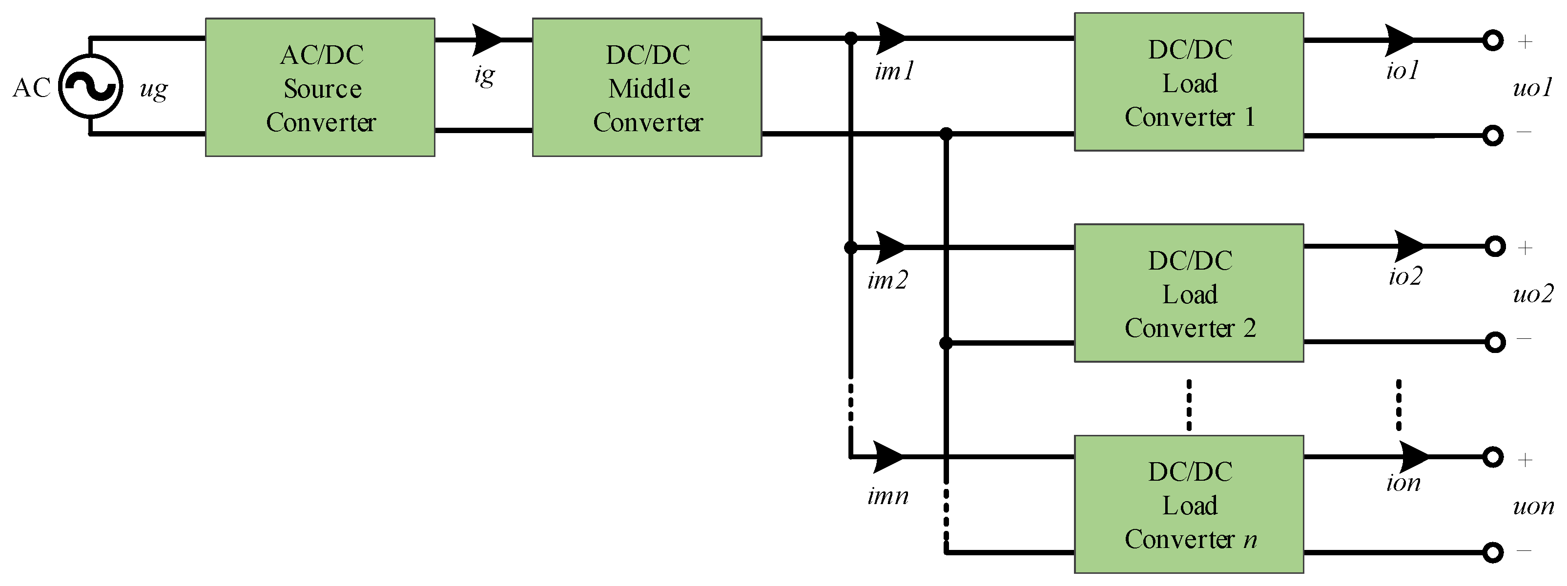
The power supply for multi-electrode arc welding is a multi-output current power system. Studies have been conducted on multi-output current power supplies, whereas there has been extensive research performed on multi-output voltage power supplies. Therefore, the power structure of the multi-output voltage power supply can be used as guidance to design the multi-output current power supply. The architecture of the multi-output voltage power source is shown in Figure 1, which is referred to as the intermediate bus type. The power supply in this architecture has a high overall efficiency, and its volume and cost are low. Thus, this architecture is a suitable multi-output power supply architecture.
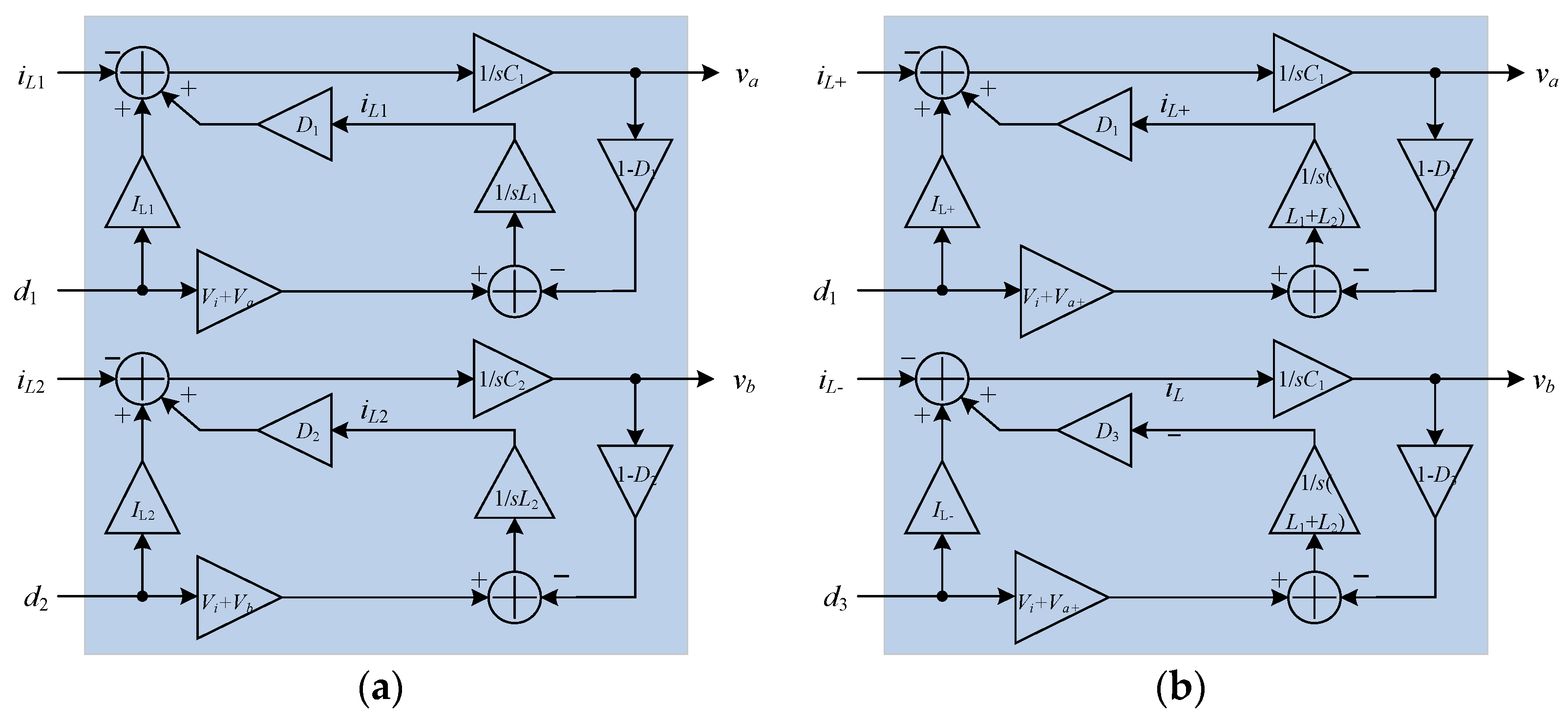
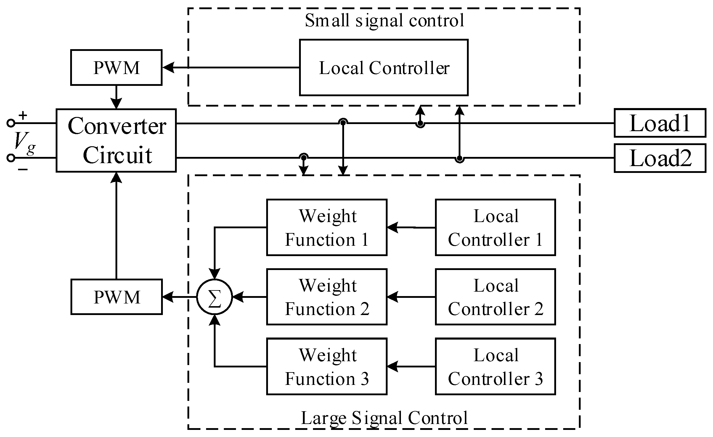
The control strategy of the multi-electrode arc welding power supply is the most important aspect of realizing multi-electrode welding. During the welding process, according to the welding process requirements, the current will be in a stable state or change rapidly at a certain time. The current change can be sorted into large-signal process and small-signal process according to different welding processes. In the large-signal process, the current changes over a large range, whereas in the small-signal process, it is dynamically adjusted within a small range. Therefore, the large- and small-signal modeling should be established before the control strategy is designed.
There are numerous small-signal modeling methods and many control methods based on the small-signal model. For example, the PID control method is based on the small-signal model. Ang et al. [7] studied the small-signal model of the PID controller based on the simulator for the DC-DC converter. This small-signal model describes the PID control process, but the model is not combined with the converter. The large-scale application of digital devices realizes the real-time tuning PID control method. On this basis, numerous researchers studied the adaptive PID control method [8,9], which can adjust the required duty cycle value in advance according to the established small-signal model. Based on the adaptive adjustment, Cao et al. [10] proposed the delay feedback automatic adjustment PID controller, which reduces the complexity of the control and shortens the PID controller’s intervention and adjustment times. However, it is not suitable for large-scale adjustment. To make the PID small-signal model suitable for large-scale regulation, Du et al. [11] proposed a PID controller based on the nonlinear small-signal model, which can complete the adjustment of some large signals but increases the complexity of the control system.
Small-signal control can only maintain stability at a steady operating point; however, the stability of the system under large-signal adjustment cannot be guaranteed, in which case the traditional linearized state space method is no longer applicable [12,13,14]. Therefore, it is necessary to establish a large signal model to determine the feasibility of the system.
Large-signal modeling methods are still under research. The traditional modeling method uses nonlinear switches to establish the large-signal model of the system [15]. However, this method is not suitable for the large signal model under different working conditions. The behavior description method is likewise used in large signal modeling. In addition, these two models are mostly used in simulation research [16]. Liu et al. [17] used the ideal transformer model to replace the switch to establish the large signal model; however, such a model can only be established in CCM (continuous conduction mode) mode. The traditional reduced-order simplified model substantially simplifies the system-level simulation and retains some module characteristics, which has evident advantages in simulation. However, this method cannot provide theoretical guidance to analyze the system [18]. Therefore, it is necessary to establish a new type of large signal model to describe the large signal change process in the welding process so as to apply the multi-electrode arc welding power supply.
Current multi-output welding power supplies involve combining multiple sources for different processes, using three or more electrodes with DC or AC current. This requires numerous power sources, increasing cost and impacting production efficiency. There is a need for a flexible, cost-effective multi-electrode power supply suitable for various processes. A power supply meeting the combination requirement can be achieved through multiple electrode combinations. Characterized by ease of use, affordability, and efficient control, this power supply holds significant potential. Research on multi-electrode arc welding power supplies is in its early stages, with no suitable method for the main circuit and control strategy.
In this study, we designed a topological structure for a multi-electrode arc welding power supply, dividing the current change process into large and small-signal change processes. By establishing models and analyzing the converter’s working principle, we designed a control method and constructed an experimental prototype. The resulting power supply offers improved response time and cost-effectiveness compared to traditional multi-output welding power supplies, increasing its applicability, response time, and cost-effectiveness as compared to conventional multi-output welding power supplies, therefore providing a viable option for broader applicability.

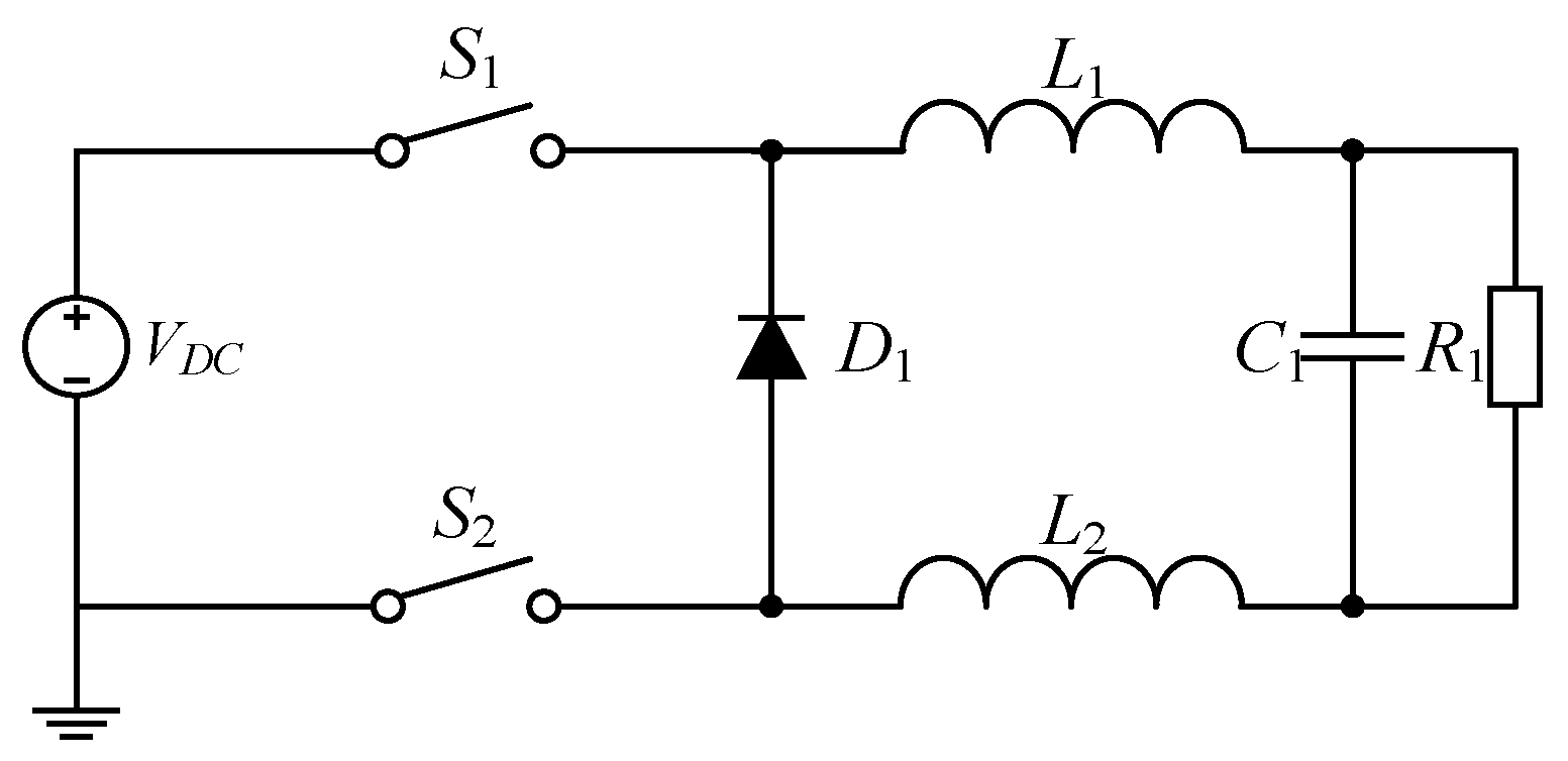
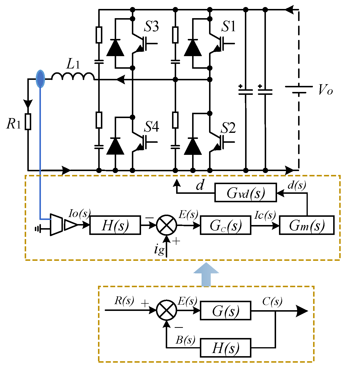
2. Topology of Multi-Output Arc Welding Power Supply

The multi-output arc welding power supply proposed in this study is shown in Figure 2. ig1 and ig2 are the target current values controlled by the controller; io1 and io2 are the actual values.
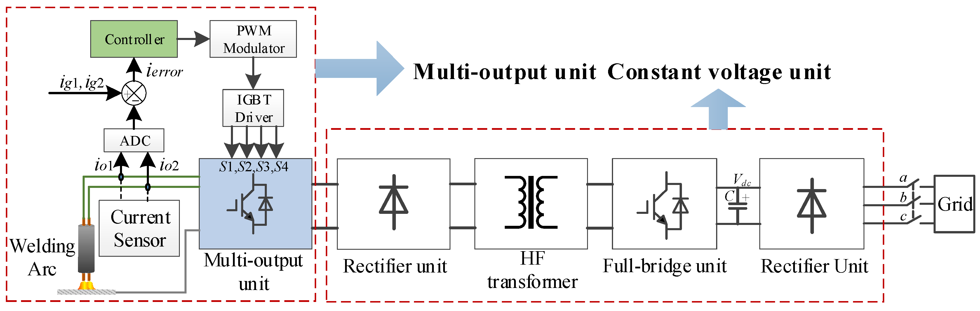
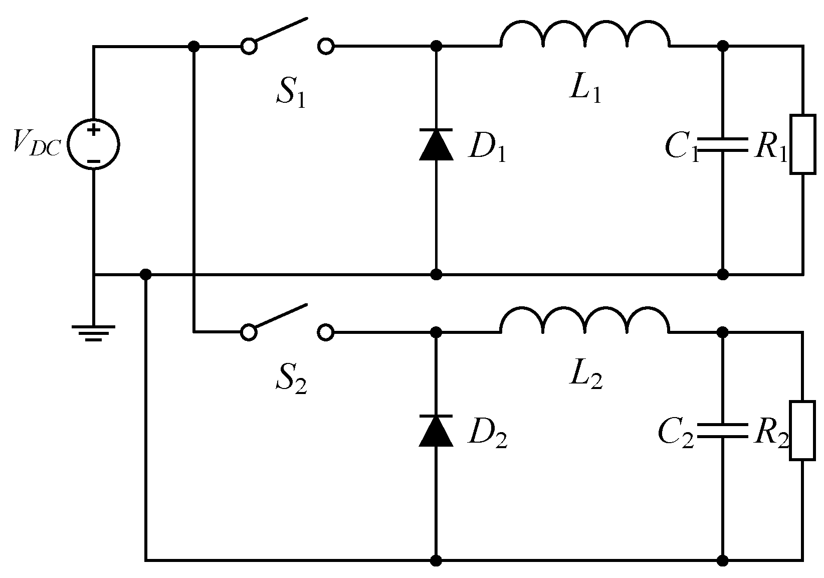
The converter includes a three-phase rectifier unit, a full-bridge inverter unit, a high-frequency transformer, a rectifier unit, and a multi-channel output unit. The three-phase rectifier unit converts the 380 VAC to 540 VDC, which is converted to a high-frequency pulse with a frequency of 20 kHz after passing through the full-bridge inverter unit. The turn ratio of the high-frequency transformer is 14:3. After passing through the transformer, the voltage of the high-frequency pulse decreases and the current rises. After the output rectifier unit, the voltage becomes 50 VDC. This voltage stays constant during welding and is not affected by current output; hence, it can be omitted from the analysis in this study.
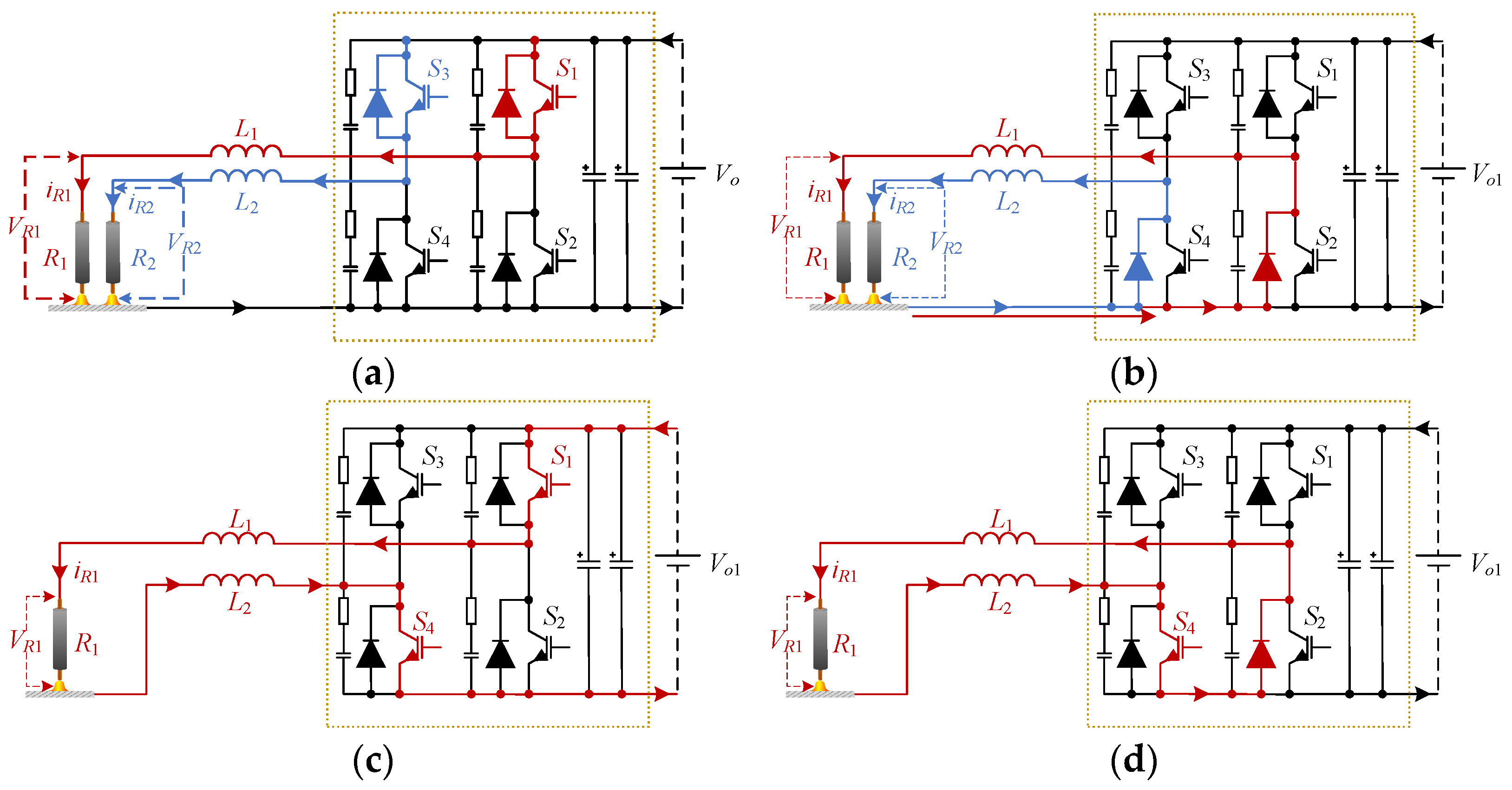
The multi-output unit is the most important component of the converter designed in this study, as shown in Figure 3. S1S4 are the IGBTs in the circuit; L1 and L2 are the inductors for stable current in the circuit; R1 and R2 represent the welding arcs. In the stable welding process, the welding current and voltage basically remain constant and only change within a small range. I arc can be regarded as the resistance to analysis. IR1, IR2, VR1, and VR2 are the welding currents and welding voltages, respectively.
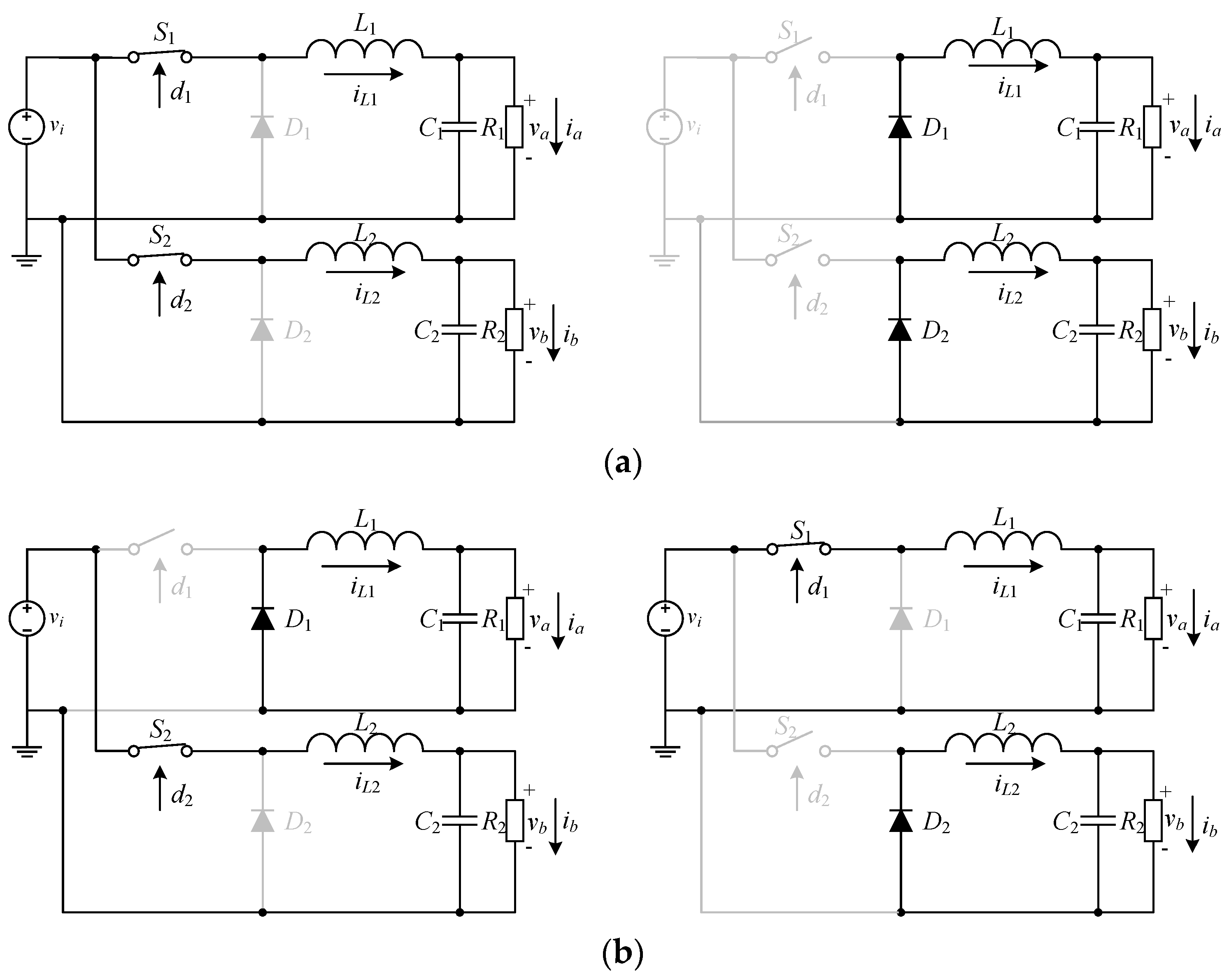
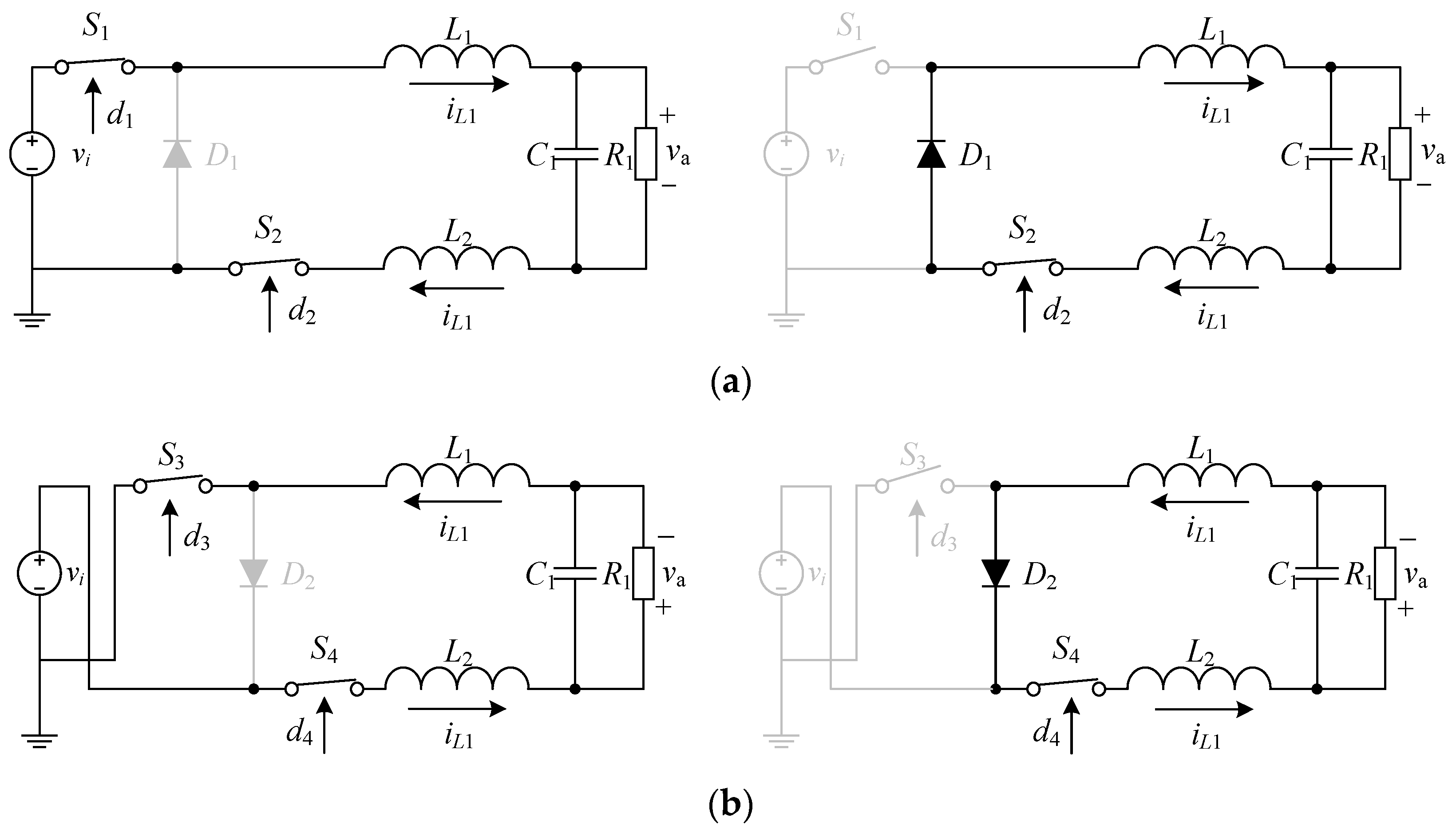
The multi-output unit is composed of the buck chopper circuit, and according to the different output, this circuit can be converted into a full-bridge inverter circuit. We use different colors to represent different output patterns: In Figure 3a, the red and blue lines represent two DC currents; in Figure 3b, the red and blue lines represent different current directions in AC mode. 
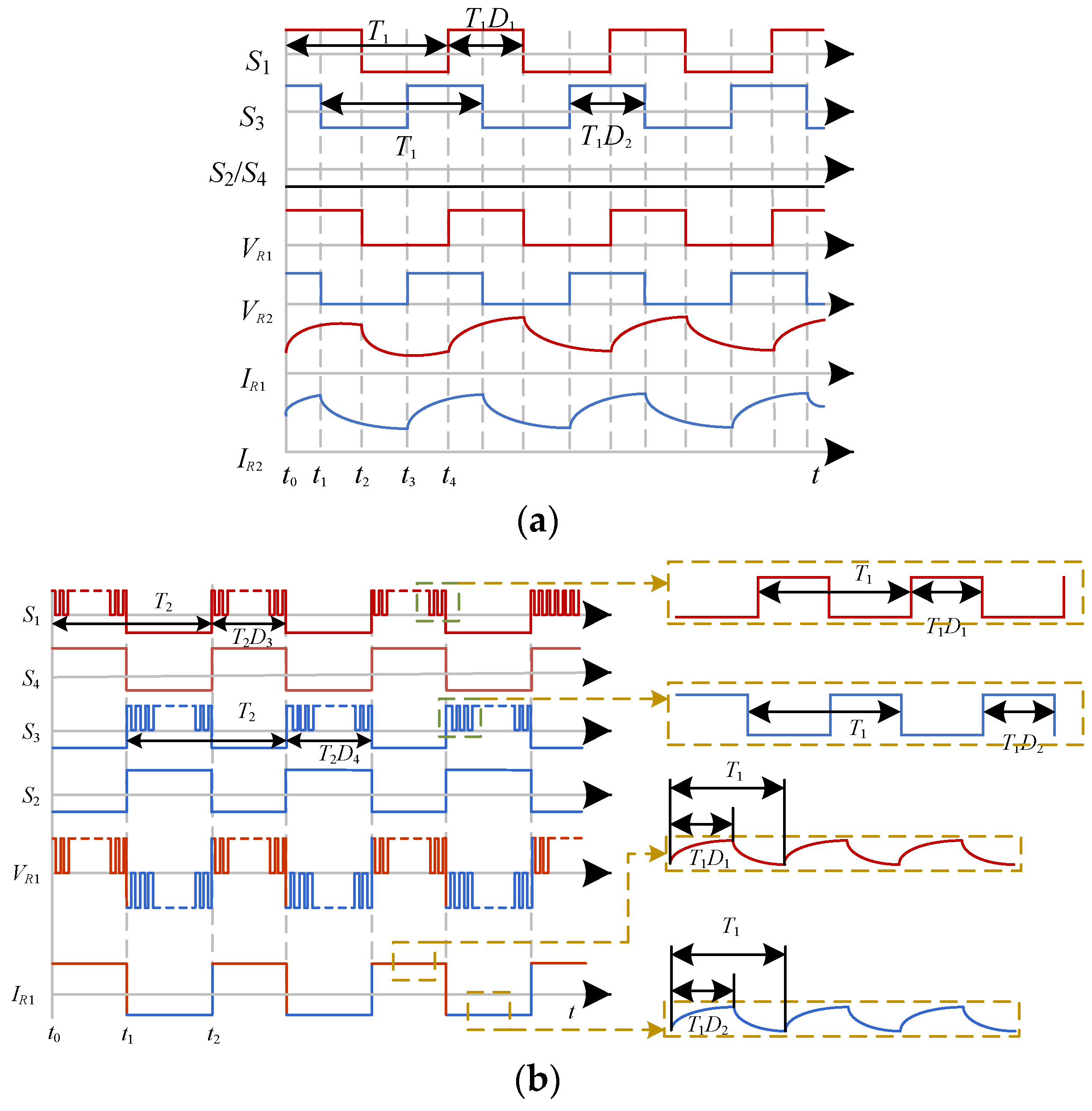
Figure 4 illustrates the working principle of the IGBT in each mode, and the color representation is the same as in Figure 3. The multi-output unit can output dual DC or single AC, depending on the requirement.
In the welding process, an inductor is used in the converter to maintain a stable current, and its operation mode is always CCM mode. Therefore, during the welding period, the output current and voltage remain constant. In the analysis, the welding arc is regarded as a resistance, whose magnitude changes slightly within a certain range.
As shown in Figure 4, S1, S2, S3, and S4 present the drive waveform of each IGBT. VR1 and VR2 are the voltages of the welding arc. IR1 and IR2 are the currents of the welding arc. S2 and S4 are keep in turn off state. When S1 and S3 are switched on, the currents flow through the IGBTs as shown in Figure 3a, and when S1 and S3 are switched off, the currents flow through the internal diode in S2 and S4 as shown in Figure 3b. So, in DC mode, when S1 and S3 are switched on and off, the DC voltage is chopped, inductors L1 and L2 are in CCM mode, and the current through the resistance is DC current. This working principle is shown in Figure 3a,b, and the specific waveform is shown in Figure 4a,b. In Figure 4a,b, T1 = 50 μs, D1 and D2 are the duty cycles of the driving waveform of the IGBT. The duty cycles are changed according to the setting current.
At time T0, S1 and S3 are switched off; the current on resistor R1 flows from Vo1+ through S1, L1, and R1 to Vo1−, and the current on resistor R2 flows from voltage Vo1+ through S2, L2, and R2 to Vo1−. At this time, inductors L1 and L2 store energy, and the current continues to increase.
At time T1, S1 is switched on and S3 is switched off; the inductor L1 continues to store energy, and the current on R1 continues to increase. Since S3 is off, L2 discharges to stop current changes, and the current flowing through R2 decreases. At this time, the current loop flowing through R2 passes through the internal reverse diodes of S4, R2, and L2.
At time T2, S1 and S3 are switched off. The energy stored in the inductor L1 starts discharging, and the energy in the inductor L2 continues to discharge to maintain the current flowing across the resistors R1 and R2. At this time, the current loop flowing through R1 passes through the internal reverse diodes of S2, R1, and L1.
At time T3, S3 is switched on, S1 is switched off, inductor L2 is charged, and the current flowing through resistor R2 starts to increase. At this point, the current across resistor R1 continues to decrease.
At time T4, S1 and S3 are switched on, returning to time T0, as described above.
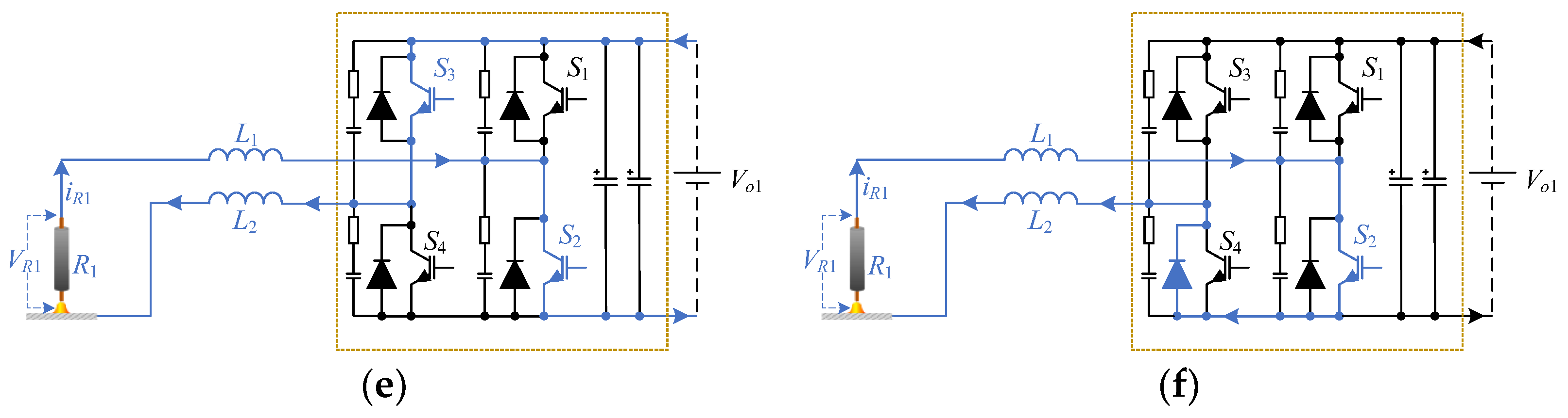
As shown in Figure 4b, S1, S2, S3, and S4 present the drive waveform of each IGBT. VR1 is the voltage of the welding arc. IR1 is the current of the welding arc. When the converter is in AC mode, the welding power supply can output forward and reverse currents. In the welding process, the frequency of AC current is generally 40~50 Hz. Therefore, in AC mode, an AC cycle can be regarded as the combination of two DC modes, which are the forward and reverse DC modes, respectively. Another difference with DC mode is that when the S1 or S3 is switched on or off, the S2 or S4 are kept in the on or off state to provide the circuit with continuous current. The specific working waveform is shown in Figure 4b, where T2 is the cycle of AC welding and D3 and D4 are the forward and reverse current duty cycles during AC welding, respectively. In contrast with the DC mode, in the inductor discharge stage, assume that the loop controlled by S1 and S4 is the forward current as shown in Figure 3c, and the loop controlled by S2 and S3 is the reverse current as shown in Figure 3e. When the converter works in forward AC mode, S1 is switched on or off. In this mode, S4 is kept in turn-on mode, while S2 and S3 are kept in turn off states, and the continuous current can flow through S4 and the internal diode in S2 as shown in Figure 3d. When the converter works in reverse AC mode, S3 is switched on or off. In this mode, S2 is kept in turn-on mode, while S1 and S4 are kept in turn-off states, and the continuous current can flow through S2 and the internal diode in S4 as shown in Figure 3f. The discharge loop in the forward current is through L1, R1, L2, S4, and internal reverse diodes in S2. The discharge circuit for the reverse current is through internal reverse diodes of S4, R1, L1, S2, and L2.
At time T0, S1 and S4 are switched on simultaneously, and the current flows through Vo1+, S1, R1, and S4 to Vo1−. During the AC forward period, S1 is switched off and on at a frequency of 20 kHz, while S4 is always on. Therefore, this mode can be considered to be the same as the DC mode, where one IGBT is used for chopping while the other switch in the loop is always on.
At time T1, in AC mode, the current changes from forward to reverse, and S1 and S4 are switched off. Then, after a certain dead time, S2 and S3 are switched on. The current flows through Vo1+, S3, R1, and S2 to Vo1−. In the AC reverse mode, S3 is switched off and on at a frequency of 20 kHz, and S2 is consistently on. The mode in this case can be regarded as the reverse DC mode.
At time T2, S2 and S3 are switched on, and S1 and S4 are switched off, as at time T0. At this time, a complete AC cycle has been completed.
In AC mode, the dead time should be considered. For the converter in this paper, there is no dead time in DC mode. In AC mode, there is dead time when the forward and reverse currents are switched. In this paper, the difference with the full-bridge inverter is that there is no secondary side of the transformer to provide a continuous flow circuit to release the energy of the primary side when switching. Therefore, when the voltage on the inductor and welding arc drops to the constant voltage, the internal diode of the opposite IGBT would be turned off by a hard switch. Since the constant voltage is 50 V, the voltage on the IGBT is relatively low, and the effect on the IGBT is small due to the protection of the RC absorption circuit and the high voltage tolerance of the IGBT module. Due to inertia, the change in the arc lags behind the change in the current, so when the current drops to zero, the arc does not disappear.

3. Modeling

3.1. Small-Signal Modeling

There are numerous small-signal modeling methods, such as the state-space averaging method [12], the time averaging method [13,14], and the description function method [15]. In this study, a small-signal model of a multi-electrode arc welding power source is established based on the time averaging method. According to the time-average equivalent circuit principle [14], the small-signal equivalent circuit of the multi-electrode arc welding power supply can be obtained, as shown in Figure 5.
Taking the output loop controlled by S1 as an example, the following switching states can be obtained:
Switching state 1: S1 is switched on, diode D1 is switched off; the inductor L1 and capacitor C1 are charged by the input power supply, and power is distributed to the load R1. The inductor current iL1 rises linearly with slope e1. Let the state variable x = [iL1 va]T, then the equation of state is:
i · L 1 = v a / L 1 + v i / L 1 v · a = i L 1 / C 1 v a / ( R 1 C 1 )
Switch state 2: switch S1 is switched off, diode D1 is switched on, inductor L1 discharges to load R1 and capacitor C1, and inductor current iL1 linearly decreases with slope −e2, then the state equation is:
i · L 1 = 1 L 1 v a v · a = 1 R 1 C 1 v a
The rising slope e1 and falling slope e2 of inductor current are respectively:
e 1 = ( v i v a ) / L 1 e 2 = v a / L 1
Additionally, since the two groups of parallel chopper circuits have the same structure and device parameters, the state equations of the control loop of S2 can be obtained as follows:
i · L 2 = v b / L 2 + v i / L 2 v · b = i L 2 / C 2 v b / ( R 2 C 2 )
i · L 2 = 1 L 2 v b v · b = 1 R 2 C 2 v b
The rising slope e3 and falling slope e4 of inductor current are, respectively:
e 3 = ( v i v b ) / L 2 e 4 = v b / L 2
According to the converter principle introduced in Figure 3, when the converter outputs two DC currents, the current is controlled by regulating the duty cycle of the S1 and S2 driving voltages. According to the different current values of IA and IB, the converter can be divided into four states, as shown below:
Thus, combining Figure 6 with Equations (1)–(6), letting the state variable x = [iL1 va iL2 vb]T, the model of the converter in DC mode can be obtained by using the state space average method:
x ¯ · = A x ¯ + B v i
Among them,
A = 0 1 L 1 ( 1 d 1 ) 0 0 1 C 1 d 1 1 R 1 C 1 0 0 0 0 0 1 L 2 ( 1 d 2 ) 0 0 1 C 2 d 2 1 R 2 C 2
B = 1 L 1 d 1 0 1 L 2 d 2 0 T
When the converter outputs AC, the simplified model is shown as Figure 7,
By analyzing the working mode in the AC mode, the following switch states can be obtained:
Switching state 1: S1 and S2 are switched on, diode D1 is switched off, the inductor L1 and capacitor C1 are charged by the input power supply, and output power is sent to the load R1. The inductor current iL1 rises linearly with slope e1. Let the state variable x = [iL1 va]T, then the equation of the state is:
i · L 1 = v a / ( L 1 + L 2 ) + v i / ( L 1 + L 2 ) v · a = i L 1 / C 1 v a / ( R 1 C 1 )
Switch state 2: S1 is switched off, diode D1 is switched on; inductor L1 discharges to load R1 and capacitor C1, and inductor current iL1 decreases linearly with slope −e2, then the state equation is as follows:
i · L 1 = 1 L 1 + L 2 v a v · a = 1 R 1 C 1 v a
The rising slope e1 and falling slope e2 of the inductor current are:
e 1 = ( v i v a ) / ( L 1 + L 2 ) e 2 = v a / ( L 1 + L 2 )
In the AC state, the converter can be divided into four states, as shown below:
Therefore, combining Figure 8 and Equations (10)–(12), the state variable x = [iL1+ va+ iL1− va]T, the state space averaging model of the converter in AC mode can be obtained as follows:
x ¯ · = A x ¯ + B v i
Among them:
A = 0 1 L 1 + L 2 ( 1 d 1 ) 0 0 1 C 1 d 1 1 R 1 C 1 0 0 0 0 0 1 L 1 + L 2 ( 1 d 3 ) 0 0 1 C 1 d 3 1 R 1 C 1
B = 1 L 1 + L 2 d 1 0 1 L 1 + L 2 d 3 0 T
Small-signal disturbances are applied to the state space average model as shown in Equations (8), (9), (13) and (14), namely:
i L 1 = I L 1 + i L 1 ^ , i L 2 = I L 2 + i L 2 ^ v a = V a + v a ^ , v b = V b + v b ^ d 1 = D 1 + d 1 ^ , d 2 = D 2 + d 2 ^ , d 3 = D 3 + d 3 ^ , d 4 = D 4 + d 4 ^
In this form, IL1, IL2, Va, Vb, D1, D2, D3, and D4 are the steady values, and the “^” symbol variable is the small-signal disturbance.
Therefore, the expression of the small-signal model in the DC mode is as follows:
i ^ L 1 = 1 s L 1 [ ( 1 D 1 ) v ^ a + ( V a + V i ) d ^ 1 + D 1 v ^ i ] v ^ a = 1 s C 1 ( D 1 i ^ L 1 + I L 1 d ^ 1 i ^ L 1 ) i ^ L 1 = 1 s L 2 [ ( 1 D 2 ) v ^ b + ( V b + V i ) d ^ 2 + D 2 v ^ i ] v ^ b = 1 s C 2 ( D 2 i ^ L 2 + I L 2 d ^ 2 i ^ L 2 )
The expression of the small-signal model of the AC mode is as follows:
i ^ L + = 1 s ( L 1 + L 2 ) [ ( 1 D 1 ) v ^ a + + ( V a + + V i ) d ^ 1 + D 1 v ^ i ] v ^ a + = 1 s C 1 ( D 1 i ^ L + + I L + d ^ 1 i ^ L + ) i ^ L = 1 s ( L 1 + L 2 ) [ ( 1 D 3 ) v ^ a + ( V a + V i ) d ^ 3 + D 3 v ^ i ] v ^ a = 1 s C 1 ( D 3 i ^ L + I L d ^ 3 i ^ L )
According to the small-signal model of the converter shown in Equations (16) and (17), the small-signal model of the converter shown in Figure 9 can be obtained when the input voltage disturbance is ignored.
After obtaining the transfer function of the equivalent circuit, the equivalent small-signal block diagram of the converter can be determined, as shown in Figure 10. Herein, G(s) is the transfer function between duty cycle D(s) and output Io(s), and E(s) is the error transfer function between Io(s) and Ig. Gm(s) is the transfer function of the PWM generator, H(s) is the transfer function of the sampling, and Gvd(S) is the transfer function of the controller.
The final small-signal model is as follows:
G D C ( s ) = G c ( s ) U o d 1 1 1 + s L 1 R 1 + S 2 L 1 C 1
G A C ( s ) = G c ( s ) U o d 1 1 1 + s L 1 + L 2 R 1 + S 2 ( L 1 + L 2 ) C 1

3.2. Large Signal Modeling

Since the small-signal working state is a response to the small-signal disturbance, when the power supply output changes rapidly, it will be in the large-signal working state, and a large-signal model is necessary to describe the transformation process of the converter [18,19,20]. During the large-signal process, the welding current changes rapidly, and the current control strategy must be fast and accurate to ensure that the current can be adjusted to the given value. In this section, we establish a large signal model to describe the working state of the converter in the large signal process. According to the small-signal establishment process described in Section 3.1, the averaged global state space model can be generally described as follows:
x · = A ( x , u ) x + B ( x , u ) u y = C ( x , u ) x + D ( x , u ) u
where x is the system state variable; U is the input variable; Y is the output variable; A, B, C, and D are the system matrixes of the response. According to the working principle of the converter mentioned above, the converter for welding processes is a non-linear system; if using the same large-signal control strategy for all large current changes, the current response time would be different. Therefore, the large-signal working phase should be divided into n sub-phases.
x · = i = 1 n w i ( X i , U i ) [ A i ( X i , U i ) x + B ( X i , U i ) u ] y = i = 1 n w i ( X i , U i ) [ C i ( X i , U i ) x + D ( X i , U i ) u ]
Among them, Xi and Ui are the state and input variables of the model, respectively; Wi is the weight function corresponding to the local model, which can be a Gaussian function [21], a trigonometric function [22], an exponential function [23,24,25], etc., due to the requirements.
0 w i ( X i , U i ) 1 i = 1 n w i ( X i , U i ) = 1
Because the output current range of the converter is large, an individual weight function cannot cover the entire working range, so the global working area of the converter is divided into three local working areas according to the actual working conditions of the converter.
Thus, the large-signal model of each sub-phase is obtained, after which the weight function is designed, finally yielding the global model. After the welding arc is generated, the voltammetry characteristics of the current and voltage are specific. For example, in the TIG welding process, the voltammetry characteristics are U = 10 + 0.04i. When the current changes, the voltage changes along with it. As shown in Figure 11, the current is limited to 300 A, and the work phase is divided into three segments, namely, 0–100, 101–200, and 201–300 A. Therefore, the benchmark operating points of the large signal are (14, 100), (18, 200), and (22, 300), respectively. In different working periods, the coefficients of the weight function are different, and the function of the large signal changes accordingly.
Considering the complexity and accuracy, the Gaussian function is selected as the weight function:
w i ( x ) = μ i ( x ) j = 1 r μ j ( x )
where
μ i ( x 1 , x 2 ) = i = 1 3 ( 1 1 / exp [ m i ( x i x i 0 b ) ] 1 + exp [ m i ( x i x i 0 b ) ] )
where mi, xi0 and b are constant terms.
When the input voltage and load current changes are considered separately, the weight function can be designed as follows:
μ i ( i g ) = 1 1 / exp [ m i g ( i g i g 0 i a ) ] 1 + exp [ m i g ( i g i g 0 i a ) ] μ j ( i l o a d ) = 1 1 / exp [ m i l o a d ( i l o a d i l o a d 0 j b ) ] 1 + exp [ m i l o a d ( i l o a d i l o a d 0 j b ) ]
wherein
m i g 0 = 13 Δ i g 0 ; a = Δ i g 0 2 ; m i l o a d 0 = 13 Δ i l o a d 0 ; b = Δ i l o a d 0 2
Therefore, the large signal model of the converter can be approximated as:
G v d ( s ) = w 1 ( x ) G v d 01 ( 1 + s / w z ) 1 + s / w p 1 + 2 3 [ w i ( x ) 1 1 + s L / R + s 2 L C ]

4. Control Strategy Design

The above analysis shows the small-signal and large-signal models of the multi-output power supply; based on these models, the adaptive control strategy of the converter system can be constructed, as shown in Figure 12. After the load current is measured, we can determine whether the power supply is in the small-signal or the large-signal work process. If it is in the small-signal work process, then we adopt the small-signal control strategy. If it is in the large-signal work process, different weight functions must be selected according to the current value. The transfer function of the output to the control signal is as follows:
v c t r l i o = i = 1 n w i ( I g , i l o a d ) G c i ( I g , i l o a d )
According to Equation (28), the controller can be described as follows: when the working conditions of the converter (Ig and iload) in a large range of current change, the weight function would monitor the change of working state in real-time and be adaptive to adjust the action of each local controller weight coefficient to ensure the system has good global control performance of the work area and a good transient response.
Therefore, during the welding process, the method proposed in this paper can be divided into large signal processing and small signal processing. The limitation of traditional PID control methods is that the PID adjusts using the same Kp and Ki parameters for all current modulations, which results in inconsistent results for small and large currents. Therefore, in this research, the current is divided into three ranges and combined with different weight functions and PIDs in each range, thus the adjustment effect is consistent in different current ranges. Based on the above theory, when the current is switched from a small to a large value, the weight function will be switched first so that the current will quickly rise to the required value.

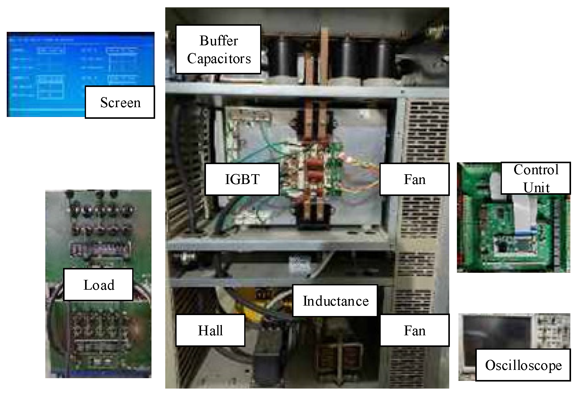
5. Experimental Verification

To testify to the above theoretical analysis, an experimental prototype is built; the experimental prototype is shown in Figure 13. The HMI for multi-electrode output is designed, and the current and voltage can be set by the touch screen. STM32F407 is used as the controller to output the PWM to control the multi-channel output unit. The load box is used to simulate the arc, and the resistance of the load box ranges from 0.05 to 4 Ω. The bus capacitor is placed behind the constant-voltage output unit to stabilize the voltage during welding. A total of six 2200 uF electrolytic capacitors are used.
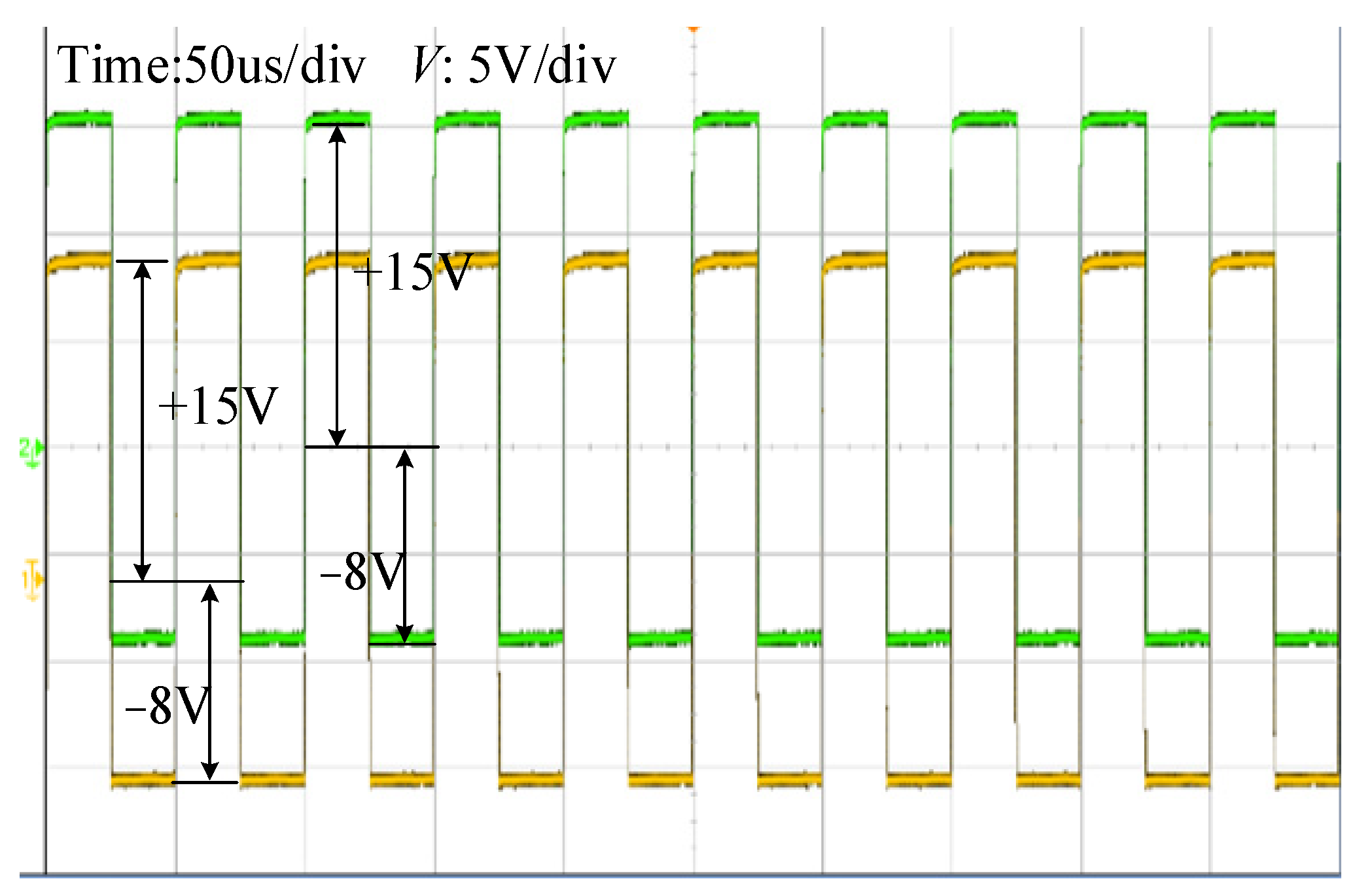
In order to prevent the IGBT from being misdirected by dv/dt when the IGBT is turned off, a reverse turn-off voltage is applied to the IGBT in the drive circuit. The IGBT drive circuit designed in this paper has a +15 V/−8 V drive waveform, as shown in Figure 14.
The rapid change of current will produce high voltage at both ends of the IGBT, so it is necessary to set up a protection circuit to protect the IGBT and to choose IGBTs with a high withstand voltage as well. In the circuit, the IGBT modules with a high withstand voltage value of 1200 V are selected. Moreover, an RC circuit is connected in parallel with the drain and source of the IGBT to absorb the peak voltage caused by the fast shutdown. The RC absorption circuit in this paper has a resistance of 6.2 ohms and a capacitor of 10 nF.
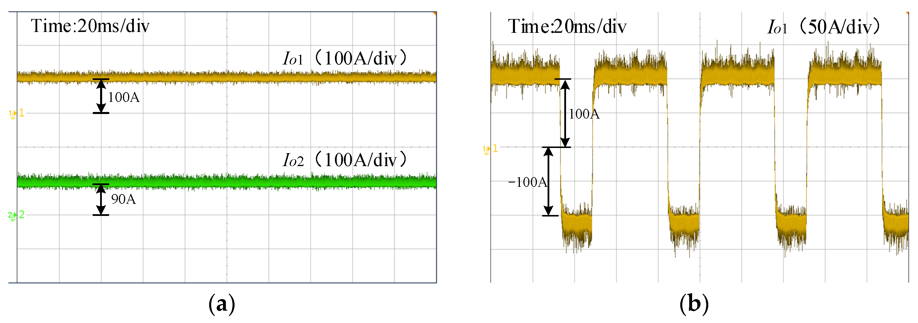
Experiments are designed to verify the performance of the converter. First, the experiment is conducted to check the current output of the converter in DC mode and AC mode. In DC mode, the converter could generate two current outputs of different values. In AC mode, the converter could output the same forward and reverse currents. In addition, in AC mode, the times for forward current and reverse current are 21 ms and 4 ms, respectively.
The small-signal model and the large-signal model are also testified to. To verify the performance of the control strategy, the adjustment time could be observed and compared with the traditional PID closed-loop control strategy.
The experimental waveform in steady state is shown in Figure 15a,b indicate that the output current in DC or AC is relatively stable and the inductor is working in CCM mode. In steady-state operation, the output current is stable, indicating satisfactory system stability.
In the working state of the small-signal process, the duty cycle change will not be drastic. When the input voltage changes drastically, it can be quickly adjusted to the given current. As shown in 
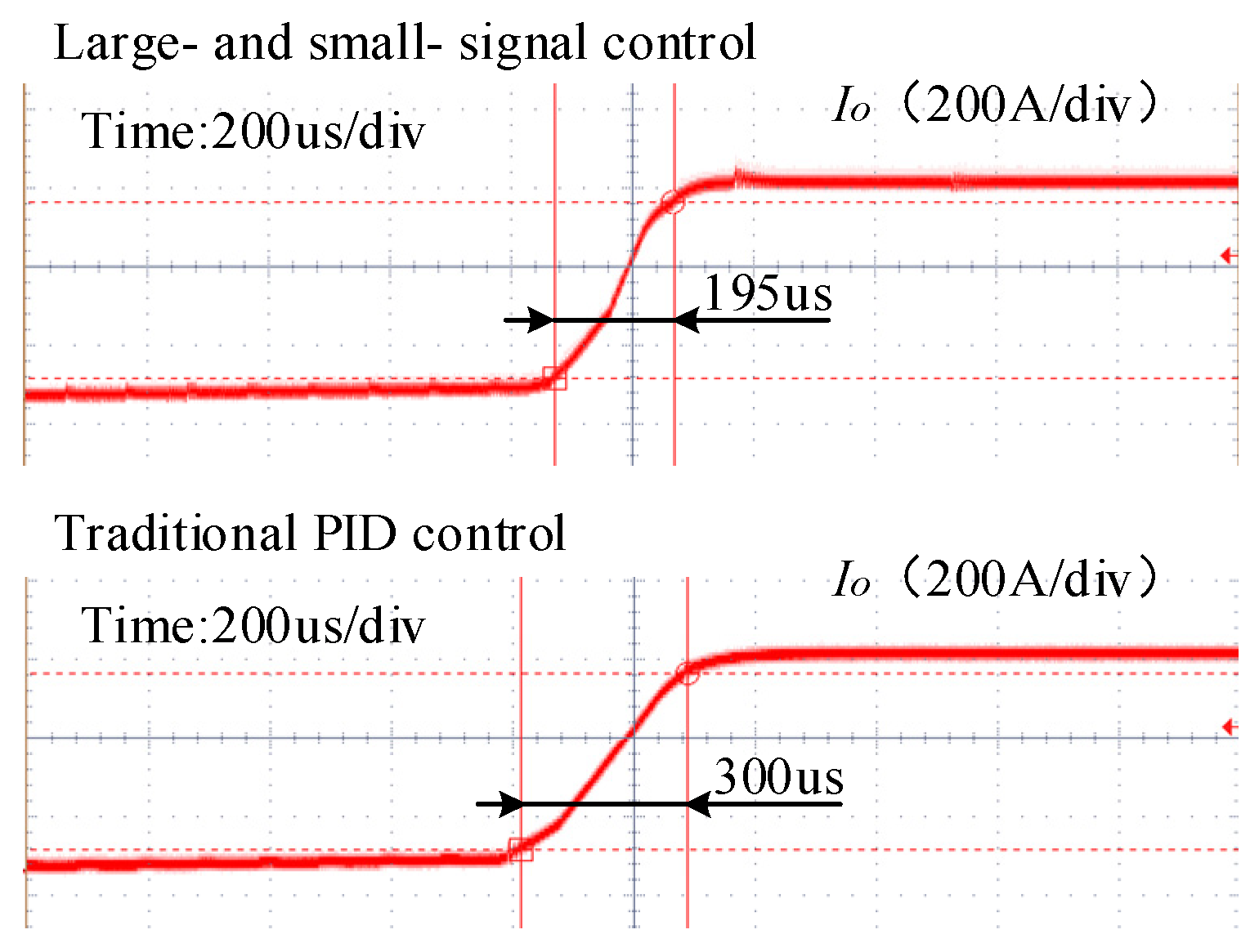
Figure 16, compared with the traditional control system with PI regulation only, the current system changes steadily and adjusts quickly. During welding, the stable current can keep the welding arc stable.
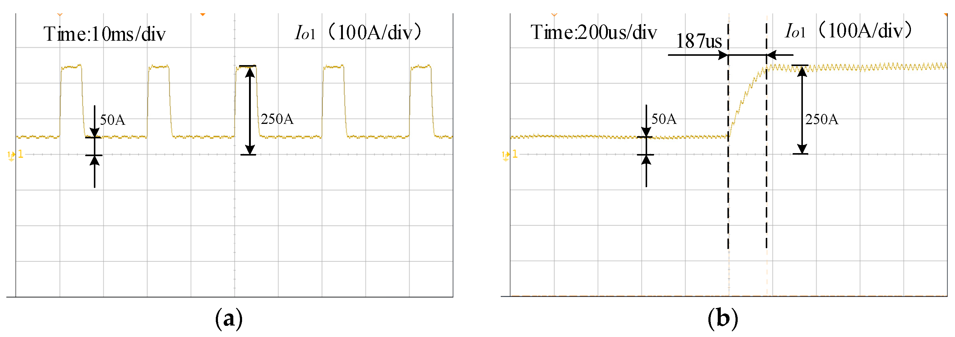
By observing the conversion between large current and small current, it can be seen that the large-signal control strategy designed in this paper can realize fast adjustment. As shown in 
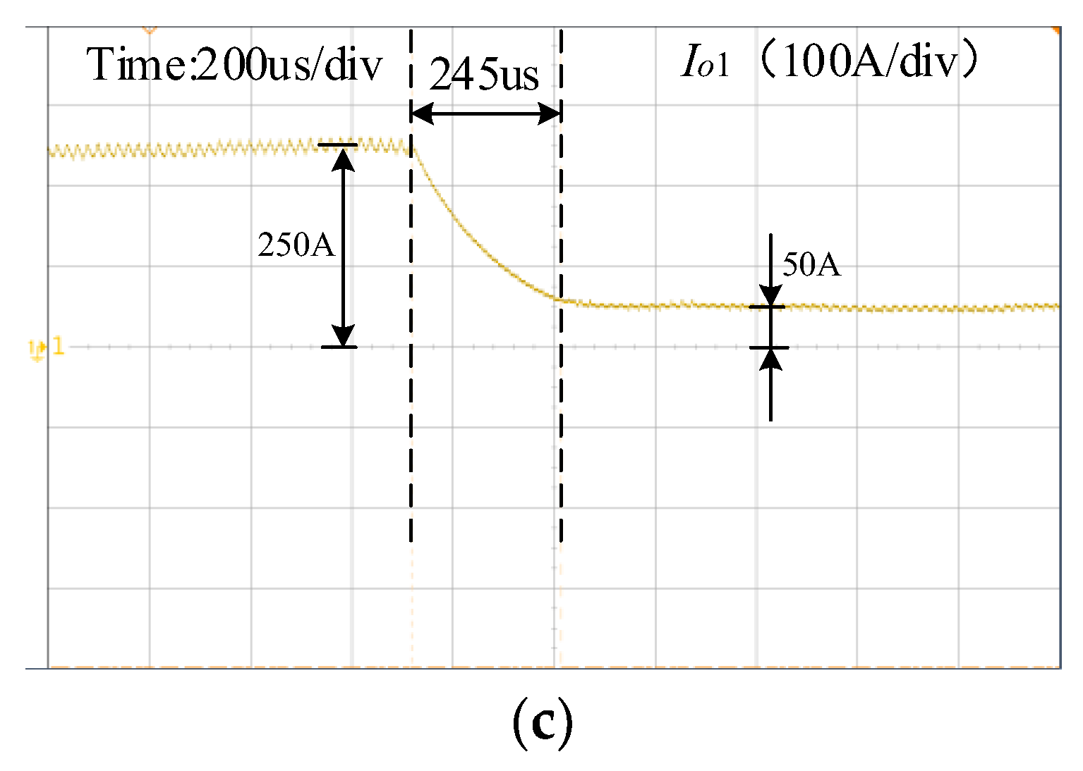
Figure 17, only 187 us are taken when the current rises from 50 A to 250 A, and only 245 us are taken when the current falls from 250 A to 50 A. The response time is short, and the system has a small overshoot.
In the welding process, the large signal generally also appears when the current changes significantly. Therefore, the current direction change in the AC state is the most typical application scenario. As shown in 
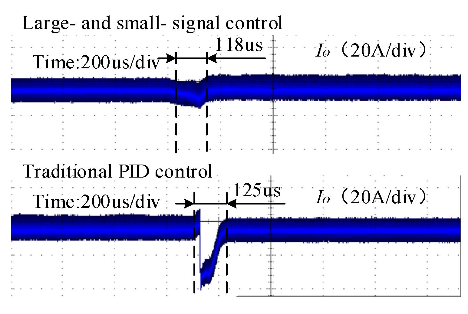
Figure 18, compared with the traditional PID, the current changes faster in the AC state, and a higher welding frequency can be achieved in AC welding.

6. Conclusions

In this paper, based on the intermediate bus power architecture, we designed a converter suitable for the multi-output arc welding power supply and introduced its topology. Based on the designed topology, different IGBTs can be controlled to realize dual DC current output or single AC current output. When two IGBTs are controlled to switch on or off, the converter can generate dual DC current output. When an IGBT is controlled to switch on or off or to stay in the on state, the converter can output AC current. The working principle of the converter is analyzed in this paper and can be easily applied in a converter.
The small-signal model of the converter in DC and AC modes and the large-signal model of the system are established. The small-signal model is based on the time-averaging method, while the large-signal model is based on geometric segmentation. Based on the established small- and large-signal models, different current changes would be controlled by different control strategies to realize the rapid current adjustment.
An experimental prototype was designed to verify the model we proposed. The results showed that the converter designed in this study has good stability, and the control strategy can rapidly respond and generate the output current compared with the traditional PID control in both small-signal adjust and large-signal adjust, such that the welding current and adjustment ability are significantly improved. Furthermore, the proposed converter shows the availability of higher-frequency welding.
For future work, the research on multi-output power supplies for multi-electrode arc welding will focus on improving the current response speed and current output synchronization at high speeds to achieve higher AC current frequencies, as well as continuing to advance the control method of multi-output power supplies.

Author Contributions

Conceptualization, S.C.; Methodology, Y.Y.; Validation, M.L.; Writing—original draft, J.Z.; Funding acquisition, H.Z. All authors have read and agreed to the published version of the manuscript.

Funding

This research was funded by the National Natural Science Foundation of China under grant number 52205325.

Data Availability Statement

The data presented in this study are available in article.

Conflicts of Interest

The authors declare no conflict of interest.

References

  1. Chen, S.; Feng, L.; Li, L.; Yin, S.; Zhang, S. Principle and parameter design of arc welding inverter using soft switching technique. China Weld. 1998, 1, 63–70. [Google Scholar]
  2. Chen, J.S.; Lu, Y.; Li, X.R.; Zhang, Y.M. Gas tungsten arc welding using an arcing wire. Weld. J. 2012, 91, 261–269. [Google Scholar]
  3. Chen, S.J.; Zhang, L.; Wang, X.P.; Wang, J. Stability of the cross-arc process—A preliminary study. Weld. J. 2015, 94, 158–168. [Google Scholar]
  4. Lee, D.Y.; Leifsson, L.; Kim, J.; Lee, S.H. Optimization of hybrid tandem metal active gas welding using Gaussian process regression. Sci. Technol. Weld. Join. 2020, 25, 208–217. [Google Scholar] [CrossRef]
  5. Zhang, Y.; Zhang, S.; Jiang, M.; Wu, L. Keyhole double-sided arc welding process. J. Mater. Sci. Technol. 2001, 17, 159–160. [Google Scholar] [CrossRef]
  6. Li, K.H.; Chen, J.S.; Zhang, Y. Double-electrode GMAW process and control. Weld. J. 2007, 86, 231. [Google Scholar]
  7. Ang, K.H.; Chong, G.; Li, Y. PID control system analysis, design, and technology. IEEE Trans. Control Syst. Technol. 2005, 13, 559–576. [Google Scholar]
  8. Arias, M.; Diaz, M.F.; Lamar, D.G.; Linera, F.M.; Sebastian, J. Small-signal and large-signal analysis of the two-transformer asymmetrical half-bridge converter operating in continuous conduction mode. IEEE Trans. Power Electron. 2014, 29, 3547–3562. [Google Scholar] [CrossRef] [Green Version]
  9. Bahrami, H.; Sepehrian, H.; Park, C.S.; Rusch, L.A.; Shi, W. Time-domain large-signal modeling of traveling-wave modulators on SOI. J. Light. Technol. 2016, 34, 2812–2823. [Google Scholar] [CrossRef] [Green Version]
  10. Cao, S.G.; Rees, N.W.; Feng, G. Quadratic stability analysis and design of continuous-time fuzzy control systems. Int. J. Syst. Sci. 1996, 27, 193–203. [Google Scholar] [CrossRef]
  11. Du, X.; Helaoui, M.; Jarndal, A.; Liu, T.; Hu, B.; Hu, X.; Ghannouchi, F.M. ANN-based large-signal model of AlGaN/GaN HEMTs with accurate buffer-related trapping effects characterization. IEEE Trans. Microw. Theory Tech. 2020, 68, 3090–3099. [Google Scholar] [CrossRef]
  12. Zurbriggen, I.G.; Ordonez, M.; Anun, M. PWM-geometric modeling and centric control of basic DC-DC topologies for sleek and reliable large-signal response. IEEE Trans. Ind. Electron. 2015, 62, 2297–2308. [Google Scholar] [CrossRef]
  13. Gregorcic, G.; Lightbody, G. Local model network identification with Gaussian processes. IEEE Trans. Neural Netw. 2007, 18, 1404–1423. [Google Scholar] [CrossRef]
  14. Iqbal, M.T.; Maswood, A.I. An explicit discrete-time large- and small-signal modeling of the dual active bridge DC–DC converter based on the time scale methodology. IEEE Trans. Emerg. Sel. Ind. Electron. 2021, 2, 545–555. [Google Scholar] [CrossRef]
  15. Kapat, S.; Krein, P.T. A tutorial and review discussion of modulation, control and tuning of high-performance DC-DC converters based on small-signal and large-signal approaches. IEEE Open. J. Power Electron. 2020, 1, 339–371. [Google Scholar] [CrossRef]
  16. Li, C.; Du, Z. A novel method for computing small-signal stability boundaries of large-scale power systems. IEEE Trans. Power Syst. 2013, 28, 877–883. [Google Scholar] [CrossRef]
  17. Liu, S.; Zhou, L.; Lu, W. Simple analytical approach to predict large-signal stability region of a closed-loop boost DC–DC converter. IET Power Electron. 2013, 6, 488–494. [Google Scholar] [CrossRef]
  18. Molinas, M.; Sun, J. Guest editorial: Special issue on power electronics and systems: Modeling, analysis, control, and stability. IEEE J. Emerg. Sel. Top. Power Electron. 2017, 5, 1425–1426. [Google Scholar] [CrossRef]
  19. Youssef, N.B.H.; Al-Haddad, K.; Kanaan, H.Y. Large-signal modeling and steady-state analysis of a 1.5-kW three-phase/switch/level (Vienna) rectifier with experimental validation. IEEE Trans. Ind. Electron. 2008, 55, 1213–1224. [Google Scholar] [CrossRef]
  20. Prasad, A.; Fager, C.; Thorsell, M.; Andersson, C.M.; Yhland, K. Symmetrical large-signal modeling of microwave switch FETs. IEEE Trans. Microw. Theory Tech. 2014, 62, 1590–1598. [Google Scholar] [CrossRef]
  21. Takagi, T.; Sugeno, M. Fuzzy identification of systems and its applications to modeling and control. IEEE Trans. Syst. Man Cybern. 1985, 15, 116–132. [Google Scholar] [CrossRef]
  22. Wang, P.; Chen, X.; Tong, C.; Jia, P.; Wen, C. Large- and small-signal average-value modeling of dual-active-bridge DC–DC converter with triple-phase-shift control. IEEE Trans. Power Electron. 2021, 36, 9237–9250. [Google Scholar] [CrossRef]
  23. Zhang, K.; Shan, Z.; Jatskevich, J. Large- and small-signal average-value modeling of dual-active-bridge DC–DC converter considering power losses. IEEE Trans. Power Electron. 2017, 32, 1964–1974. [Google Scholar] [CrossRef]
  24. Khan, S.; Rahman, K.; Tariq, M.; Hameed, S.; Alamri, B.; Babu, T.S. Solid-State Transformers: Fundamentals, Topologies, Applications, and Future Challenges. Sustainability 2022, 14, 319. [Google Scholar] [CrossRef]
  25. Iqbal, M.T.; Maswood, A.I.; Tariq, M.; Iqbal, A.; Verma, V.; Urooj, S. A Detailed Full-Order Discrete-Time Modeling and Stability Prediction of the Single-Phase Dual Active Bridge DC-DC Converter. IEEE Access 2022, 10, 31868–31884. [Google Scholar] [CrossRef]
Figure 1. Intermediate bus power architecture.
Electronics 12 01800 g001
Figure 2. Topology of multi-electrode arc welding power supply.
Electronics 12 01800 g002
Figure 3. Different work modes. (a) IGBTs switch in DC mode (b) Continuous Current in DC mode; (c) IGBTs switch in AC forward mode (d) Continuous Current in AC forward mode; (e) IGBTs switch in AC reverse mode (f) Continuous Current in AC reverse mode.
Electronics 12 01800 g003aElectronics 12 01800 g003b
Figure 4. Principle of converter. (a) Principle of DC mode, (b) Principle of AC mode.
Electronics 12 01800 g004
Figure 5. Simplified model of converter.
Electronics 12 01800 g005
Figure 6. Switch status of S1 and S2 in DC mode. (a) ia = ib, S1 and S2 are switched on at the same time, (b) iaib, S1 and S2 are switched off at the same time.
Electronics 12 01800 g006
Figure 7. Simplified model.
Electronics 12 01800 g007
Figure 8. Switch status in AC mode. (a) AC mode (+) switch status, (b) AC mode (−) switch status.
Electronics 12 01800 g008
Figure 9. Small-signal model. (a) Small-signal model in DC mode (b) Small-signal model in AC mode.
Electronics 12 01800 g009
Figure 10. Small-signal block diagram of the converter.
Electronics 12 01800 g010
Figure 11. Region divided by large signal model.
Electronics 12 01800 g011
Figure 12. Control strategy.
Electronics 12 01800 g012
Figure 13. Experimental prototype.
Electronics 12 01800 g013
Figure 14. The drive waveform of IGBTs.
Electronics 12 01800 g014
Figure 15. Steady state output waveform. (a) Dual DC currents (b) AC current.
Electronics 12 01800 g015
Figure 16. Small-signal control output waveform.
Electronics 12 01800 g016
Figure 17. Large current and small current response waveform. (a) Large current and small current (b) Small current rises to large current (c) Large current drops to small current.
Electronics 12 01800 g017aElectronics 12 01800 g017b
Figure 18. Large signal control output waveform in AC mode.
Electronics 12 01800 g018
Disclaimer/Publisher’s Note: The statements, opinions and data contained in all publications are solely those of the individual author(s) and contributor(s) and not of MDPI and/or the editor(s). MDPI and/or the editor(s) disclaim responsibility for any injury to people or property resulting from any ideas, methods, instructions or products referred to in the content.

