1. Introduction
Power systems are evolving to a more sustainable production in which renewable energy sources are relevant assets. However, their intermittency poses new challenges to address. Voltage deviations and harmonic distortion are the main effects of uncontrolled integration of renewable energy sources into the grid. To overcome some of these problems, modern wind and photovoltaic (PV) farms incorporate a voltage and reactive power control system to regulate the voltage at the point of connection (POC) [
1]. For this purpose, the integration of these plants is commonly supported by voltage compensators, such as the static synchronous compensator (STATCOM), in order to comply with the grid codes.
STATCOMs help in the voltage stabilisation and correction of the power factor. Its operating principle is based on the injection of controlled currents so that it can absorb or supply reactive power at the load connection point to the grid as demanded. Centralised or distributed algorithms decide the amount and features of the current that a set of STATCOMs must provide [
2]. With this command, each STATCOM configures its internal components to reach the preset goal [
3]. The basis of a STATCOM is a voltage source converter (VSC). A VSC can be defined as a power converter that transforms a DC voltage (e.g., from a photovoltaic plant or converted from a wind power plant) into three alternating signals with a 120º phase shifting with respect to each other. These output signals or phases are identified as
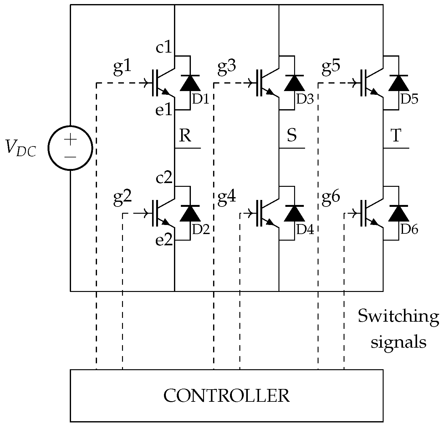
. In the case of a two-level three-phase inverter, the electronic circuit corresponds to that illustrated in
Figure 1, where there is a DC voltage source (
) and six switches in three parallel branches [
4]. In this case, the IGBT symbol has been selected to represent the switches, as they are common for the integration of renewable energy sources. The outputs are obtained from the connections with regard to the neutral point.
The variation of each output signal (between
and
) is achieved by alternatively closing and opening the switches of each branch. The phase shift of the three signals is achieved by adjusting the activation sequence of the switches. In order to generate the VSC switching or control signals, a wide diversity of methods has been studied and applied. Differences in their mode of operation have been developed to achieve one or more of the following objectives: wide linear modulation range, reduced switching losses, lower total harmonic distortion (THD), easy implementation and shorter computation time [
5,
6,
7].
Although inverters have been traditionally designed as analogue circuits, these converters are more often activated by microcontrollers nowadays [
8,
9]. Among the control methods applied by these microcontrollers, three different solutions can be highlighted: voltage input variation, pulse bandwidth variation, pulse width modulation (PWM), sine pulse width modulation (SPWM), or space vector modulation.
Since the use of microcontrollers is common, SVM has become one of the most important methods for three-phase converters. In this case, the space vector concept is used to calculate the duty cycle of the switches. Generally, SVM involves the sequence of the following phases: (i) sector identification, (ii) calculation of switching times, (iii) determination of the switching vector and (iv) selection of the optimal switching sequence for the inverter voltage vectors. In Ref. [
8], the authors describe an example of a modified approach to space vector modulation technique implemented on a low-cost PIC 18F4431 microcontroller. As stated by the authors, with this type of modulation it is digitally easy to implement the control of the switching devices.
Since the use of VSC is getting more widespread in applications such as renewable energy, high-voltage DC transmission (HVDC), the flexible AC transmission system (FACTS), and smart grids [
10,
11,
12], it is important to provide effective, simple and robust mechanisms to correctly perform the switching operation. The aim of this work is to propose a switching technique based on a finite-state machine (FSM), which stands out as a simple mechanism to generate the inverter control signals. FSM is a conceptual machine used to model the behaviour of objects. This behaviour is defined in different states. The transition through the states is caused by the occurrence of some events. Due to this conceptualisation, FSMs are more in accordance with the discrete performance of a programmable device such as a microcontroller, making these types of controls easier to implement and monitor. Finite-state machines have already been used for the characterisation of power electronics devices. The switching operation of power devices is characterised with this type of model for SiC MOSFET [
13] and for Si-SiC hybrid switches [
14]. In Ref. [
15], the authors propose a fault diagnosis method to detect multiple transistor open-circuit faults in a three-level T-type inverter with the support of a finite-state machine. As for the control, the suitability of FSM has also been validated for DC–DC converters [
16].
In Ref. [
17], we identified the states and transitions to describe a FSM for the switching control of a VSC. The main advantage provided by this control technique is its capability to be implemented in low-cost microprocessors. This promotes the reduction in costs in low-power renewable installations, such as those oriented for self-consumption. The simplification also helps to reduce the complexity of converter-monitoring. In addition to the simplification that this method provides, the proposal is able to maintain similar harmonic distortion than conventional methods such as PWM and SVM. This paper extends our previous work with four main topics: (i) the analysis of the filter to be placed at the output of the VSC, (ii) a comprehensive and theoretical analysis of the performance provided by the proposed switching technique under static and dynamic conditions, (iii) design of an optimised coding for the proposed control, which is valid for low-cost microcontrollers, and (iv) lab-test evaluations with a proof-of-concept.
The main contributions of this work are:
Proposing an effective and simple mechanism to proceed with VSC-switching based on SVM. The method is supported by a FSM, which enables the implementation of the method in current microcontrollers with computational and memory constraints.
Analysing the effects of the low-pass band filter in the proposed method.
Simulation-based study of the performance of the controller when there are changes on the grid’s main features or on the commands of the STATCOM.
Evaluating the proficiency of the proposed controller in comparison with PWM and conventional SVM. We observed similar harmonic distortion for the three switching techniques. The compliance with ANSI/IEEE-519 has also been verified.
Defining an optimal coding of the control so that it can be executed in a low-cost microcontroller, widely available in the market.
Evaluating the proposed control with a proof-of-concept implementation in our lab. There is good agreement between the simulated data and the measurements.
The rest of this paper is structured as follows.
Section 2 presents the details of SVM vector space modulation. Then,
Section 3 develops the proposed method, that is, SVM modulation based on a finite-state machine (SVM-FSM).
Section 4 addresses the design of the LC filter at the inverter output. In
Section 5, the performance of that proposed is evaluated with respect to PWM and SVM. The control implementation is described in
Section 6, while the experimental results are shown in
Section 7. Finally, in
Section 8, the conclusions are presented.
2. Space Vector Modulation: Fundamentals
For a VSC, there are two types of switching sequences. The first type consists in forcing the conduction to 120° electrical. This implies that the excitation signals for each switch last 120° and are conducted two at a time (
). The second option is based on the conduction to 180° electrical. In this case, three transistors are active at a time (
) [
18]. Imposing three switches to be active at the same time in this last approach allows higher power levels to be delivered to the load, so this is the most common option. However, short-circuits must be avoided [
19].
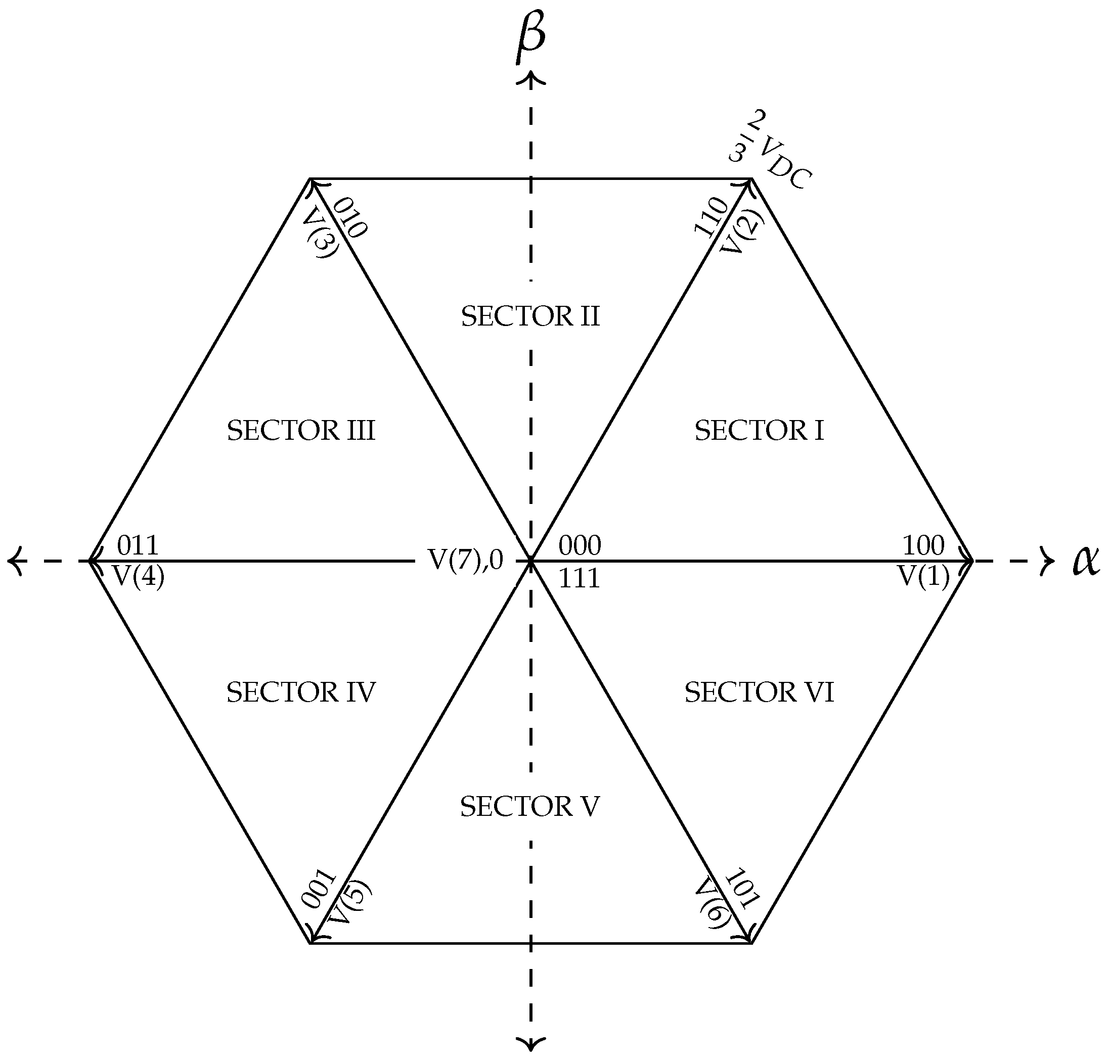
A different way to represent the alternating signals generated by the inverter is the consideration of a reference frame that rotates at the fundamental frequency of signals, obtaining a plane of two
axes, known as vector representation. To calculate the vectors, the Clarke transform Equation (
1) is used, obtaining the hexagon in
Figure 2, with seven voltage vectors and two null vectors. Each of these vectors corresponds to a combination of switches in the active state. For a conduction of
, the vectors are
apart, with a length of
. A more extensive description of the basic concepts of this transform can be found in Ref. [
20].
The voltages are listed in
Table 1. Each state/voltage (
) generated with the SVM is related to a group of three activation states (first column in
Table 1). These variables model
,
and
control signals in the order as they are mentioned. The variables
,
and
are complementary to the previous signals.
There is a variety of techniques used for the generation of switching trigger patterns. However, they can all be classified into sine modulation and the vector modulation technique. The latter consists of determining the linear combination of the virtual voltages (, and ) that conform the intended voltage () during the interval ).
The generation of the three-phase voltages is related to the variation of the reference voltage in a clock-wise way. Thus, every time during a complete period,
is in a specific position so that it must be modelled with a particular combination of the virtual voltages corresponding to the sector where it is placed. Thus, the modelling with the virtual voltages is time-dependent. The virtual voltages
and
depend on the sector on which the voltage is located. Each reference vector is active only during a fraction of the complete period
. Specifically,
contributes to the generation of
during
, whereas
is used during
, being
and
. In order to unify the concept to compare the PWM and SVM techniques with the proposed method, the switching frequency has been taken as
. To compute this combination, the following Equations (
2) and (
3) are used.
The goal of a SVM-based switching technique is to determine how long each vector must be maintained to get the virtual vector
. It is said that it is necessary to determine the
,
and
considering the vectors
and
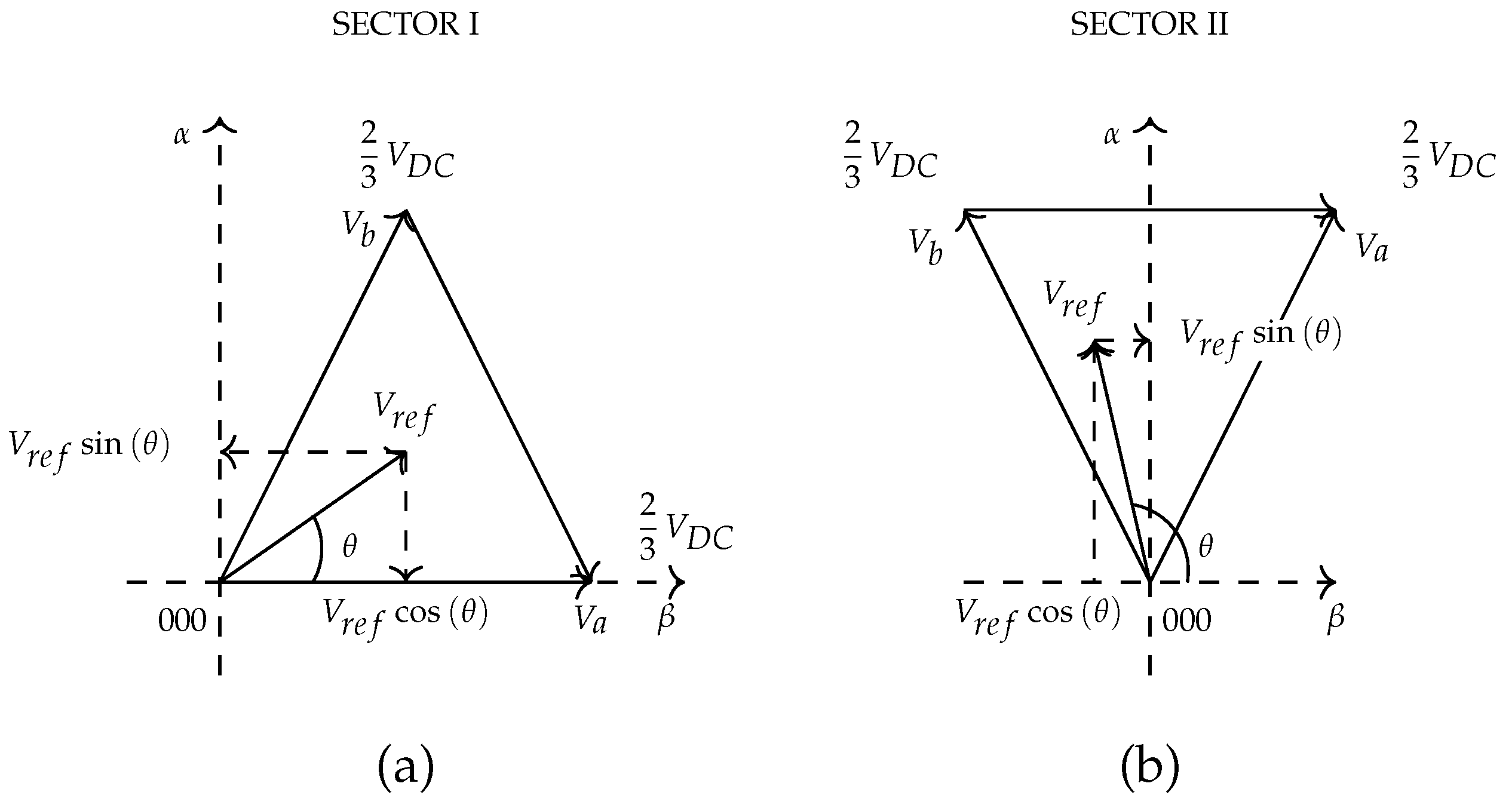
in each sector. As previously mentioned, these vectors depend on the specific sector in which the reference voltage is. For illustrative purposes,
Figure 3a shows the vectors
and
for Sectors I and II.
Supported by a trigonometry analysis, it is possible to derive the equations of the times associated with each sector, as shown in
Table 2. For a voltage value
in Sector
n with
, Equations (
4)–(6) are general expressions to calculate
,
y
times.
As the purpose of the inverter is to generate a three-phase periodic sine wave, then it is necessary to determine the electrical angle and sector by using a timer. Thus, the voltage
varies and the times
,
and
are accordingly computed. A dynamic determination of the sector must be accomplished. For a generic time instant
t, the electric angle
, where
is calculated. Then, the number of turns is determined, that is, how many times the value
is reached in
, and that number is subtracted from
to leave only the decimal part using the following formula:
. In this way, only the angle between
is obtained. Moreover, since sectors are separated by
(
), then it is determined how many fractions of
can be computed in the decimal part calculated above, using the Equation (
7).
3. SVM Supported by a Finite-State Machine (SVM-FSM)
Once the method for determining the electric angle and the sector at time
t is known, it is now possible to propose a finite-state machine-based space vector modulation methodology. The application of FSM to model the dynamics of the inverters is feasible due to the discrete nature of these power converters. Switching dynamics can be accurately modelled with a FSM, as mentioned in Ref. [
21], for the control of a dual bridge converter, or in Ref. [
22] for single-phase inverters. One of the advantages of using finite-state machines is that it makes their digital implementation more systematic and flexible. For example, it could be implemented in a programmable gate array, such as FPGAs, as in the case of Ref. [
23]. There are also published results for a photovoltaic power plant [
24], where the different operating states or operating modes of the PV plant are sub-models based on finite-state machines working cooperatively. The authors report that the approach seems suitable for simplifying the operating model for renewable energy sources and acceptable simulation runtimes.
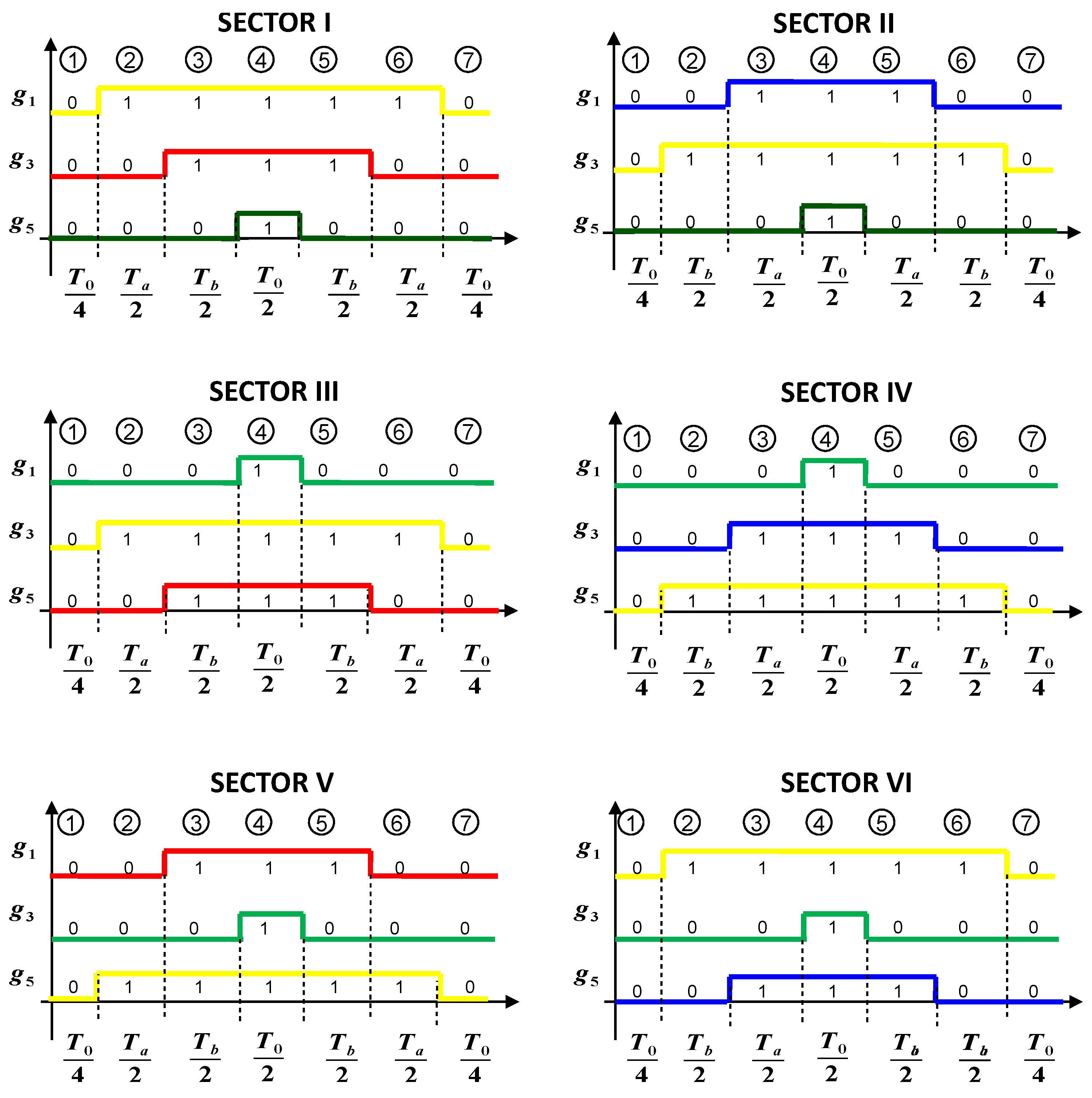
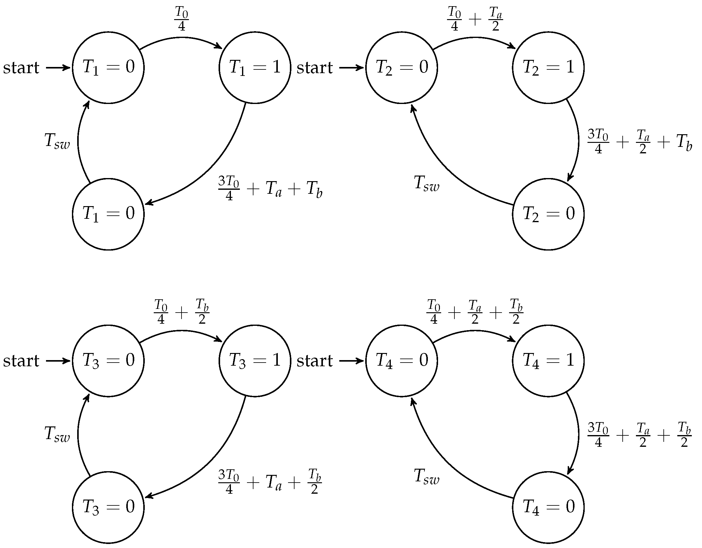
As described above, to generate an alternating waveform, switches are closed and opened as follows: a closed switch is fed with a logic 1 and an open switch is fed with a logic 0. In this way, a three-bit code can be constructed with the activation signals of the three upper-level switches (since the three lower-level switches are complementary). Therefore, when the upper level switch is active, the lower level switch on the same branch is open. In
Figure 4 the signals of the three upper level switches have been identified with
. It should be noted, as mentioned above, that in order to generate a virtual vector
,
must last for a time
,
must remain for a time
, and a time
for the null vector. The latter vector can be achieved with all the top-level switches
closed
or open
.
As it is recognised from digital techniques, it is important that the changes are one bit at a time. For example, if a reference vector within sector I has to be generated, combination
is used as vector
, combination
as vector
, and both
and
for null vector
. The sequence of these virtual vectors could be set out in multiple ways, but we will opt for that in which two successive virtual vectors used for the generation of
differ in only one bit. In
Figure 4, seven different combinations are generated for each sector. For the seven combinations, the intervals in which the signals
,
and
are constant have the same duration (
). Another detail that can be observed in all the time diagrams is that four pulses are interleaved. They are identified by colours in
Figure 4, and can be distinguished by their own duration: the first one is yellow and has a duration of
, the second one is red and it appears only in odd sectors, with a duration of
, the third is blue and it appears only in even sectors with a duration of
. The last one is green, with a duration of
. We use these patterns to model four finite-state machines associated to
,
,
and
.
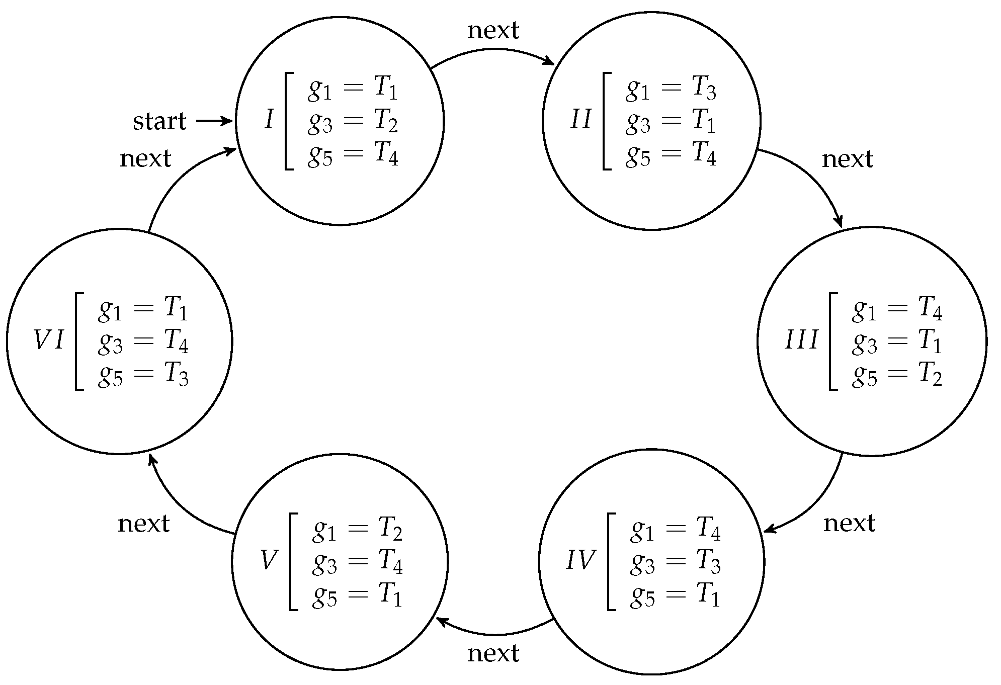
In addition, we also identify the fifth finite-state machine to assign to each gate the pattern corresponding to the sector in which
is placed.
Figure 5 shows the diagram of this FSM. We can observe the association of the gate and the time patterns and the sequence of the sectors in
Figure 6.
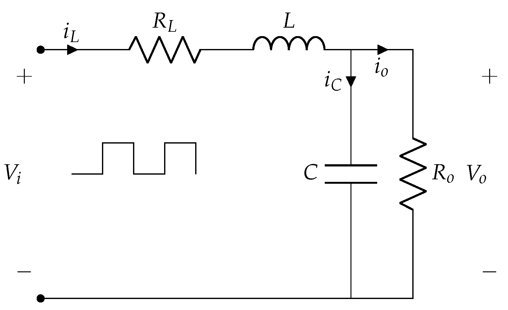
4. Design of the LC Filter
The output of the inverter is a digital signal. To derive a sine-wave signal, a low-pass filter is necessary. The low-pass filter is used to attenuate the low-order harmonics of the output voltage in order to minimise distortion of both linear and non-linear loads.
Figure 7 shows the most simple schematics for this type of filter, which is widely used in inverters connected to the grid [
25,
26]. It is composed of a capacitor
C and a coil with inductance
L and parasitic resistance
. The resistance
corresponds to the output load. There are different criteria to design this type of filter. We will proceed with a specific design based on the behaviour of the VSC and its modelling on a FSM.
With a circuital analysis, we can derive that:
where the cut-off angular frequency is defined as:
and the damping factor is:
In order to reduce the value of the inverter impedance, the capacitance must be increased and the inductance has to be minimised as a function of the filter cut-off frequency . This allows the cost, volume, and therefore, weight of the inverter to be reduced. However, the increase in capacitance leads to an increase in the inverter power with the rise of reactive power. Therefore, there is a trade-off between these three inverter parameters.
From the definition of inductance, the inductor voltage is determined as follows:
where
, and
is the maximum duty cycle for the switching control of the VSC. In
Figure 4, the maximum duty cycle is identified with the yellow signal, and its value corresponds to
.
To determine an approximate value for the duty cycle, the general expressions (
4)–(6) are substituted into the Equation (
11). The expression
is determined by simplifying Equations (
12) and (
13) and is shown below Equation (
14):
Taking
(sector I) and considering that the rest of the sectors are calculated in the same way, then:
In Equation (
13), we replace
, a value with which the overmodulation is avoided. As we are looking for the maximum duty cycle, then we choose
, which is where it takes the maximum value, resulting in Equation (
14).
This means that
. However, the standard requirements [
27] consider a limit of
, which corresponds with a
. Once the value of the duty cycle has been determined, an expression for the inductance
L can be obtained. The modulus of the complex voltage at the output of the inverter according to
Table 1 is
, which corresponds to the
of the filter, if the output
of the filter is limited to
and is considered to vary slowly with respect to the switching frequency. Then, the inductor voltage, which is given by
, leads to
. The value of the inductor
L can be obtained from Equation (
15).
The standard requirements [
27] also contemplate for the current variation
to be between 15–20% of the nominal current (
) of the inverter. The current variation can be determined from the inverter power (
and line nominal voltage (
), as shown in Equation (
16).
The SVM-FSM technique is going to be evaluated under the following conditions. The inverter feeds a load consuming a power of with a line nominal voltage V, where the fundamental frequency is Hz. The switching frequency is H, V, and the reference three-phase peak voltage value is V.
With these conditions, we apply the Equation (
16). The first step is to obtain the maximum current value for the inductor
A. Considering a current variation or inductor ripple of
, we have a value of
A. To calculate the inductance, these values are replaced into Equation (
15), with a result of
mH.
5. Analysis of the Proposed SVM-FSM Method
The evaluation of the proposed switching technique is performed in a simulation tool. Specifically, we have used Simulink/Matlab, which counts with the package Stateflow to model the finite-state machines [
28]. As described before, a control that generates a correct firing sequence in the switches and, thus, generates a three-phase waveform is essential. Therefore, a stage that generates the three waves with a
phase shift is needed. The total implemented circuit consists of three stages: the control stage based on finite-state machines (since the gates of the switches must be controlled under a periodic sequence), the sine wave generation stage constituted by the set of switches, and the filtering stage based on the LC filter. The state machines designed in Section
3 have been implemented in Matlab Stateflow. Another important aspect to be taken into account with respect to the state machine is the clock signal that controls the changes of the sequence generating both the angle and the sector. With these data, the times are computed, and it helps to check the conditions that lead to the transitions of a state.
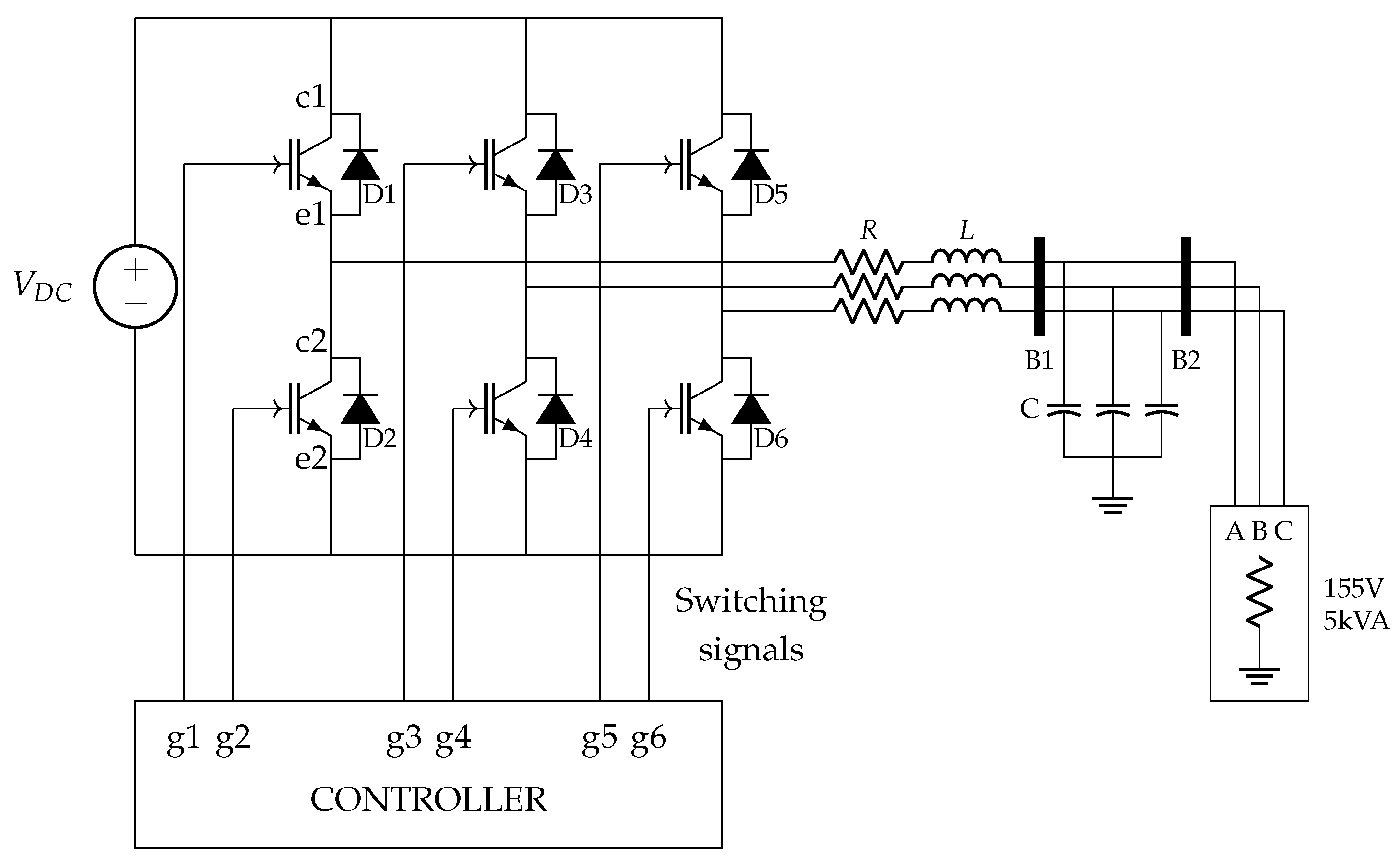
Pulse width modulation (PWM) and vector space modulation (SVM) generators have been implemented to qualitatively compare the designed SVM-FSM method and these two widely used generators. The inverter was implemented with the
filter feeding a 155 V, 5 kVA load, as can be seen in
Figure 8. The trigger pattern generator (controller) is located at the bottom, its outputs being the signals to activate/deactivate each switch.
Figure 9 corresponds to the submodel of the generator SVM-FSM. We have modelled the following blocks: (i) one block to determine the times according to Equations (
4)–(6) and (ii) the block to determine the sector, based on the Equation (
7). Then the state machine in
Figure 5 and
Figure 6 were also implemented in the block FSM.
The proposed control technique was evaluated with three types of tests. In the first one, the impact of the filter is analysed by varying the cut-off frequency. In the second one, the switching frequency is modified to see the effects on the performance of the finite-state machine. Finally, the load is varied to see the time response of the method. These three tests are described next.
The first test was performed to prove that the design of the low-pass band filter clearly impacts on the performance of these switching techniques, as the amount of harmonics and their amplitude depend on the features of this element. The first test consists of using the inductance
mH previously computed and applying the cut-off frequency equation. The three capacitance values for the three cut-off frequencies are shown in
Table 3. The effective voltage (
) and the total harmonic distortion of the load voltage have been measured for each generator for a sampling time of
s and a simulation time of
s. The results obtained for
and
are shown in
Figure 10 and
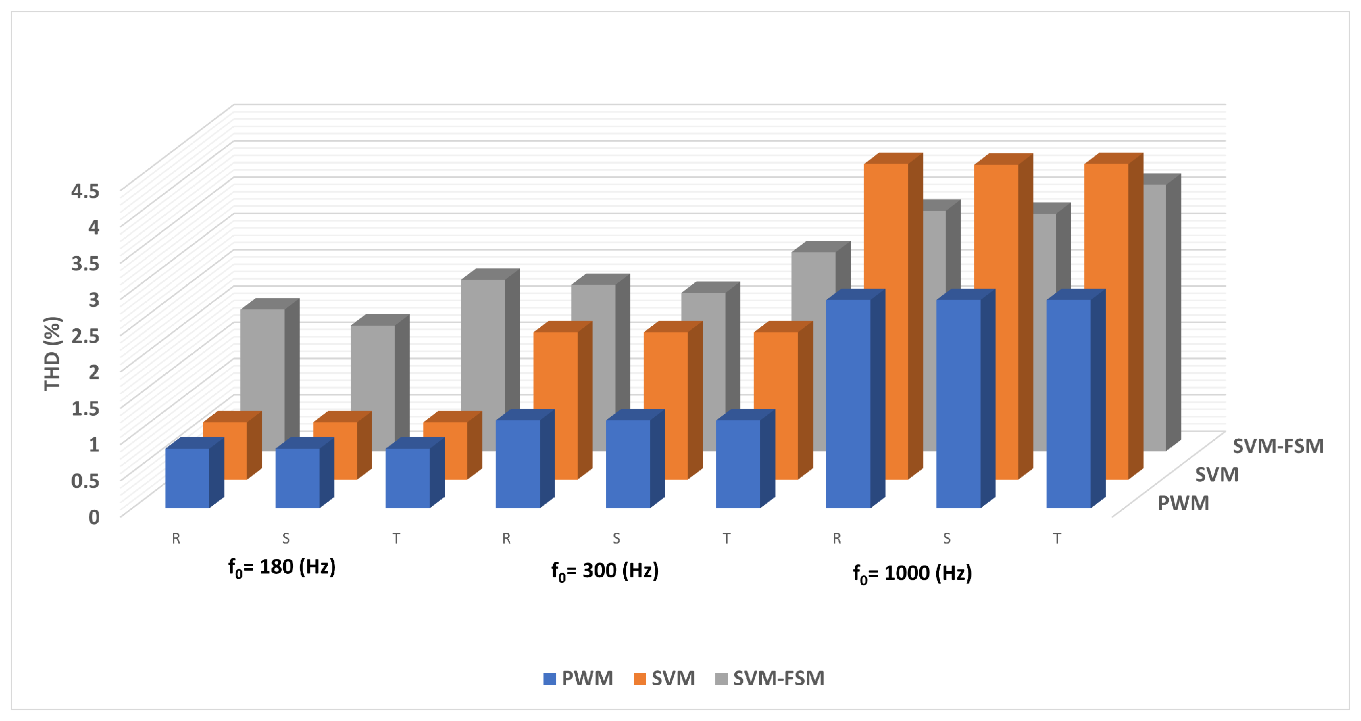
Figure 11, respectively, for each phase of the load output voltage (R, S, T). The distortion depends on the phase, as indicated in
Figure 11. The phases are affected by the non-lineal performance of the switching technique in a non-equivalent way. This phenomenon is observed for SVM and SVM-FSM.
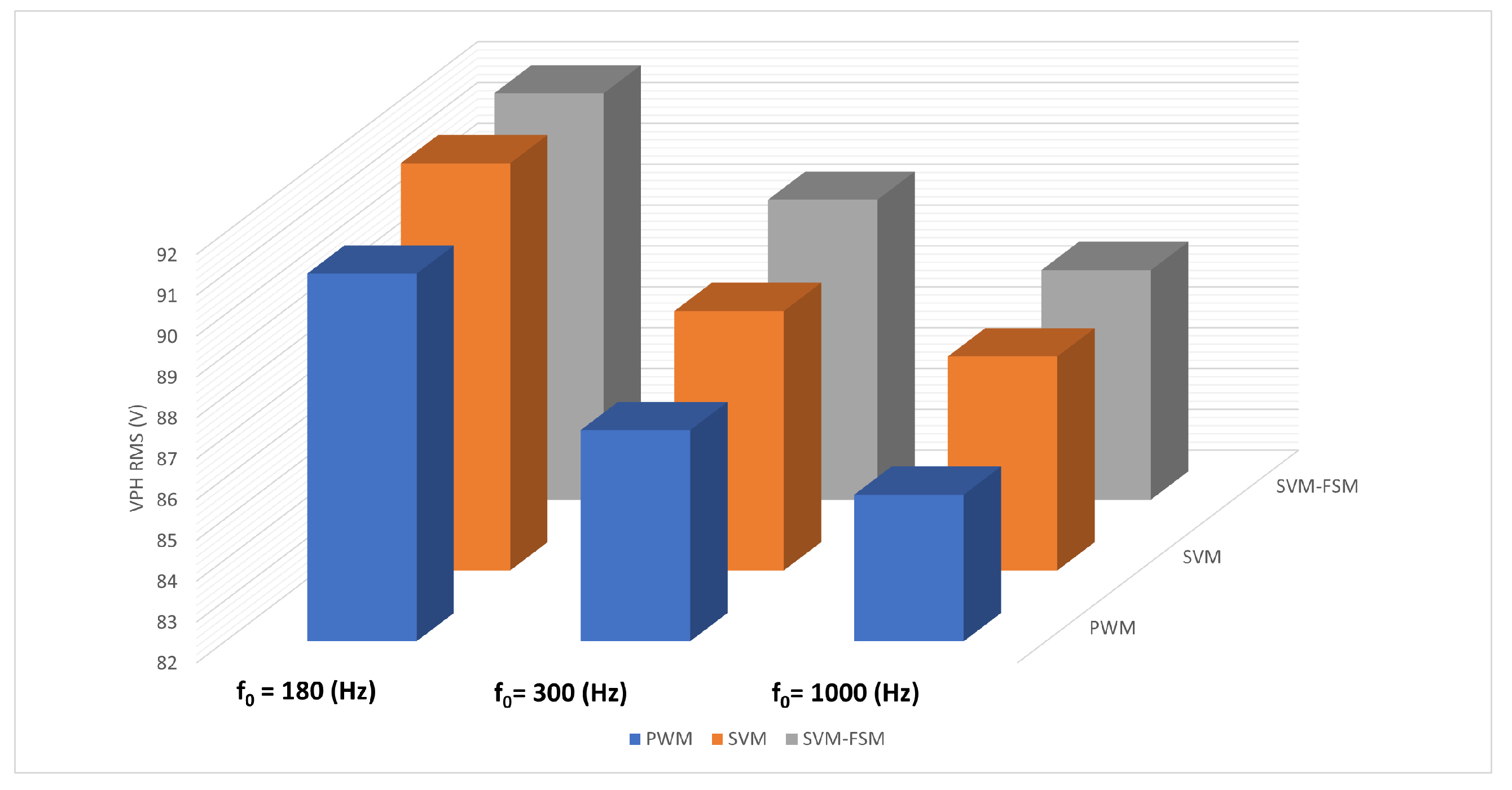
In
Figure 10 it can be observed that the effective voltage decreases as the cut-off frequency increases for all the configurations. The RMS voltage value (
) is similar in all three cases, with a maximum difference of 2 V localised between the PWM and SVM-FSM configuration for a cut-off frequency of 300 Hz.
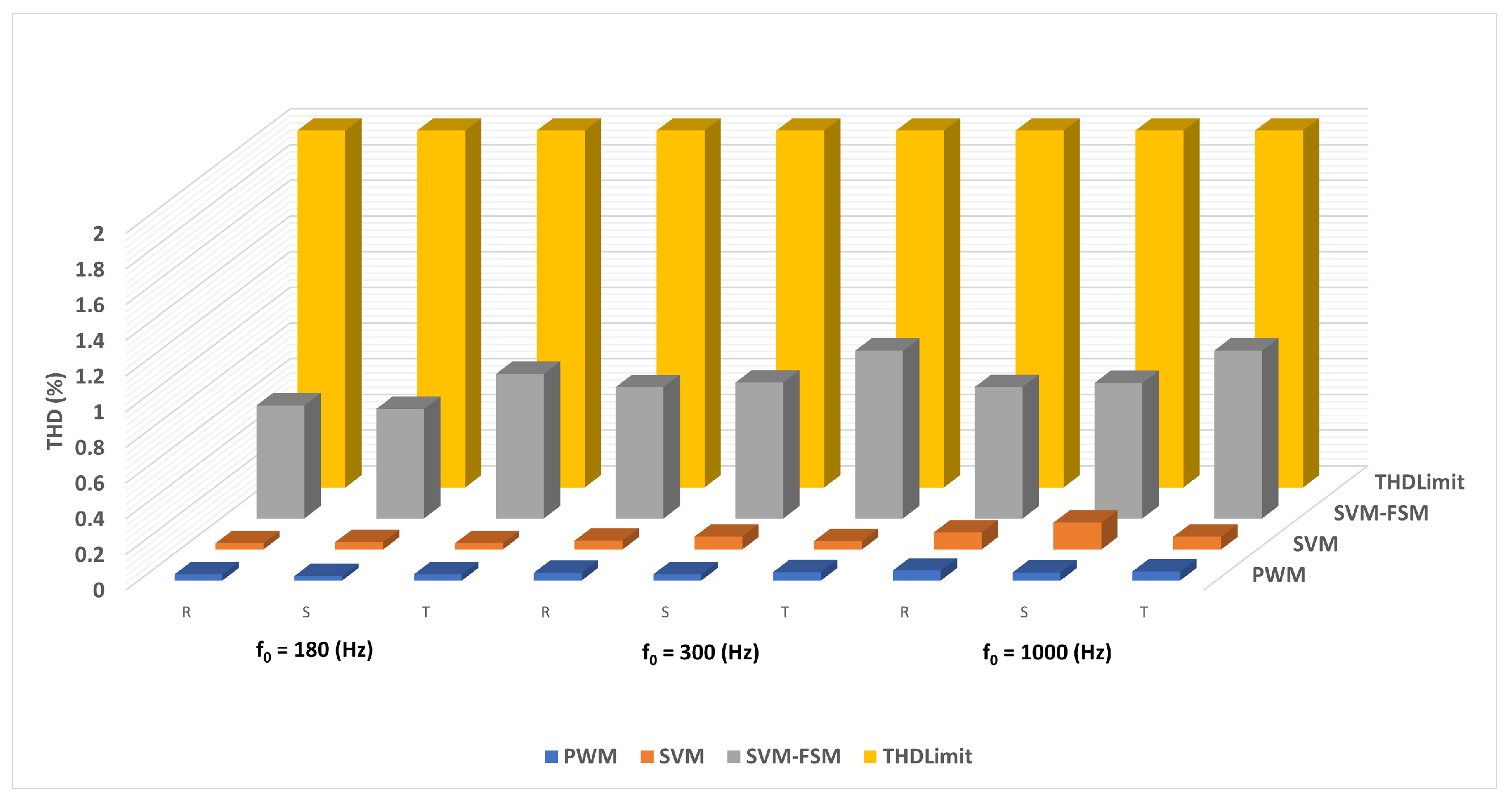
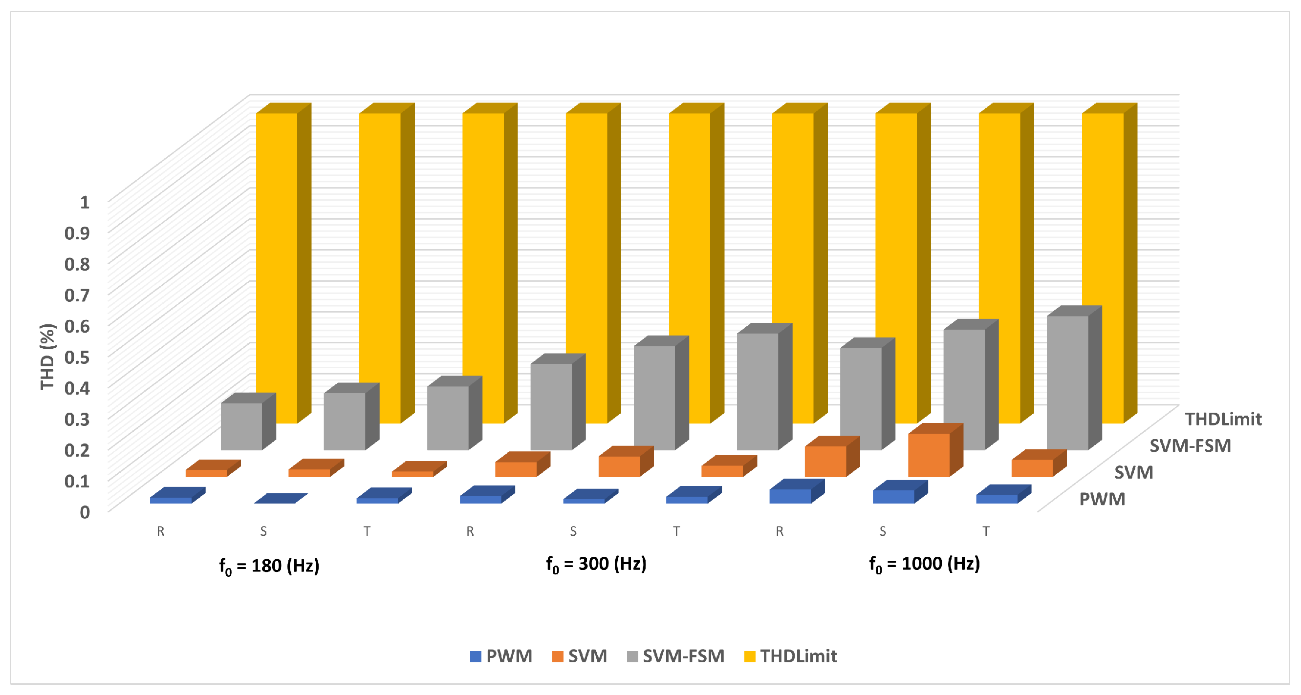
Figure 12 and
Figure 13 show an analysis of the THD levels obtained in two different Harmonic Order (HO) ranges, according to IEEE Std 519 (2014). It can be observed that the limit indicated by the regulations is not exceeded in any case, being 2% for the range
HO < 11 and 1% for the range
HO < 17.
The second test consisted of setting the filter cut-off frequency to
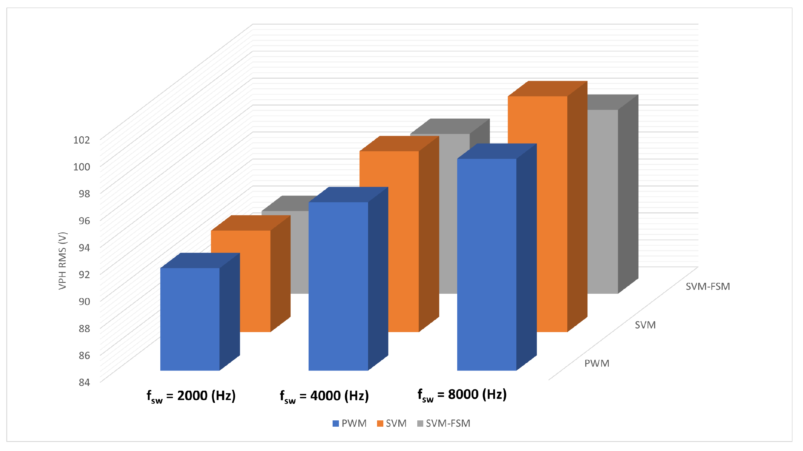
Hz, which, according to the previous results, shows the worst performance. We aim to evaluate the control technique and the effect of
in the worst condition to expand the usability of our proposal. Therefore, we increase the inductor current ripple to
and
A. Then, we compute the inductance and capacitance for three switching frequencies
Hz. The details about the configuration of the filter for these switching frequencies are summarized in
Table 4. In the same way, the (
) and
of the load voltage were measured for the three generators with
and a simulation time of
s. The results obtained are in
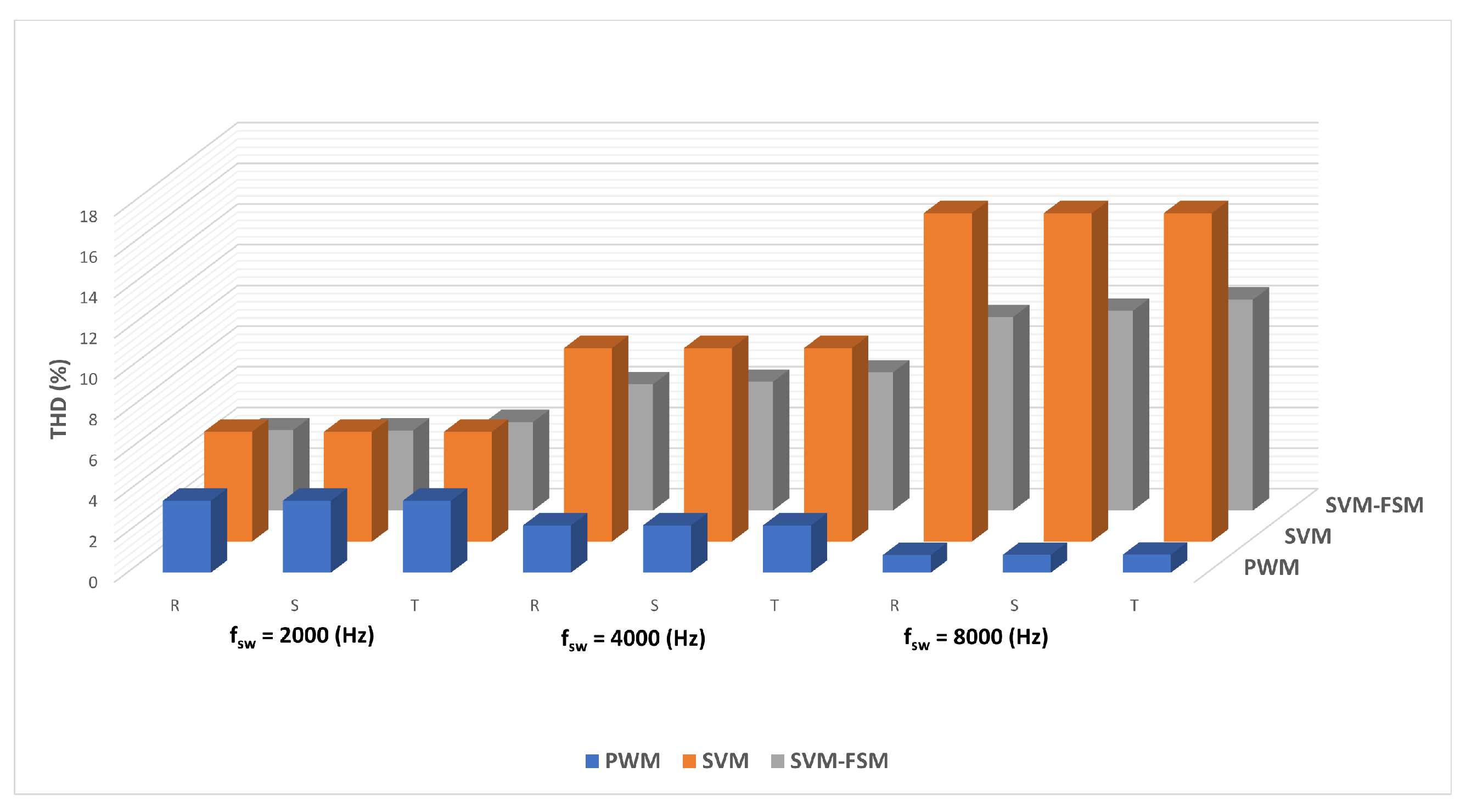
Figure 14 and
Figure 15.
Figure 14 shows a similar improvement for all three methods when we increase the switching frequency. For the proposed switching technique, there is an up to 9 V increase. In
Figure 15, the THD increases when
is higher. With this condition,
decreases and, therefore, the switching time of the switches between inverter branches is shorter. Consequently, the effects of the non-linearity of the inverter are more notable. Our method is robust since the lower the
, the better the performance is achieved. The best results are obtained at
Hz, that is, more switching time and therefore less power losses due to the switching effects [
29]. The complexity required for the microprocessor is also decreased as the operations can be executed in longer intervals.
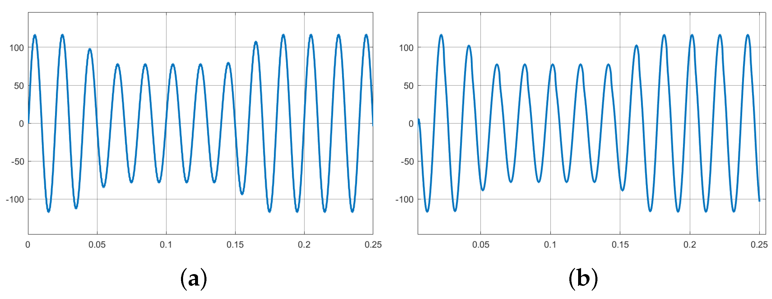
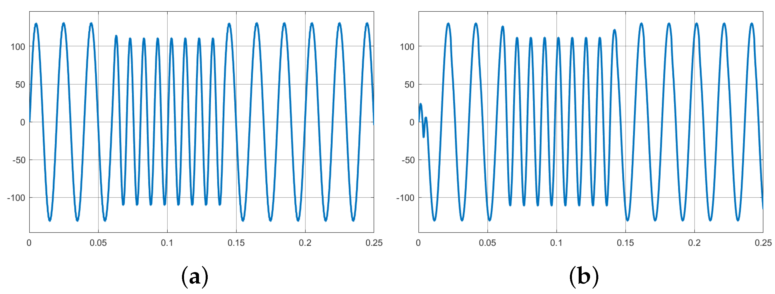
Finally, the technique has been evaluated when there are changes on the goal or grid conditions. The parameters established in these experiments are:
Hz,
and
Hz, where the filter results in
and
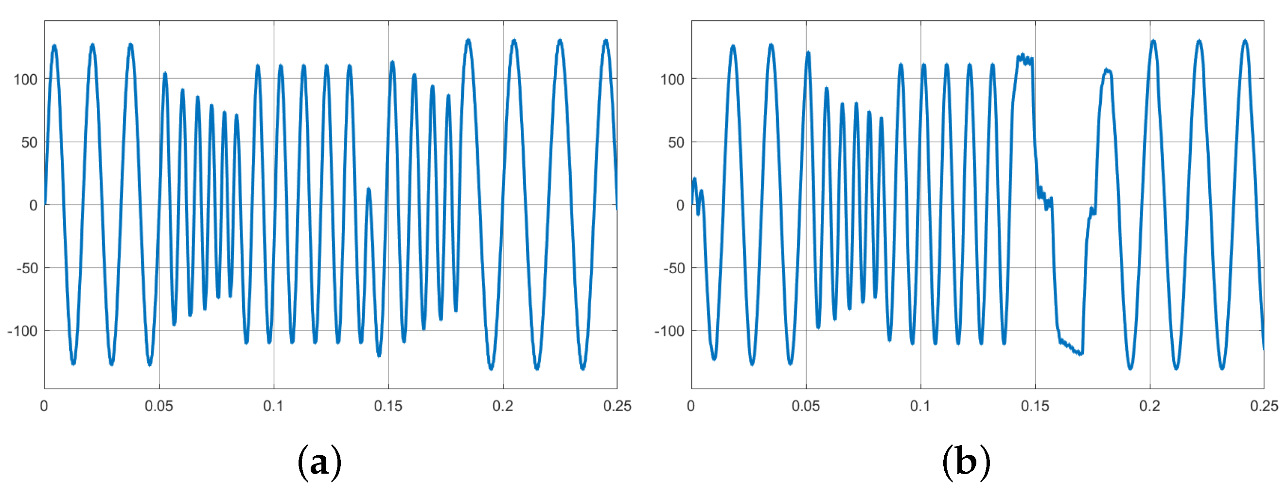
mH. Specifically, we have tested how the control performs when (i) the reference voltage is variable from 150 V to 100 V and back to 150 V; (ii) the fundamental frequency abruptly changes from 50 Hz to 100 Hz and back to 50 Hz; and (iii) the fundamental frequency varies gradually (with a ramp), from 50 Hz to 100 Hz and back to 50 Hz. The waveforms are depicted in
Figure 16,
Figure 17 and
Figure 18.
The simulation time was increased to
ms with the intention to observe the waveforms properly. As can be observed in
Figure 16,
Figure 17 and
Figure 18, SVM and SVM-FSM generators are compared. The results show that there is a response time that affects the synchronisation of the proposed method. It should be noted that as SVM-FSM is a discrete generator, jumps in the signals are more noticeable than in the case of SVM.
The developmental steps, design, and performance evaluation of the proposed method showed that it is easy to implement, which is the greatest strength of the proposal. However, it presents a dependence on the switching frequency, since the method is based on event dynamics.
6. Control Implementation
One of the main goals of the control technique is to achieve an efficient and easy to implement method to switch the power devices. To do so, we carefully programmed ESP8266, a low-cost microprocessor available at most popular electronics dealers. The microcontroller has a L106 32 bit RISC microprocessor running at 160 MHz, with a 32 kB instruction RAM and 80 kB RAM of data. In addition, it has 17 general-purpose input/output pins and wifi, SPI, I2C and UART communication protocols. Considering these restrictions, the coding of the instructions must be well designed to allow the switching frequency intended in the application under study.
From straight-forward coding of the FSM, we identified the more time-consuming instructions in order to optimise their execution with alternative programming. In our coding, we needed to generate a 50 Hz signal with a switching frequency of 2 kHz. This implied that the changes on the must be performed every 500 s. Thus, the following instructions needed to be optimised:
Computation of the times and . As they require trigonometric operations, they are more time-consuming. In fact, after measurement, we found that they require almost 300 s in the microcontroller considered for the application.
Unnecessary loops which add extra time to the execution of the main programme. These loops are associated to the modelling of the time patterns , , and individually.
Redundant computations that can be simplified. For instance, in the traditional coding of the SVM, the time is computed in each iteration, and from this, the sector in which is placed must be determined so that the correct operations are executed. This operation can be simplified as the position of in two consecutive iterations is in the same sector, or it has moved to the next sector. Most simple operations can be executed to check if the reference voltage has changed to the next sector.
To overcome the aforementioned limitations, we have proceeded with a code optimisation. This process has been achieved with the following steps:
Memory preallocation of the times and with a precision of 1°.
Memory preallocation of the sector S with a precision of 1°.
Joint implementation of the four finite-state machines , , and in order to reduce the computational cost.
Once the key factors have been identified, we proceeded to code PWM and SVM so that the performance of the proposed switching method can be evaluated in an experimental setup. Results showed that the memory usage for these control techniques with the same microcontroller was 17,896 bytes, 18,296 bytes, and 19,688 bytes for PWM, SVM, and SVM-FSM, respectively. With this parameter, it can be observed that PWM is the most simple implementation. SVM requires some additional computations to determine the sector, which increases the memory usage. Finally, SVM-FSM makes use of a pre-allocated table, which results in an augmented memory usage.
Algorithms 1 and 2 shows the two pseudo-codes considered in this project. Algorithm 1 stands out for the direct implementation of the method with a simple sequence of phases. Algorithm 2 is the optimised version of the code with a memory preallocation of the times and sector and a joint implementation of the FSM related to the time patterns. The optimisation process was released in order to reduce computational costs and times as computations with a relevant time consumption were eliminated and replaced with a predefined array of values depending of the current angle. With this optimisation, we aimed to reduce the execution time of a loop to 37.4
s.
| Algorithm 1:Simple implementation |
- 1.
while (1) - 2.
Compute time - 3.
Compute angle - 4.
Compute Sector - 5.
Compute Ta - 6.
Compute Tb - 7.
Compute T0 - 8.
States Machine T1 - 9.
States Machine T2 - 10.
States Machine T3 - 11.
States Machine T4 - 12.
States Machine Switching - 13.
end while
|
| Algorithm 2:Optimised |
- 1.
Define Ta, Tb, T0 and S - 2.
while (1) - 3.
Compute time - 4.
Compute angle - 5.
Prestored value of Ta, Tb, T0 and S - 6.
States Machine T1, T2, T3, T4 - 7.
States Machine Switching - 8.
end while
|
7. Experimental Evaluation
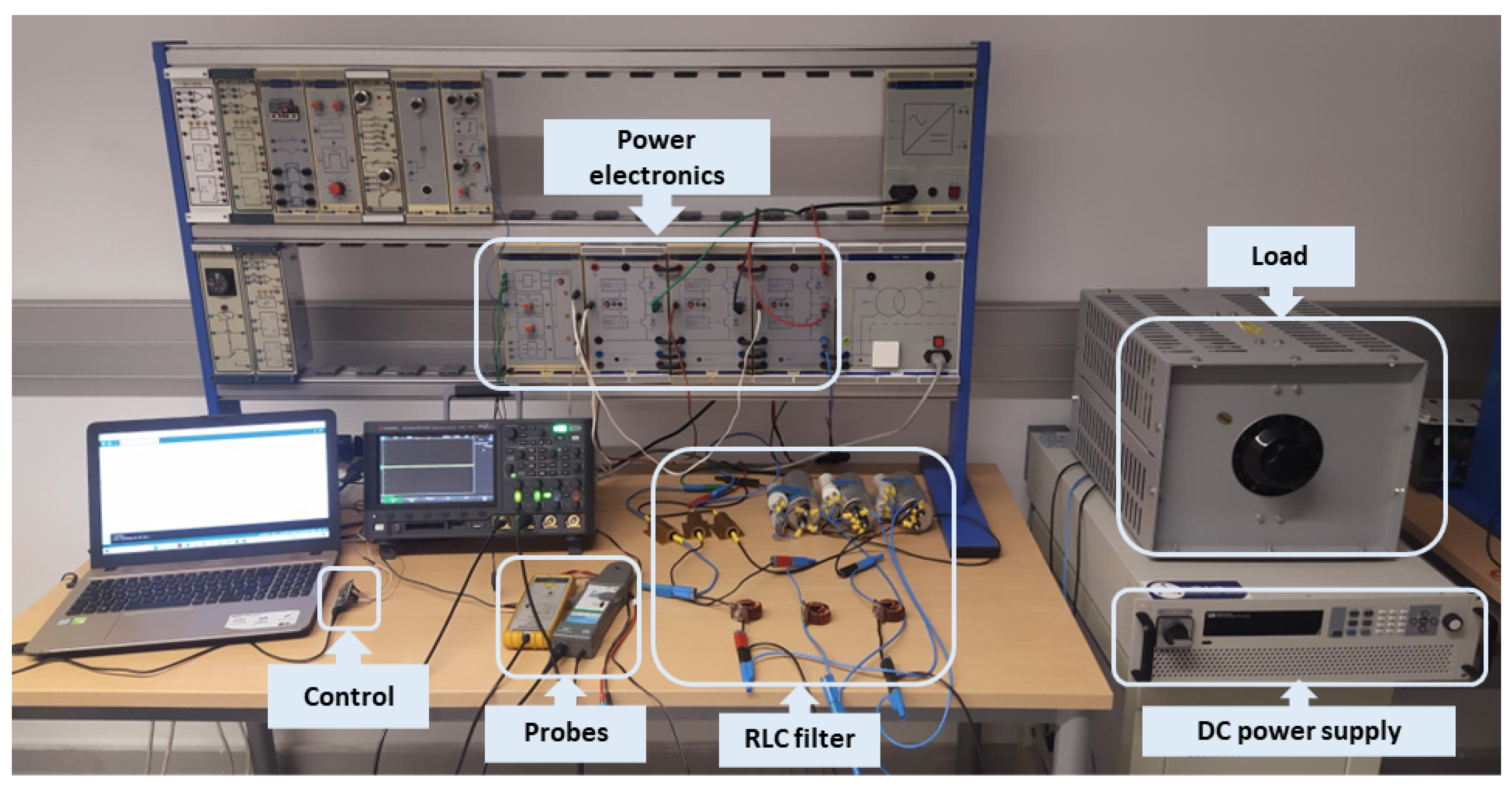
In order to evaluate the effectiveness of the proposed switching technique, we implemented it and two other well-known methods in a real laboratory setup. We illustrate the lab setup in
Figure 19. The setup consists of a set of IGBT modules which can be used for a three-phase inverter. These modules have all the necessary security elements, such as short-circuit and over-voltage protections. In addition, these modules also have the necessary drivers to activate the IGBTs.
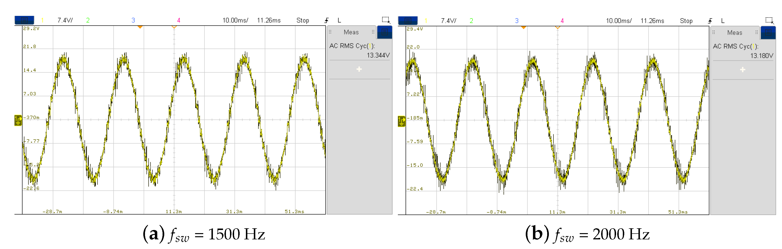
Simulated and experimental results have been compared. The experiments were implemented for the three different control systems: PWM, SVM and SVM-FSM. Two different switching frequencies have been considered: Hz and Hz. Due to the nature of the FSM-SVM algorithm, there are 80 changes from 0 to 1 and 1 to 0 in the IGBTs per AC cycle (for 2000 kHz of carrier signal). In a period of 0.02 s (50 Hz), the IGBTs switch 40 times. The same performance was perceived with PWM and SVM implementations where the carrier was also implemented at 2000 Hz. For an implementation of 1500 Hz, the switching cycles change from 40 to 30, due to its larger period.
VSCs are usually operated with higher input voltages, but due to the laboratory constraints, the maximum input voltage we could test was 50 V.
Table 5 and
Table 6 show a comparison between the simulated and experimental values for the load phase voltage. The experimental results show the same trend as the simulation results. Slight variations can be observed in the experimental results due to the effect of the losses produced in the power converters that have not been considered in the simulation. Comparing the different methods, it can be seen that the RMS voltage values achieved with SVM-FSM are, in most cases, moderately higher than those of the other methods for the same input conditions. It should be noted that, when the switching frequency was varied from 2000 Hz to 1500 Hz, no significant changes in the RMS voltage value were observed.
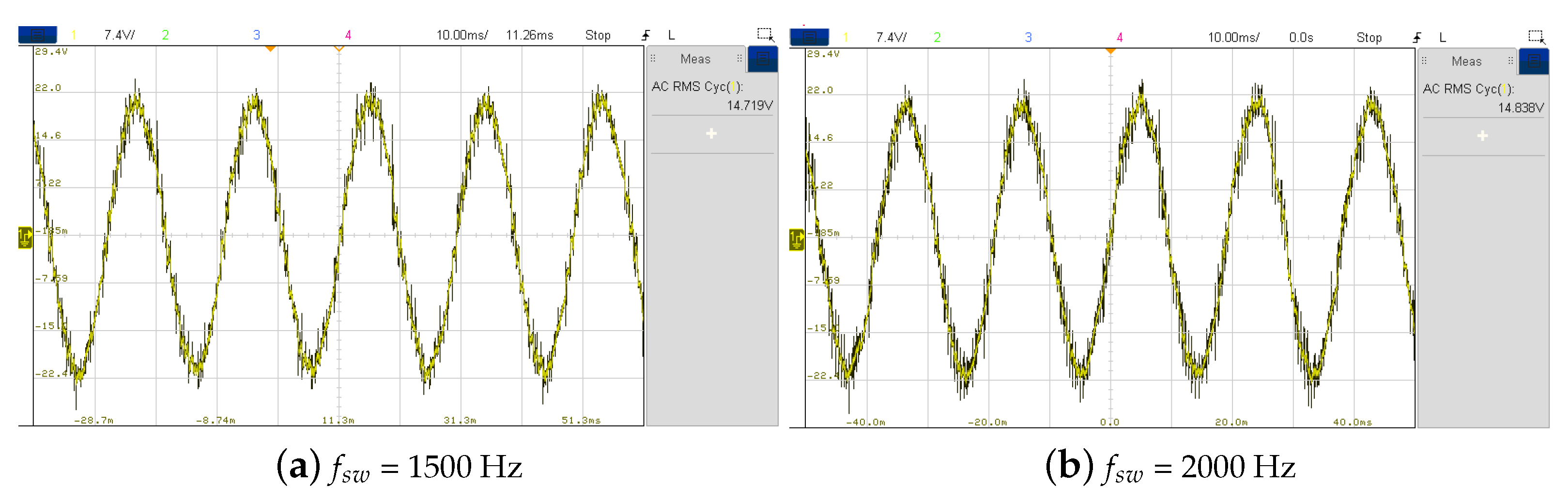
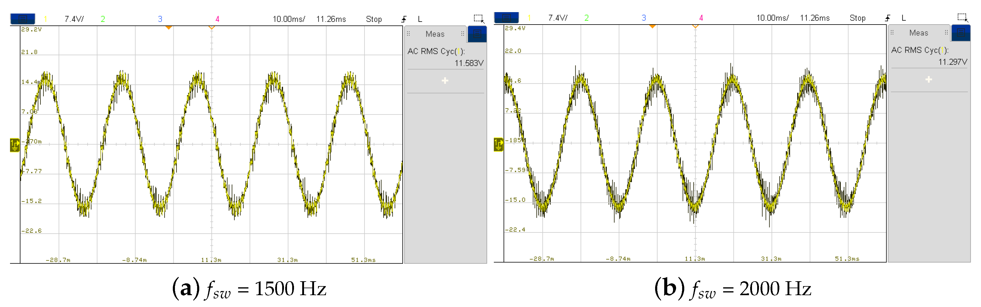
Figure 20,
Figure 21 and
Figure 22 show the filtered phase R for the SV-FSM, PWM and SVM techniques. The RLC filter was implemented as described in the previous section. The cutoff frequency was established in 180 Hz with
,
mH and
. The sinusoidal wave with some added harmonics could be observed, which was a common feature in the three methods tested.
In addition to the comparison in terms of RMS voltage, an analysis of the THD was performed to each
to ensure that the proposed method is compliant with the standard IEEE Std 519 for each technique, both in the simulated and experimental cases. In
Table 7 and
Table 8, the obtained results can be observed. As stated, the divergence between simulated and experimental results is not very significant. These differences may be due to the non-ideality of the filter for the experimental case, which can lead to slight variations in the characterisation of the components. Passive components can also have parasitic parameters that have not been considered in the simulation. Additionally, it has been observed that the differences found between the cases
Hz and
Hz are not remarkable, but also indicates a strong correlation between non-linearities and the frequency of the case of study, resulting in an inferior THD when the frequency is lower. The non-linear performance is not equivalent for the three phases, due to the fact that the processing times in the microcontroller do not affect each phase in a uniform way (the angle at which there are some deformations on the sinusoidal wave is different for each phase). This could explain the differences on the THD for each phase, as it has already been identified in Refs. [
30,
31]. Moreover, these effects are strongly dependent on the switching frequency and on non-perfectly balanced loads. A deep analysis should be performed to avoid this effect, which was present in the three switching techniques tested. The work in Ref. [
32] argues that the modulation index should be carefully set to avoid some of these effects.
Table 9 shows the efficiency results obtained in the laboratory implementations. As can be observed, SV-FSM has the highest efficiency compared with SVM and PWM. The efficiency levels are relatively low due the fact that our experimental setup was implemented with low power transfer. Under these conditions, the losses of the switches and other non-ideal components may be comparable to the levels of the power transfer, which derives from low efficiencies.

 ,
, 


