1. Introduction
Manufacturers are shifting to cheaper and faster production in response to the rising demand for electronics. To speed up design and reduce costs, unreliable, low-cost centers are responsible for building these components, leaving ICs vulnerable to enemies. One critical challenge in this field is the insertion of hardware Trojans (HTS) in integrated circuits. HTs refer to malicious modifications to circuits to leak secret information or change the performance or functionality of the design. These modifications are added maliciously to the original design by the attacker for specific purposes. A hardware Trojan consists of two parts, including a trigger and payload. It is activated by the trigger output signal propagation toward the payload; the attacker controls this signal. Trojan insertion is performed in several ways, including changing one or more bits of the bitstream configuration for one or more look-up tables (LUTs), changing routing elements and flip flop (FF) contents, or inserting tiny pieces into the original design.
Enemies try to hide Trojans so that traditional manufacturing tests would not be capable of detecting them. As a result, Trojan testing and detection mechanisms are costly and have a low success rate. The timely application of preventive techniques can help protect ICs against attacks by hardware Trojans. One way to prevent hardware Trojan insertion is hardware obfuscation. The circuit’s functionality becomes obscure for the attacker using this method, and reverse engineering becomes difficult. One method of hardware obfuscation is the logic locking of ICs. By inserting additional logic into the circuit, its functionality is in two states, normal and obfuscated. The correct key is activated in normal mode [
1,
2] if the correct key is available.
Enemies try to insert HTs into the original circuit design so the circuit can be exploited away from the designer’s view and operate properly in its natural state. They change its functionality when they want to disrupt or abuse the circuit. As a result, they frequently use untested signals in normal test patterns. HTs are inserted into trivial or unused hardware spaces. In a nutshell, they use small, unused spaces and low testability signals. For this reason, conventional test patterns cannot detect hardware Trojans and require new and expensive test patterns.
Timely use of preventive techniques can protect ICs against hardware Trojan attacks at a lower cost. One way to prevent hardware Trojan insertion is hardware obfuscation. Obfuscation techniques transform one design into another form that is still similar to the original executable design, while the new design is more resistant to enemies. Additional logic is inserted into the hardware to hide the original design’s structural and operation characteristics, preventing hardware Trojan insertion by untrusted factories. Key gates are inserted gates that use a key-based design for obfuscation. Obfuscated designs are those in which the design is obfuscated, and the user enters incorrect keys, resulting in incorrect output.
In recent years, various methods for hardware obfuscation have been proposed, one of them being logic locking. In logic locking, by adding several key gates to the main Netlist of the circuit, the function of the circuit is locked to the attacker. Various logic locking methods have been presented, and new attacks have been designed. Different logic locking techniques are defined as random, fault analysis-based, key interference-based, and one-way function-based logic locking [
3,
4].
In the fault-based logic locking method, the key gates are placed in the circuit locations obtained in the fault analysis. In interference logic locking, key gates are added to the circuit in a dependent manner. In one-way function-based logic locking, the key used in the key gates is generated using cryptographic functions or algorithm [
3,
4,
5,
6,
7].
Fault-based logic locking is less used because it can be extracted by fault analysis tests and has little resistance to attacks. Locking logic randomly, while having low complexity, because it adds key gates regardless of the circuit design, may be placed in the wrong places of the circuit. The interference logic locking method is more secure than the previous two methods because the keys are interdependent, and the attack successfully finds all the keys. Generating keys is one of the security challenges of logic locking methods. Key generation using cryptographic functions and algorithms can increase the level of security and complexity of attacks [
3,
4].
For criteria to calculate security, different logic locking methods are proposed. Criteria such as output corruptibility, clique size, number of distinguishing input patterns (# of DIPs), percentage of key bits recovered, and execution time can be expressed to evaluate the security level of logic locking methods. The amount of output corruption is the Hamming distance between the correct output and the output obtained when an incorrect key is provided. The number of key gates that interfere with each other is called the clique size. Distinctive input patterns are special input patterns that contribute to the success of key-pruning attacks such as SAT. The execution time of an attack can also be used to demonstrate the resilience of the logic locking technique against attack. Sometimes, certain attacks may achieve correct output by only finding a subset of key bits. The success rate of these attacks is determined by the percentage of key bits that are correctly recovered [
7].
Today, the security of integrated circuits seems necessary to prevent the insertion of hardware Trojans. Papers [
8,
9,
10,
11] have presented methods to prevent the insertion of hardware Trojans. They are examined in detail in
Section 3.
In references [
8,
9,
10,
11] hardware redundancy and delay are greater than usual. In this paper, our effort is to provide a method that can reduce the delay and hardware overhead while maintaining the positive features of the previous methods.
The critical challenge of digital technologies is outsourcing production and manufacturing to foreign centers due to the need for quick and low-cost construction. Therefore, the security of the hardware is jeopardized. On the other hand, the integrated circuits have become small and fast; consuming space and high delay are not acceptable to secure them. Researchers should propose security solutions for hardware by reducing the overhead of consumed space and delay.
This research is one with practical goals, facilitating the development of practical knowledge on the hardware security of integrated circuits to prevent the insertion of hardware Trojans. This research is quantitative research in which the simulation tool is used. We used the descriptive method to validate simulation software on the Netlist of standard benchmark circuits. The things that make this research different from previous research in providing hardware security in the design stage for integrated circuit factories are as follows:
We considered the need for more hardware space for new integrated circuits to add the number of key gates.
We paid attention to the speed of today’s integrated circuits and considered the amount of imposed delay.
We reviewed new attacks and considered resistance against them.
The remainder of the paper is structured as follows.
Section 2 reviews relevant work in recent years. In
Section 3, the primary purpose of the paper is stated, and the steps of the Secure Interference Logic Locking (SILL) method are described.
Section 4 elaborates on the steps of implementing the proposed method.
Section 5 compares our proposed method with similar methods presented in [
10,
11]. Finally,
Section 6 concludes the paper.
2. Background
HTs are malicious circuits intentionally inserted into the system to change the performance and functionality of the design. Sometimes, these changes are applied to the circuit to disclose essential and confidential information (sometimes, this malicious circuit is designed for information leakage without modifying the system specification). They are sometimes used to change the functionality of the original design. They are also sometimes utilized to gain control of the system, and the attacker’s purpose is sometimes to fail the circuit. Recently, various solutions have been proposed to detect and prevent hardware Trojan insertion [
10,
11,
12]
It is challenging to test and detect malware due to its specific nature (malicious and intentional changes). On the other hand, the attacker must have enough information about the original design to make the most of it. Prevention techniques should consider these two points. So, the original design must be hidden from the attacker.
It has a small unused space between normal operating cells. Enemies may use these small slots to insert HTs. Therefore, designers often try to fill unused spaces with non-operating filter cells and drastically increase the circuit’s compression. On the other hand, malicious factors can quickly and easily identify the filled circuitry spaces and fill them with a malicious circuit. Therefore, the filled space must be hidden to prevent HTs from being inserted with hardware Trojans.
Another solution is to obfuscate the original design (circuit and design functionality) from an attacker’s point of view. Reverse engineering becomes complicated for the attacker as the obfuscation becomes complex. In this technique, the design is obscure; therefore, the attacker cannot analyze the circuit to manipulate the design. By obfuscating the ICs, the circuit will function properly if the correct key is inserted. Moreover, eavesdropping may not be effective because the validity of the outputs depends on the correct key insertion, which is hidden from the attacker. Therefore, the correct functionality of the design is hidden from the attacker, who thus cannot disturb it. Various obfuscation methods have been proposed, including logic locking.
2.1. Hardware Obfuscation Techniques
Obfuscation is a powerful tool to hide circuit design from enemies. Hardware encryption methods and obfuscation techniques hide communications between chips while keeping input/output signals secret. Furthermore, the functionality of the original design is hidden from the attacker by using logic locking methods. Obfuscation techniques are divided into the following three types [
3,
13,
14,
15]:
It is a key gate logic-based obfuscation technique developed by the Chakraborty Research Group in 2009, which many researchers later improved. The idea behind this technique is to apply additional logic to the original design. Additional logic key gates are XOR/XNOR and MUX. Operational obfuscation makes reverse engineering extremely challenging. Therefore, untrusted factories will need help to fully understand the design under construction, and it will be challenging to insert hidden HTs into the obfuscated design [
1].
This method prevents enemies from gaining access to the input/output signals and altering or controlling them to activate the Trojan. Signals will be hashed, and circuit launch will only be possible if the design is obfuscated by implementing the wrong keys. They must use a coding method for their input to synchronize the operation of different circuit parts. Waxman et al. recommend using a uniform encryption method to make encrypted input data for the system as simple as possible [
16].
Study [
2], for example, presents the EOP solution for reducing these threats. EOP uses the flow encryption method to encrypt internal chip communications. Encryption and decryption are possible thanks to dedicated clock modules in this case. These modules ensure that the flow encryption is correctly synchronized while preventing manipulation. In addition, EOP employs a printed circuit board (PCB) level obfuscation method to protect the equipment from reverse engineering and introducing hardware Trojans (
Figure 1).
Figure 1 depicts blocks of various colors. The blue blocks are encryption-capable circuit components, while the yellow blocks are obfuscated circuit components that can form secret encrypted communications with the blue blocks. The chips must support encryption (blue block), and the yellow blocks employ all obfuscation techniques to ensure hardware security [
2]. Because the circuit parts in the green blocks lack encryption capabilities, all communications must be normal. The encrypted communications are indicated by the dotted arrows, while the continuous arrows indicate normal communications. The circuit section with obfuscation and encrypted communications is, of course, the most secure.
2.2. Logic Locking Techniques
Combined logic locking is a method of hardware obfuscation. This method adds a group of key gates to the main design. The operation circuit will produce the correct output when the correct key is pressed on the locked inputs. By controlling the key registers, the locking mechanism adds XOR and MUX gates to specific circuit paths (
Figure 2). Study [
4] presents an Anti-SAT attack approach. It complicates SAT attacks by increasing their key size, making them computationally infeasible.
This thesis must include an anti-manipulation chip protector (the AntiSAT) to prevent internal signal searches in the memory of the key chip.
Various studies have presented various methods for selecting appropriate key gate-adding signals. Randomly adding key gates to the circuit (random logic locking), in locations in the test patterns with high error probability (fault analysis-based logic locking), or adding key gates to create interferences in the circuit (key interference-based logic locking) are some of these methods [
3].
These methods are thoroughly described and compared in studies [
5,
17,
18]. In addition, we summarize them in the following section.
The XOR/XNOR keys are added to random locations to lock a design using the random logic locking method. A random logic locking sample with two K1 and K2 key gates is shown in
Figure 3a. The key gates are distributed evenly throughout using random logic locking. The random nature of this method is due to its lack of attention to the main circuit design while adding the key gates, making it vulnerable to attacks [
3].
Logic locking based on fault analysis aims to eliminate chip black boxes. For specific patterns, random logic locking may produce correct outputs with incorrect keys, but fault analysis-based logic locking guarantees a maximum output corruption rate when incorrect keys are used. When using the wrong keys, output corruption is the difference between correct and incorrect outputs.
Fault analysis-based logic locking places key gates in high-fault-tolerance locations. The effects of incorrect keys will be the same as those of stuck-at faults in the key gate outputs. Therefore, fault analysis/simulation software can pinpoint the most efficient location in any circuit. The fault analysis-based logic locking method is used to lock in
Figure 3b. Because the key gates are often inserted back-to-back, the logic locking security is weakened because multiple correct key values are created [
3,
5,
19].
Strong logic locking, also known as key interference-based logic locking, reduces vulnerability by maximizing key gate interferences. As the interference between key gates grows, the attacker is forced to examine several key combinations [
5].
For example, consider
Figure 3c. The K1 and K2 key gates, inserted using the key interference-based logic locking method, are included in this. K1 and K2 create interference in the path of their main outputs, as can be seen. As a result, the attacker cannot determine the K1 or K2 sensitivity to an initial output. All keys must be available to restore normal circuit operation, and more than a single key will be required.
The logic locking block considers two encryption blocks with different keys for function-based input. They will need more than one key for each input to obtain to the correct circuit output. By accepting more overhead, this method improves security.
The g1 and g2 functions generate the K1 and K2 keys, respectively, while their AND function generates the final key, as shown in
Figure 4a. The correct key is generated when two right keys enter the AND gate. However, to increase security, this method adds considerable overhead. Two keys require four XOR gates, two g1 and g2 functions, two AND gates, and one NAND gate, as shown in
Figure 4b.
Like AES, the one-way function-based logic locking (ORF) method generates its final key using fixed keys. A set of key inputs are connected to the ORF outputs in the locked circuit, as shown in
Figure 5. The tamper-proof memory contains hidden keys for one-way function inputs. When the logic locking transmits the key inputs into the ORF circuit, the attacker’s execution time increases dramatically. AES uses a fixed key and runs as a random simulation function. Two circuits (one-way function circuit and locked) must synthesize to prevent attacks. Another feature of this fixed AES key is that input calculations based on its outputs are only possible when the key is known. Thus, determining the AES inputs and reverse engineering the design outputs becomes impossible [
3,
5,
13].
2.3. Phase of Hardware Obfuscation
To prevent the insertion of hardware-based Trojans, the hardware is obfuscated. In this method, several key gates are added to the Netlist of the normal circuit. If the correct key is entered, the circuit functions as usual; otherwise, the circuit is put in obfuscation mode. Hardware obfuscation is key-based [
5,
12,
14,
15,
16,
20].
In general, hardware obfuscation is realized in two main stages. In the first stage of hardware obfuscation, several items (described in the next paragraph) must be selected, which is called selection. In the second step, key gates are added to the circuit according to the items selected in the previous step, called insertion.
In the selection stage, the first task is to select the number of key gates that can be added to the circuit. For this reason, the circuit hardware must be checked, and the number of key gates allowed by adding to it should be considered. The second task is to choose the place to insert the key gates in the Netlist of the circuit. For this reason, the circuit hardware must be checked, and the signals and paths that provide the best protection of the Netlist circuit against the insertion of Trojans should be identified. In the end, the key generation method is selected. Whether the key is generated with random functions or using cryptographic algorithms is chosen depending on the cost and the expected level of security.
In the insertion stage, key gates are added in selected locations with one of the methods (random, fault tolerance, interference, etc.) [
5,
6,
11,
19].
2.4. Convergence Degree
The number of other gates with shared inputs and outputs used as another gate’s input determines a gate’s convergence degree (gates with the highest effect on the final circuit output).
The proper key gate location selection criteria are gate convergence degrees. It calculates each gate’s convergence degree from the main and places the first key gate in the output of the gate with the highest convergence degree. We must calculate the convergence degree of each gate if we consider the circuit from
Figure 6 for the first key gate location decision making. The number above each gate indicates this value. Gate G3, for example, converges with gates G1 and G4. All other gates have a value of less than 2. Thus, gates G1 and G3 are potential candidates for the first key gate. By inserting the first key gate G1 or G3 input, the result is a group size of six, the same as when the first key gate is inserted in another location. From these two gates, the signal with the lowest testability is chosen. The testability of G1 is low.
The first location for inserting the key gate is the gate with the highest convergence degree. Based on the convergence degree, K1 is added as the first element in the set after selecting the first key gate. The next stage creates a dependency between the next key gate and the previous one, making the reverse engineering process more difficult. In
Figure 7, both the G1 and G3 gates, for example, have a high convergence degree. It creates an interference pattern by combining the K2 and K3 key gates. This circuit can correctly calculate the y1 and y2 outputs when all three keys are available [
13,
14,
15,
16,
17].
2.5. Key Interference-Based Logic Locking
Strong logic locking, also known as key interference-based logic locking, reduces vulnerability by maximizing key gate interferences. As the interference between key gates grows, the attacker is forced to examine several key combinations.
The reference papers used for comparison with the proposed method in
Section 5 are presented in this section, along with their benefits and drawbacks.
Paper [
8] evaluates multiple logic locking obfuscation methods to present a new method. The Random Logic Locking (RLL), Logic Cone Size-Based (LCSB), and Secure Logic Locking (SLL) methods are investigated in this study. The LCSB method calculates each gate’s fan-in/fan-out value as their cone size using Equation (1). For obfuscation, it chooses the gates with the largest cone sizes.
Equation (1) calculates cone sizes [
9].
The SLL method weights each group of keys after dividing them into groups. It gives the convergence keys a weight of 10, the dominant keys a weight of 5, and the isolated keys a weight of 0 (the key types are described). For all three methods, key gate insertion algorithmis used to present different key insertion methods (MUX, XOR) (random, SLL, LCSB). In this study, the key gates are not interdependent. SAT attacks will make it easy for the attacker to find the keys.
Study [
9] uses signal testability and fan-in/fan-out values to find the obfuscation candidate gates. It uses the AES-128 encryption algorithm to encrypt these gates after being selected. This study compares the AES encryption method to the MUX and XOR key gate insertion methods. The results show that AES has a higher level of security. This method has a high overhead and necessitates encryption chips, so it is not suitable for all integrated circuits.
The weighting method is used in the study [
11]. The key inputs are not directly routed to the key gates in this method; instead, they are combined first in controller gates (i.e., each key input directly interferences with at least another key input). In
Figure 6, for example, the attacker must control K2 to propagate K1 using CG1 or vice versa, whereas the same is true for propagating K1 or K3 using CG2 (they must control K3 and K1, respectively). They must control all gate input keys to propagate each key bit using each controller gate. The number of controller gates used for key propagation determines the circuit’s security and complexity.
As shown in
Figure 8, the method used in this paper is resistant to SAT attacks, but it has a space overhead due to the use of controller gates alongside key gates with significant delay.
The main challenge of integrated circuits arises from the outsourcing of their manufacturing to unreliable factories. Meanwhile, intellectual property theft of the IP core, reverse engineering, and insertion of hardware Trojans all threaten the security of integrated circuits. In recent years, researchers have paid particular attention to the hardware security of integrated circuits in the design phase. On the other hand, according to technological development, circuits have become small and fast. Therefore, there is not enough space and time to keep them safe. This article focuses on reducing consumed space overhead and delay while providing a secure method for designing integrated circuits.
3. Prior Work and Motivation
In recent years, hardware Trojan countermeasures for integrated circuits have been proposed. The most critical challenge in this regard is that they face failure by SAT attacks. This section discusses a detailed review of recent studies on preventing the insertion of hardware Trojans in integrated circuits using the logic locking method.
The previous section demonstrates how logic locking is a trust-based integrated circuit design method. Different techniques for obfuscation with the help of logic locking techniques are used in studies [
8,
9,
11], all of which create significant overhead to increase security.
The paper [
10] proposed a technique called “Prob-Lock” that can be applied to combinational and sequential circuits through a critical selection process. They used a filtering process to select the best location of key gates based on various constraints. Each step in the filtering process generates a subset of nodes for each constraint. The first filter, called the most extended path constraint, separates the subset of nodes on the longest paths in the circuit network list. The next constraint creates a subset of nodes connected to low-dependency wires. The output wire of a gate is considered low-dependent if the input wires to that gate have little effect on the output value. The critical path constraint is the same as the longest path. However, instead of considering logical depth, they look at timing information. This restriction is necessary because adding gates on the critical path can break the circuit’s performance or change the timing characteristics. They removed the nodes on the critical path from the set of nodes that moved to this constraint. The resulting subset leads to the nodes on the longest non-critical path.
The high security of producing keys using the AES encryption algorithm was demonstrated in [
10]. Other research has demonstrated the high security of key generation using encryption algorithms similar to the ORF (one-way function-based) method. To obfuscate combination circuits, we used key interference-based logic locking and the AES encryption algorithm to generate keys.
While having the maximum Hamming distance between the normal and obfuscated outputs, our proposed method has lower overhead and delay than other methods [
9,
10,
11]. Hence, it can provide an acceptable level of protection against Trojan insertions for integrated circuits. In the following, we give a detailed description of our method, which we call SILL.
The method described in
Section 2.3 has a shortcoming, as the output may not necessarily be affected when a wrong key is applied. This method may be due to the insertion of gates at random locations in the design. The proposed method was designed to replace the random insertion of key gates with insertion based on a fault impact factor or by actuating the probability of gates [
7,
21].
Because of the hardware Trojans, this method uses signals from these circuits, known as rare signals, which cannot be tested using standard testability methods. These signals could be more controllable, and attackers target signals with low controllability. By increasing the security of these signals, we can reduce Trojan attacks and prevent attacker access. Because these key gates can be placed in a more dependent (interfering) manner, finding all of them could result in proper circuit performance, making the reverse engineering process more difficult. To achieve higher design security, the difference between obfuscated circuit output and main circuit output must be as large as possible, forcing the attacker to try as many times as possible to find the correct performance (analysis). Finding the path that creates the most obfuscation possible is necessary to increase security [
22,
23,
24,
25].
In paper [
26], the authors examined state-of-the-art and up-to-date papers related to hardware obfuscation by logic locking, in which the logical lock’s application, feasibility, and efficiency were considered. They are evaluated and classified according to the following criteria: effectiveness, lock effect at different levels of abstraction, threat model definition, flexibility against physical attacks, manipulation, and their application in machine learning. The authors of the paper argued that as the security and power of existing logic locking techniques are constantly evolving through sophisticated logical and physical attacks, they are questioned as rapidly as anti-locking approaches evolve.
Primitive: These approaches include EPIC, also known as random logic locking (RLL), strong (interference-based) logic locking (SLL), and fault-based logic locking (FLL).
Point function: This was the first attempt against the Boolean satisfiability (SAT) attack, which can prune the key space by ruling out incorrect keys in a fast convergence approach, including (i) a small set of input patterns and (ii) observable at a tiny set of POs7.
Cyclic: Cyclic logic locking will add key gates that control the possibility of adding/removing combinational cycles into the circuit.
LUT/routing: Some logic locking techniques benefit from the full configurability of look-up tables (LUTs).
Scan-based locking/blocking: These approaches, which provide access to the internal parts of the circuit for test purposes, are almost inevitable in new modern ICs.
Timing-based: These methods lock the behavioral properties of the circuit, such as timing. For example, DLL [
6] introduces a custom tunable delay and logic gate.
EFPGA-based: Some recent studies have investigated a coarse-grained form of logic locking in which redaction by the usage of embedded FPGA (EFPGA) is conducted at the SoC level.
High-level RTL/HLS: These logic locking techniques have been implemented at the gate level (or even at the transistor/layout level). They may need to be more capable of targeting all semantic information (defined and described at a higher level, including high-level locking before synthesis/transition and compound locking (high level + gate level)).
This paper provides a brief overview of defensive and offensive logistics activities. This paper examines the main advantages and disadvantages of all the logic locking techniques presented so far and can help all researchers, IP vendors, and SoC designers interested in logic locking to move quickly and identify the most advanced technologies.
The research presented in [
27,
28] investigated different methods of key gate insertion based on its location. The author of this research divided the logic lock methods based on key insertion into the following four groups:
Due to the nature of SAT attacks that operate on a structure-like binary decision tree, deepening the search and branching for the SAT solver increases the complexity significantly.
Controllability can be defined as the effort/difficulty metric to control the logic value of a wire in a circuit. Therefore, cells with lower controllability are better candidates for locking.
The development of FIC is indeed suitable, but the probability of having a fan-in cone without a common gate with other fan-in cones is almost zero. Therefore, paying attention to fan-outs with a common gate at the input is necessary.
Based on observations in MFO-HSC, some gates have more than one output fan, but they affect only one output. To have the most significant Hamming distance between the normal output and the obfuscated output, the gates that have the most negligible effect on the original output are removed from the list of candidates.
This research that has been conducted in recent years affirms our goal to find the most efficient way of logic locking. At the same time, they emphasized that wires with low controllability and paths with maximum fan-in are also suitable for locking.
The primary purpose of the thesis in Ref. [
28] is to provide a new method for logic locking. Unlike almost all previous logic locking solutions that rely on XOR-based locking, they investigated and evaluated non-XOR-based logic locking solutions, including LUT and MUX-based solutions. They first introduce LUT-Lock as a logical LUT-based locking technique that relies on some heuristic placement strategies. Then, they introduce Full-Lock as a new MUX-based logic lock solution. They show how MUX-based routing blocks can generate SAT-hard samples while the overhead is significantly lower than the LUT-based locking solution. They comprehensively evaluated LUT-based locking solutions in terms of LUT size, the number of LUTs, and replacement strategy. Their experimental results demonstrate a high overhead rate in this group of techniques. They also introduced Full-Lock as a new routing-based locking solution, which builds SAT-hard instances at lower overhead compared to LUT-based locking solutions. Then, they introduced a more advanced routing-based locking technique called InterLock, which functions by embedding logic within the routing block.
The authors of the thesis in Ref. [
29] introduced a more advanced routing-based locking technique called InterLock, which functions by embedding logic within the routing block. They used logic locking for security against hardware Trojan insertion in sequential and non-sequential circuits. We only refer to its combined part.
In the paper [
29], it is shown that the use of various hardware obfuscation techniques is an effective way to prevent SAT attacks. The methods investigated in this work provide different resistance levels to SAT attacks. Random gate placement and ORF (one-way random function to be used for key generation) insertion provides the highest security, sometimes increasing the attack time from a fraction of a second to several days. Meanwhile, they say that each type of implementation and the number of key gates added have a different amount of overhead to a different level of security provided. They compared the methods presented in the thesis, such as random, SSL, etc. When using ORF, the overhead of the key generation algorithm itself must be considered in addition to the obfuscation overhead. The overhead is one gate per key bit for all logic locking methods discussed. Their tests showed that the attacks lasted up to five days with the methods they used.
References [
27,
28,
29] are all works conducted in the past two years. They have provided solutions that are highly resistant to SAT attacks. We have also presented a solution that, in addition to using the optimal number of gates for logic locking, is comparable in resistance to SAT attacks.
Research [
7] presents a comprehensive review of recent research in the field of logic locking. At the same time, it examines logic lock attacks and finally states the strengths/vulnerabilities of existing logic lock techniques. The authors of this research, while expressing the security vulnerabilities of the hardware in its supply chain, have considered locking the Netlist logic as one of the prevention methods. They gave the following criteria for the security of the logic locking techniques:
Output corruptibility: The amount of output corruption is the Hamming distance between the correct output and the output obtained when an incorrect key is provided. A Hamming distance of 50% is desirable because it maximizes ambiguity for an attacker.
Clique size: The number of key gates that interfere with each other is called the Clique size. By finding a single key bit without knowing the values of other key bits, primary outputs cannot be accessed. The circuit clique size is the number of key gates that make up the largest cluster in a clique.
The number of distinguishing input patterns (# of DIPs): Distinctive input patterns are special input patterns that contribute to the success of key-pruning attacks such as SAT.
Percentage of key bits recovered: Sometimes, specific attacks may achieve correct output by only finding a subset of key bits. The success rate of these attacks is determined by the percentage of key bits that are correctly recovered.
Execution time: The execution time of an attack can also be used to demonstrate the resilience of the logic locking technique against attack. The criteria presented in this paper can be used to check SILL’s security level.
Paper [
3] explains that today, machine learning (ML) has achieved significant success in various research fields and academic and industrial communities. Hardware security researchers also use it against hardware Trojan (HT) attacks. This paper described advanced applications of ML-based approaches in HT defense studies. They identified relevant achievements, challenges, and potential problems facing current research. The primary purpose of this paper is to show the latest developments in the application of ML-based techniques in HT defense sectors to provide a general understanding and a handbook for those who want to engage in HT defense research.
Ref. [
30] pointed out the dangers of outsourcing the manufacturing of integrated circuits, including hardware Trojans. Various approaches have been developed to detect and identify them based on conventional methods with machine learning. The testing and diagnosis of integrated circuits after the hardware Trojan are complicated. In the paper, they present a comprehensive review of research devoted to countermeasures against HTs embedded in ICs. The overall work of the article is divided into four main categories: (a) conventional HT detection approaches, (b) machine learning for external HT actions, (c) design for security, and (d) runtime monitoring.
Physical solid unclonable function (PUF) is a promising solution for device authentication in resource-constrained applications but is vulnerable to machine learning attacks [
22].
Ref. [
31] proposed a new obfuscation technique for robust PUFs, called random set-based obfuscation (RSO). Genuinely random numbers were used for poof outputs for security against hardware Trojans. ML attacks become more difficult as the collection was updated. Experimental results show its advantages in solid resistance to ML attacks and low hardware overhead.
In Ref. [
32], by using artificial intelligence in the car and recognition with the help of dimensional (3D) images, the cognitive abilities of vehicles were improved, allowing them to recognize traffic signs, pedestrians, and obstacles to increase the intelligence of this transportation system. This idea could be used to detect hardware Trojans in the primary network Netlist and other security risks.
In Ref. [
33], machine learning and artificial intelligence are used for general anomaly detection methods, with small differences that are hard to discover. In the paper, they proposed a memory-enhanced autoencoder approach to detect anomalies in IoT data. They used small anomalies that are difficult to detect and are similar to hardware Trojans in integrated circuits.
With the current research, we realized that machine learning is more helpful in detecting hardware Trojans. It is used to prevent the insertion of hardware Trojans, which is the subject of this discussion, only when it is based on PUF, such as in article [
31]. Of course, the purpose of our article is to prevent the insertion of hardware Trojans.
In this section, we have described different types of logic locking techniques established in recent years. By examining the advantages and disadvantages of each of the recent works in this field, it can be understood that all of them have tried to provide a method to prevent the insertion of hardware Trojans resistant to new attacks by reducing the hardware overhead method. While the secure design of integrated circuits is necessary against vulnerabilities such as hardware Trojans, hardware overhead is also reduced. Recently, integrated circuits have become smaller and faster, so they do not accept extra free space and high delay to create security. This paper provides a secure design against hardware Trojans with less hardware overhead than before.
4. Proposed Method for Secure Combinational Circuit (SILL)
Intellectual property theft of IP, reverse engineering, and insertion of hardware Trojans in the supply chain of integrated circuits are the challenges of today’s digital world for which many solutions have been proposed. Accordingly, strong attacks are also designed in this field. This paper proposes a method called SILL to solve these challenges. The following features and how to design and implement SILL are described in detail. At the beginning of the design, it is necessary to identify the attackers’ threat model using the features of Trojan-based attacks. In this threat model, the attacker has full access to the obscure Netlist and has no basic knowledge of the internal functionality of the basic plan. More precisely, the attacker needs to learn about the hierarchy of modules, synthesis steps, or gates and signals.
If the design is wholly secured by one of the obfuscation methods, the attacker’s goal is to find the main Netlist to insert the Trojans, which is possible only if the attacker can see the correct keys. The attacker must remove the design from the obfuscation and obtain the gate-level score list using various tools. Therefore, it is necessary to create obfuscation so that it is difficult and time-consuming for the attacker to initially access the Netlist and detect the circuit’s operation.
The major challenge of digital technologies is outsourcing production and manufacturing to foreign centers due to the need for quick and low-cost construction. Therefore, the security of the hardware is jeopardized. On the other hand, the integrated circuits have become small and fast; consuming space and high delay are not acceptable to secure them. Researchers should propose security solutions for hardware by reducing the overhead of consumed space and delay.
Our proposed method to prevent the insertion of hardware Trojans in the design stage of integrated circuits has taken into account the following three factors:
To reduce the number of key gates added to the circuit, we identified critical signals and paths and only added key gates to them.
- 2.
Delay reduction. We paid attention to the speed of today’s integrated circuits and considered the amount of imposed delay.
To reduce the delay, we designed the logic part added to the circuit to execute it in parallel. As a result, increasing the number of key gates is relatively quick.
- 3.
Proper resistance against SAT attacks. We added key gates in such a way that the complexity of SAT attacks was high.
When the key gates are added to the interference method, the complexity of the SAT sentences is equal to the sum of the sentences of the geometric progression, which is more than 2n.
The steps of this method to achieve factors 1–3 above are described below.
As we have mentioned, the Trojan inserted signals with low controllability. Therefore, we chose signals with low controllability for obfuscation. We aimed to have the maximum Hamming distance between the obfuscated and original outputs. Consequently, the most significant fan-out paths were selected. Finally, a key gate was added to signals with low controllability in paths with the highest fan-out.
For this purpose, Algorithm 1’s controllability of all circuit signals has been calculated and sorted in descending order. Then, Algorithm 2 was used to find the critical paths with the highest fan-out. Finally, in the critical paths, signals with low controllability for the locking were selected, and the key gates were added to the Netlist of the circuit, completely interfering with Algorithm 3. Algorithms 1–3 are described below. It should be noted that the keys are generated in a one-way method with the AES algorithm.
As can be seen in
Figure 9, SILL is implemented and implemented in four stages, which are key generation, finding signals with minimum controllability, finding paths with maximum fan-out, adding key gates in places with low controllability in paths with high fan-out in interference, applying these four steps to the main circuit Netlist and creating an obfuscation Netlist.
This method selects the locations of key gates using two conditions: low controllability and high fan-out. For this purpose, using Algorithm 1, the controllability of all signals of the main Netlist of the circuit is calculated and arranged in descending order. Then, using Algorithm 2, the number of fan-outs for all circuit paths from the primary inputs to the main outputs is calculated and arranged in descending order. Finally, signals with low controllability in paths with high fan-out are blocked by interference with the help of Algorithm 3. In the following, Algorithms 1–3 and the effect of each on the results of circuit obfuscation are described in detail.
| Algorithm 1: comput combinational controllability |
Input:]
Output:cclist{
For all PIs,set cc0(i) = cc1(i) = 1;
For all other nods n, set cc0(n) = cc1(n) = ;
Working from PIs to POs, use cc0,cc1 equation to map logic gate iterate until the controllability numbers stabilize in the feedback loop;
For any fanout stems z with branches z1,z2,…,zn,cc0(z1) = cc0(z2) = … = cc0(z), cc1(z1) = cc1(z2) = … = cc1(z);
For i = 1 to neltistsize, do
{swapped = false;
If cc0(i) > cc0(i + 1) then
swapped (cc(i), cc(i + 1));
swapped = true;} } |
The results of Algorithm 1 make it impossible to access the signals targeted by the hardware Trojan attacker. In addition to making it more difficult for hardware Trojan attackers, this reduces the number of key gates required for locking logic, resulting in hardware overhead.
| Algorithm 2: calculated gate input size |
Input: ]
Output: SNlist
Function: calculate the fan-out size
Assign size number(SN) 0 to all PI;
for any input that is shared with multiple Gates, for every Gate SN = SN + 1;
a label that Gate with the maximum IS of its inputs;
For i = 1 to the number of gates, do
{swapped = false;
If SN(i) > SN(i + 1) then
swapped (SN(i),SN(i + 1));
swapped = true;} } |
In the outputs of Algorithm 2, the most effective signal in the output was identified. At this stage, we aim to maximize the Hamming distance between the main output and the obscure output. For this purpose, using Algorithm 2, we identify the paths that most impact the output. These paths are the most significant branches in the circuit Netlist.
| Algorithm 3: key_Gate insertion |
Input:], CClist, SNlist, keysize
Output:keygatelocationlist,obfuselist
{ first key_Gate insert from the first Gate in SNlist;
Add the new key_Gate to keygatelocations;
Construct key graph:
For i = 2 to keysize, do{
Foundnon_mutable = false;
For each Gate in ] do{
I keygatelocation, then
Edgetype = {};
For each key_Gatek in the key at the location, do
Edgetypek = find Edgetype(Gatej, key_Gatek);
}
If every Edge ꞓ Edgetypes is non_mutable, then{
Select the first signs from CClist that is inputs of Gatej;
Insert a key_Gate at this input of Gate;
Add the new key_Gate to keygatelocations;
}
Foundnon_mutable = true;
Break;}
If Foundnon_mutable == false then{
Select a Gatek _ location from SNlist;
Insert the first signsl from CClist that is input Gatek;
Insert a key_Gate to keygatelocations;}
Update key graph }} |
By using Algorithms 1–3, the hardware overhead (space consumption, delay) has been reduced compared to similar tasks. Therefore, this method can be used to obfuscate hardware that did not have enough space for the previous methods, or the delay of that method would be a problem for them. Its resistance level against SAT attacks was checked. For this purpose, we tested the SAT attack on the obfuscation circuit with the help of SILL against the SAT attack algorithm. The attack execution time in the second attempt was longer compared to similar tasks, and the attack timed out in the fourth attempt.
Therefore, this method can be used for hardware obfuscation circuits requiring a higher level of security than previous methods.
5. Implementation of Our Proposed Method (SILL), the Level of Resistance to Attacks
In addition to explaining how to implement our method, this section tests its resistance level against SAT attacks.
5.1. Implementation of Our Method (SILL)
In this section, SILL described in the previous section is explained in detail, as outlined in
Figure 9.
As shown in
Figure 10, our method is based on three steps. We explain all the steps in detail below. It should be noted that the circuits on which we implemented our method are from validated and well-known ISCAS85 benchmark circuits, c499 and c432. We used the VHDL programming language and then performed the simulation in the Vivado environment so that both the consumption space and the execution time were clear. The algorithm was executed in parallel, so increasing the number of key gates at runtime had little effect. Our prevention method against hardware Trojan insertion in the design phase is called Secure Interference Logic Locking (SILL).
In the first step, to reduce the number of key gates inserted into the main Netlist of the circuit, we found signals from the circuit suitable for its insertion due to the nature of the hardware Trojan. These signals had low controllability. With the help of Algorithm 1, this allows the controllability of all circuit signals to be calculated and arranged in descending order.
In the second step, to have the most significant Hamming distance between the main output of the circuit and its obscure output, the paths that have the most significant impact on the output of the circuit, which are the paths with the largest fan-out, are selected. Algorithm 2 calculates the number of branches of circuit paths and sorts them in descending order. Among them, the one with the maximum branching is chosen for obfuscation.
These two algorithms reduce the number of key gates inserted into the circuit and increase the Hamming distance between the normal and obscure output.
In the third stage of implementation, to have the necessary resistance against current attacks such as SAT attack, using Algorithm 3, key gates are inserted into selected signals from the outputs of Algorithms 1 and 2 based on the key interference method. Therefore, the attacker needs to find all the keys for the attack to be successful. Because the keys are dependent on each other, two by two, the complexity of the SAT function will be geometrically exponential.
To understand the performance of our proposed method, we implemented the algorithms on circuit c499 from the benchmark ISCAS85 and show the outputs below.
To better understand the stages of this method, we implemented the algorithms on the c499 circuit (with the following specifications). This circuit’s diagram is shown in
Figure 10.
Figure 11 depicts a circuit with two modules, TopLevel c499 and Correction. The primary 111 circuit inputs with a 41-bit structure are R, IC, and ID. The S and ID signals are the primary 112 internal signals with a 40-bit structure. Finally, the OD signals, which have a 32-bit structure, are the primary 113 output.
We optimally added the number of used key gates to reduce hardware overhead. Therefore, the first attempt in the first step is to identify the target signals of the attacker. Low observable/controllable points in the main design are one type of potential unsecured site for hardware attacks and the insertion of a functional Trojan, as discussed in
Section 3. With Algorithm 1, low controllability signals are found. Because of the large size of the c499 and the difficulty of converting the application code into VHDL code, this algorithm uses 200 clock pulses to sort the array. It can be accomplished with just one clock pulse, but the resulting circuit is so large that it can be implemented only on high-level FPGAs.
The output of the first algorithm was sorted as follows, taking into account the circuit signals and VHDL:.
Signal controllability of zero and one has been stored in the CC0 and CC1 arrays, respectively. In both arrays, this method selects the signal with the highest value. The U and E signals are the most appropriate options in this output. As a result, their OR function produces the most valuable gate. In this stage, the designer can choose unsecured points based on the attacker’s goal.
The first attempt in the first step is to identify the circuit input paths that are the most critical and practical. The most effective paths are those with the highest fan-in/fan-out values. The fan-in/fan-outs of the circuit, as mentioned in
Section 3, have the highest degree of convergence. To reduce the number of key gates and optimize the circuit overhead, Algorithm 1 recognizes rare signals in high convergence paths.
Algorithm 2 calculates the convergence degree of the circuit’s gates and finds the best possible path. The use of Algorithm 2 on the c499 circuit and the analysis of the results reveal that the NOT gates (the U gate inputs) are the circuit’s most critical path. The S signals are best for circuit obfuscation because they have the lowest controllability factor.
Then, the designer can choose the unsecured points based on the critical paths relevant to their goal. Based on the circuit’s nature, this stage calculates the maximum number of possible key gates (number of input pins and others). According to the output from Algorithm 2, this stage adds key gates for rare signals in critical paths in an interfering manner. This stage can run in parallel with the circuit and is unaffected by the number of additional gates, allowing as many gates as possible to be added without incurring overhead or delay.
Finally, Algorithm 3 adds the key gates to the circuit in an interfering manner.
Algorithm 3 selects high convergence gates (from the SN list) and low controllable signals to add the key gates with the highest obfuscation (from the cyclist).
This stage takes the outputs from the previous two stages and analyzes the number of possible circuit keys before adding the key gates in an interfering manner. We added 32, 64, and 128 key gates to the c499 circuit and calculated its outputs to compare this method with other studies [
10,
26,
34,
35,
36].
The c499 circuit output of Algorithms 1–3, as well as their implementation in the Vivado 2018.2 environment, are examined in this study. It created a test bench for this purpose, saving the outputs in the format below rather than displaying them in ISIM.
In this section, we simulated the proposed method (SILL) on the ISCAS85 benchmark in the Vivado environment. In the next step, we check its resistance against SAT attack.
5.2. Implementation of SAT Attack on the Obfuscated Circuit of SILL
In this section, we check the resistance of our proposed method against SAT attacks.
For this purpose, we rewrote the SAT attack algorithm in Algorithm 4 and applied it to our obfuscated circuit. It is necessary to explain the logic of this algorithm.
The main goal of SAT attacks is to reveal the correct key using a few carefully selected inputs and their correct outputs observed from an activated functional chip. These particular input/output pairs distinguish input/output (I/O) pairs. Each distinguishing I/O pair can identify a subset of wrong key combinations, and together, they guarantee that only the correct key can be consistent with these correct I/O pairs. This implies that a key that matches the inputs to the outputs for all the distinguishing I/O pairs must be correct. The crux of the SAT attack is to find this set of distinguishing I/O pairs by solving a sequence of SAT formulas.
Definition 1. (Wrong key combination):
Consider the logic function
The set of key combinations WKi, which results in an incorrect output of the logic circuit (i.e., Yi ≠ fi (Xi, K),∀K∈ WKi), is called the set of wrong key combinations identified by the I/O pair (Xi, Yi). In terms of SAT formula, it can be represented as C (Xi, K, Yi) = False,∀K∈ WKi.
Definition 2. (Distinguishing input/output pair):
As noted above, SAT attacks shall iteratively solve a set of SAT formulas. Each iteration shall find a correct I/O pair to identify a subset of wrong key combinations until none remain. An I/O pair at the i-th iteration is distinguishing . It can identify a “unique” subset of wrong key combinations. The previous i − 1 cannot identify distinguishing I/O pairs (i.e., WKi⊄ (), where WKi is the set of wrong key combinations identified by the distinguishing I/O pair at the i-th iteration).
The crux of the SAT attack algorithm relies on finding the distinguishing I/O pairs iteratively to identify unique wrong key combinations (see Definition 2) until no more can be found. At this point, all distinguishing I/O pairs identify all wrong key combinations, thereby unlocking the circuit. The correct key is that which satisfies the following SAT formula G: formula G: G: =C ( is the distinguishing I/O pair from the i-th iteration, and λ is the total number of iterations. It finds a key K that satisfies the correct functionality for all the identified distinguishing I/O pairs. It must be the correct key since no other distinguishing I/O pairs exist (see Definition 2).
Take the XOR/XNOR-based locked circuit in
Figure 3c as an example. At the first iteration, h I/O pair
= (00,10) is a distinguishing I/O pair because it can rule out wrong key combinations
K= (01), (10), and (11), as these key combinations will result in incorrect outputs (
y1
y2) = (11), (00), and (01), respectively. Since this single I/O observation has already ruled out all incorrect key combinations, we have revealed the correct key
K = (00).
A small number of correct I/O pairs (compared to all possible I/O pairs) is usually enough to infer the correct key. As a result, SAT attacks are efficient because they require only a few iterations to find the distinguishing I/O pairs.
In this section, the SAT attack algorithm is presented. As noted above, the central theme of the SAT attack algorithm is to iteratively find distinguishing I/O pairs until no new ones can be found. Because they find distinguishing I/O pairs, the SAT attack algorithm iteratively formulates an SAT formula that SAT solvers can solve. The SAT formula
Fi at the
i-th iteration is as follows:
In Formula (2), C (X, K, Y) is the SA formula (CNF form one for a locked circuit on end) and , (Xd{1…i−1}, Yd{1…i−1}) represent the distinguishing I/O pairs found in previous i − 1 iterations. If satisfiable, an assignment for variables X, K1, K2, Y1, and Y2 will be generated. The first line in Formula (2) evaluates the circuit functionality for a specific X = at two different key values, K1 and K2, so the outputs are different (see Y1 ≠ Y2). It guarantees that the input X = can identify two keys (K1 and K2), which produce different outputs, meaning that at least one must be wrong. It is not enough to call X = a distinguishing input because the previous iteration may have found another input assignment that could have differentiated between K1 and K2. According to Definition 2, a distinguishing input in the i-th iteration must find “unique” wrong key combinations not identified by the previous i − 1 distinguishing I/O pairs. The SAT clauses check this condition in the second line. In the second line, is the distinguishing input identified in the previous j-th iteration, and is the correct output. This correct output is known from the activated functional chip obtained from the open market. The second line guarantees that the keys K1 and K2, which result in “different” outputs in line 1 of this formula, produce the “correct” outputs for all previous distinguishing I/O pairs. Hence, in this iteration, we identified at least one incorrect key combination that previous iterations could not. Therefore, according to Definition 2, the input XDi (obtained from the SAT solver) and the corresponding “correct” output = eval () obtained from the activated chip represent the i-th distinguishing I/O pair.
The key gates in our method have been added to the circuit in an interfering manner. Therefore, an attacker must know the first key to find the second key and the first and second keys to find the third key. Therefore, in the last round, all the previous keys must be known, which is more complicated than the 2
n.
| Algorithm 4: SAT Attack Algorithm |
Input C, eval obfuscated;
i = 1;
Gi = true;
Fi = c (x, k1, y1) ∧c (x, k2, y2) ∧(y1 ≠ y2);
While SAT[Fi] do
XDi = SAT-assignment [Fi];
YDi = eval (XDi);
Gi+1 = Gi∧c(XDi, ki, YDi);
Fi+1 = Fi∧(C();
I = I + 1;
End while
Kc = SAT-assignmentk(Gi); |
The SAT attack algorithm is shown in Algorithm 4. First, this algorithm solves line one of Formula (2), and as iterations progress, it adds the clauses in line two of Formula (2). It stops when the resulting SAT formula is unsatisfiable, indicating that no further distinguishing I/O pairs exist. The correct key is obtained by finding a key value that satisfies the correct I/O behavior of all the distinguishing I/O pairs. This algorithm is guaranteed to find the correct key.
In addition to reducing the hardware space, our proposed method also reduced the delay. At the same time, it created a maximum Hamming distance for the outputs and it had a high resistance to SAT attacks.
Our proposed method has indeed reduced hardware overhead compared to similar methods. However, it still creates hardware overhead and could be more efficient for hardware with limited free space or real-time applications. At the same time, this method is at the gate level, suitable for SOC and ASIC, and cannot be used in FPGA circuits.
6. Analysis of Results
This section has two parts: the amount of overhead (space consumption and delay) and the resistance level against SAT attacks.
In the first part, we implemented Algorithms 1–3 with VHDL language in the Vivado simulation environment on the ISCAS85 benchmark circuit netlist and obtained the obfuscation Netlist for them. According to
Table 1,
Table 2 and
Table 3, we made some adjustments to derive the space consumption and delay in detail, analyzed the results, and compared them with similar works. In the second part, we tested the obfuscated Netlist of the first part with Algorithm 4, which simulates the SAT attack, and we calculated the execution time of SAT attack and compared it with similar cases.
6.1. Analysis of Implementation SILL Results and Comparison of Hardware Overhead and Delay
We implemented all SILL steps described in
Section 5.1 in the VHDL language in the Vivado Simulation environment on the ISCAS85 benchmark circuits and compared the obtained results with similar works presented in papers [
18,
19,
20]. The analysis of the results is presented below in
Figure 12,
Figure 13 and
Figure 14.
The code execution time (in microseconds) and the space are reported in the test bench file.
The output for calculating the hardware space consumption is shown in the second column of
Table 1, and the execution time is shown in the third column. The numerical differences between the normal and obfuscated values indicate the method’s overhead value.
By randomly numbering the k0–k47 keys and comparing their outputs, the Hamming distance between the obfuscated and main outputs was calculated. The outcomes are displayed below.
As the results demonstrate, the highest Hamming distance of 50% occurs when all keys are incorrect.
The proposed method was compared with other methods [
9,
10,
11]. The comparison criteria were space consumption overhead, obfuscation value (Hamming distance), and delay in obfuscated output.
Random and fault analysis methods were compared in a previous study [
9]. These two methods have also been compared to our proposed method. AES-128-bit encryption blocks were used in [
10], while [
11] ensured key gate interference with a series of gates.
By adding more than 32 keys to the c499 circuit, these studies presented two obfuscation methods (random and fault analysis). Since only 32 key gates are added, the proposed method can achieve a Hamming distance of 20% and a Hamming distance of 50% by adding 50. These data are depicted in the graph below.
Instead of using a single key input to control each key gate, the proposed technique uses multiple key inputs (as shown in [
9,
10]). This method reduces the possibility of key discovery and increases the system’s security against sensitivity attacks by weighing key gates.
In SILL, with the help of Algorithm 2, we found the paths with the most significant impact on the output. We obscured signals with the least controllability in those routes. Therefore, we created the maximum Hamming distance between the normal output and the obfuscated output. The chart below shows the results of SILL implementation and its comparison with similar methods.
Figure 12: The possibility of creating a 50% Hamming distance between the obfuscated and normal outputs by adding key gates. It occurs because the most critical (effective) path is selected for key gate insertion. SILL adds key gates for rare signals in critical paths, creating the highest possible Hemming distance, as
Figure 12 shows.
The output implementation is set up so the results can be reported, as shown in
Table 1. The following space consumption overhead results were obtained by comparing the normal and obfuscated circuit outputs.
The implementation outputs are stored in the second column of
Table 1 for hardware space consumption calculations, as shown in
Table 2. The obfuscated values are in the third column, while the normal c499 space consumption overhead is in the second column. The overhead percentage is shown in the fourth column. The overhead percentage of this SILL algorithm is 1%.
The following results show how the proposed method compares to study designs [
8,
11].
The random method [
8] has a higher space consumption overhead than the other methods, as shown in
Figure 13. The proposed method (SILL) has a higher overhead than the weighting and non-weighing methods in [
11], which confirms our descriptions in
Section 3. Multiple factors are used in the SILL method to optimize logic locking. The first step selects low controllability signals. The next step is to focus on paths with the highest degree of convergence. The final step is to use circuit placement to control the key interferences, eliminating the need for extra gates. The overhead of the proposed SILL method is significantly lower. However, Ref. [
11] uses controller gates to control the key interferences, significantly increasing the overhead. Our method performs parallel logic locking, and the number of additional key gates does not cause delays. Our method achieves the maximum Hamming distance.
Using SILL, with Algorithms 1 and 2, we obfuscated the signals with the least controllability in the paths with the greatest impact on the output. Therefore, we were able to reduce the number of key gates that needed to be added to the circuit. At the same time, because these gates were added in the target locations of the hardware Trojan attackers, we have provided proper security. The chart below shows the results of SILL implementation and its comparison with similar methods.
As can be seen in
Figure 13, our proposed method has created a hardware overhead that is less than 5% of other similar methods.
The normal c499 execution times are shown in the second column of
Table 3. The obfuscated values are shown in the third column. These figures were derived from the information in the last column of
Table 1. The percentage delay is shown in the fourth column. Because this application’s parallel execution-based coding changes, adding new key gates does not increase the delay value; thus, by adding 32 key gates, our proposed method can achieve a significantly higher security level than other methods.
The algorithms used in the SILL method are of the type that provides the possibility of parallel execution. Therefore, parallel execution alongside the circuit is a crucial SILL feature, as shown in
Figure 14. The execution time is kept the same by increasing the number of key gates. Because of the controller gates, Ref. [
11] takes a long time to complete.
The above criteria are space overhead, delay, and the Hamming distance between normal and obfuscated outputs. Because we inserted key gates in input signal gates with high branches and selected signals with the lowest controllability, our proposed SILL method has an optimized number of key gates and relatively low overhead. Because our algorithm runs parallel with the logic locking execution and uses the gates to insert new key gates, no extra controller gates are required to control key gate interference. It significantly reduces our delay compared to other methods. Finally, we used controllable NOT gates created by XOR gates. Our proposed SILL method effectively inserts key gates in critical paths, resulting in the greatest possible Hamming distance. Our method is highly resistant to common hardware Trojan insertion methods such as SAT, and maximizes the Hamming distance and reduces overhead and delay.
6.2. Analysis and Comparison of the Results of the SAT Attack on SILL
We simulated SILL in the Vivado environment on the ISCAS85 benchmark circuits to produce the obfuscation circuit. At this stage, we tested the obfuscation circuit in
Section 5.1 with Algorithm 4, the simulated SAT attack, and the results were obtained. We compared it with the results of similar works in papers [
27,
28] in
Table 4.
To prove our claim that the proposed method is highly resistant to SAT attacks, considering the nature of our method that all keys are interdependent, we have defined the SAT function and presented the SAT algorithm corresponding to Algorithm 4. The attacker must find all the correct keys to access the normal Netlist and its correct operation. On the other hand, because interference key gates are inserted in our proposed method, all keys depend on each other. To find the second key, an attacker must try to find both the first and second keys. In other words, the number of attempts required to find the second key is
, and the number of attempts to find the third key is
. If the number of inserted keys is N, the following formula is used to determine the required amount of efoneort:
As can be observed in Formula (3), the complexity of the SAT attack is a geometric series whose summation of sentences for that key is equal to:
By checking the outputs of Algorithm 4 on our obfuscated method, we saw that Formula (4) was confirmed, and the algorithm failed in the third round. The execution time of the algorithm on our obfuscated circuit on ISCAS85 benchmarks [
33] is collected in the table below.
An important point to consider when checking the resistance level of the circuit against SAT attacks is the success time of this kind of attack. The SAT attack execution times with two methods from [
32] and one method from [
33], as well as our proposed method (SILL), are shown in
Table 4. The time related to the SILL method is the longest; it timed out in round 2.
In other words, our proposed method is much more resistant to SAT attacks than the methods used in [
32,
33], and in round 2, it requires more time for the attack to be successful. In round 2 onwards, the attack is also unsuccessful. In our method, adding the number of key gates is optimal and reduces the hardware overhead. Because Algorithms 1–3 can parallel execution, increasing the number of bits of the key generates a balanced delay and reduces the time delay and overhead. Given these advantages, according to
Table 4, our algorithm provides adequate security against SAT attacks.
The simulation results of Algorithms 1–4 on ISCAS85 benchmark circuits showed that compared to previous similar works, SILL had reduced the space consumption overhead by about 5% and the delay by about 0.15 nanoseconds. Therefore, the hardware that did not have enough space and time for the previous methods can be obfuscated with SILL.
7. Conclusions
The insertion of hardware Trojans is one of the challenges of today’s integrated circuit manufacturers. On the other hand, due to the nature of hardware Trojans, circuit testing during the construction phase to find hardware Trojans is a difficult, time-consuming, and expensive task. Therefore, the low-cost way to deal with hardware Trojans is to prevent them from being inserted into integrated circuits. The main goal of this paper was to propose a secure method to prevent the insertion of hardware Trojans with minimal hardware overhead.
In this paper, we proposed a new secure method (SIIL), a probability-based logic locking technique that uses a filtering process to determine the location of inserted key gates. To reduce hardware overhead, we used two constraints (low controllability and maximum branch) to narrow the set of nodes in a Netlist to be used for insertion. As a result, the number of key gates required to prevent the insertion of hardware Trojans was reduced, because only signals that hardware Trojan attackers target were obfuscated.
We acted based on low controllability and produced the maximum change in the primary output. We calculated the controllability of all circuit signals and candidates with low controllability for obfuscation. Then, we chose the paths with the most significant impacts on the primary output (i.e., the paths with the most branching). To reduce the delay, we designed the algorithms used in SILL to execute them in parallel.
Finally, signals with low controllability were obscured in paths with maximum branching. To provide maximum security and resistance against SAT attacks, we added key gates to the circuit in an interfering manner. We also used the one-way method to generate the keys. The algorithm used for this purpose was the AES algorithm.
We implemented SIIL in the Vivado environment. For this purpose, we wrote Algorithms 1–3 in VHDL language and implemented them on the ISCAS85 benchmark circuits. We checked the results of the implementation of our method on the circuit c4499, c432, and c3388 families of ISCAS85 benchmarks. We wrote Algorithm 1 such that it runs in parallel and does not significantly increase the execution time by increasing the number of key gates. Therefore, we created a lower delay by having the same number of key gates as the methods presented in [
26]. Since only signals with low controllability are obfuscated in paths with the maximum branches, our method yielded lower hardware overhead than the methods presented in [
9,
26]. Since the paths with the most branches have the most significant impact on the primary output of the circuit, we then chose these paths for obfuscation. In our proposed method, we measured the distance between the normal output and the obfuscated output of the circuit (i.e., the Hamming distance). A comparison of this distance with the distances reported in similar works [
9,
10] showed that our method produced the maximum Hamming distance.
We calculated the resistance of our obfuscated SIIL circuit against SAT attacks. For this reason, we implemented the SAT algorithm on the obfuscation circuit using the SIIL method and obtained its success time to find the key values. Until the second round, more time was spent to successfully find the key values in our method than similar methods in other articles [
32,
33], and the attack failed in round 4. Since the SIIL method is based on obfuscation using a logic lock, it reduces the hardware overhead (delay and space consumption) while exhibiting high resistance against SAT attacks, defeating such attacks in round 4.
The paper [
7] proposes criteria to calculate security and different logic locking methods. Criteria such as output corruptibility, clique size, number of distinguishing input patterns (# of DIPs), percentage of key bits recovered, and execution time can be expressed to evaluate the security level of logic locking methods. The amount of output corruption is the Hamming distance between the correct output and the output obtained when an incorrect key is provided. The number of key gates that interfere with each other is called the clique size. Distinctive input patterns are special input patterns that contribute to the success of key-pruning attacks such as SAT. The execution time of an attack can also be used to demonstrate the resilience of the logic locking technique against attack. Sometimes, certain attacks may achieve correct output by only finding a subset of key bits. The success rate of these attacks is determined by the percentage of key bits that are correctly recovered. We also evaluated our proposed method with these criteria. As explained in the previous paragraph, SILL produced the most significant Hamming distance, covering the maximum output corruptibility. Moreover, the key gates are added to the Netlist of the circuit in a complete interference way, which leads to supporting two evaluation criteria, namely the maximum clique size and the highest percentage of key bits recovered. Finally, by analyzing the results of the implementation of SILL against the SAT attack, our method also meets the criterion of long attack execution time. Only the criterion of the number of distinct input patterns has yet to be considered, and it is necessary to pay attention to this limitation in our future works.
In this paper, we presented a new method using SIIL logic locking interference to prevent the insertion of hardware Trojans. Analyzing the results, SILL implementation reduced the hardware overhead by about 2% and the delay by about 0.15 (ns) compared to similar methods. We tested SILL against SAT attack and measured how long it took the attack to find the key value successfully. By analyzing the simulation results of this attack, we reached an increase in the execution time of the attack by about 0.23 nanoseconds compared to similar methods in other articles [
27,
28].
Our proposed method (SILL) reduced the hardware overhead while maintaining its quality. With the parallel implementation of the algorithms used in SILL, the delay was reduced. In addition, the resistance against known attacks such as SAT increased.


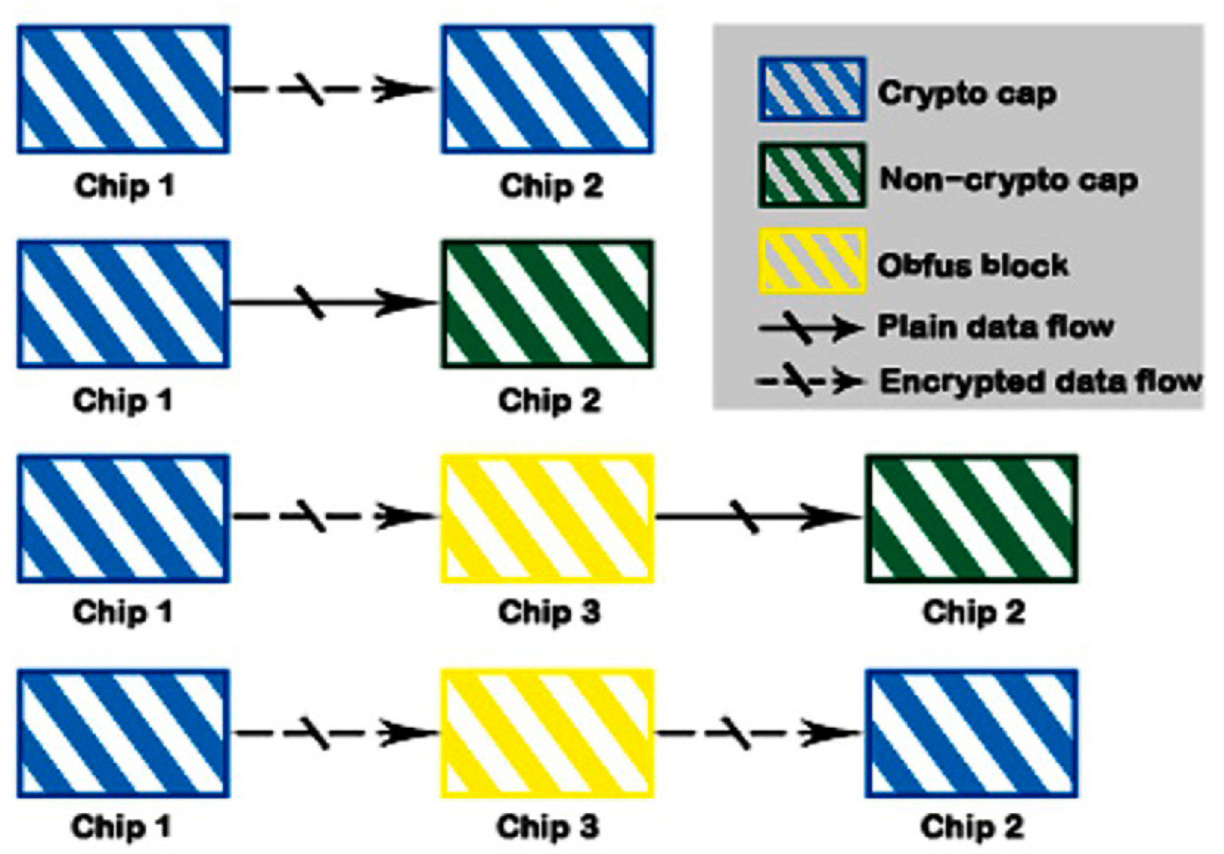
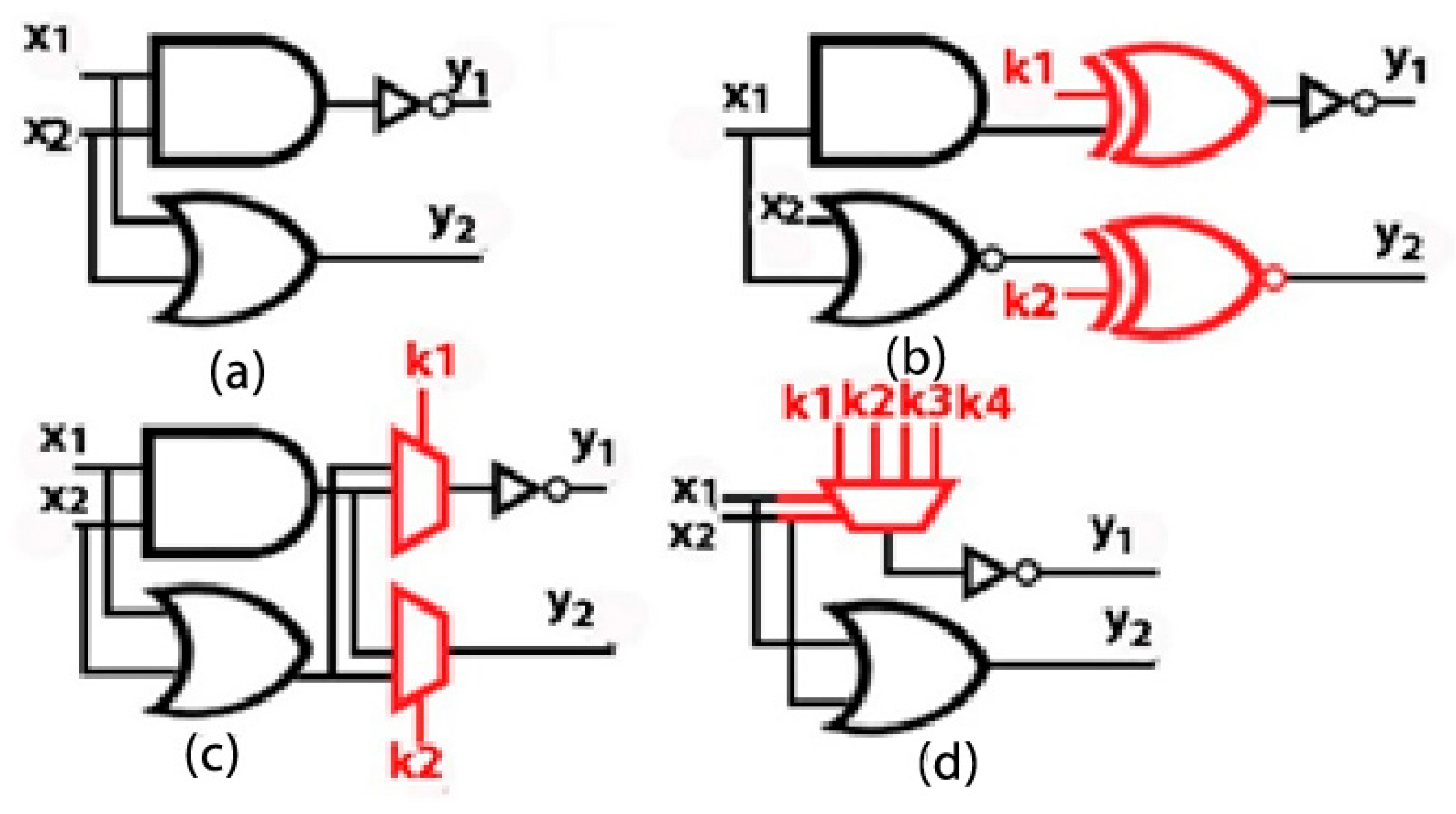
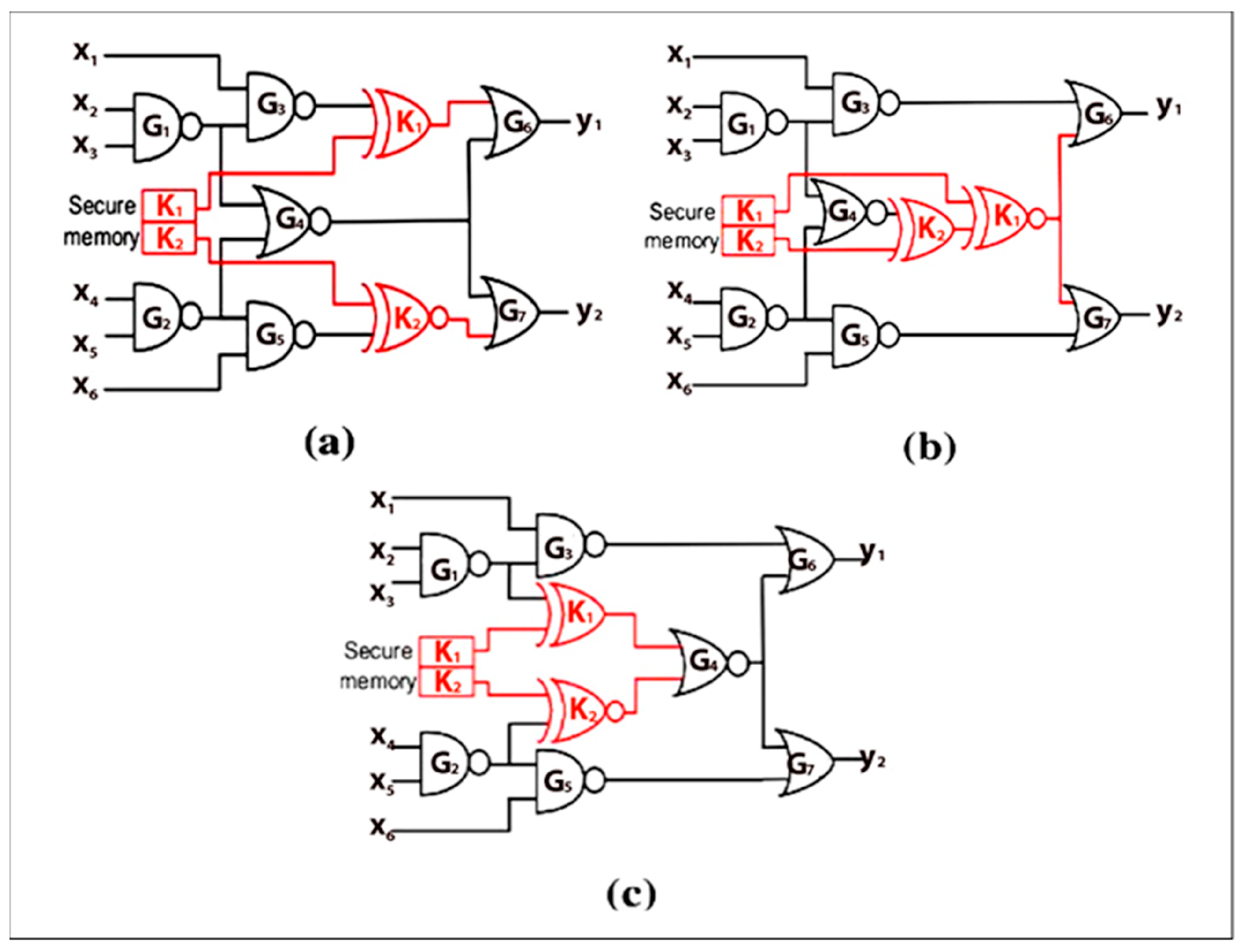
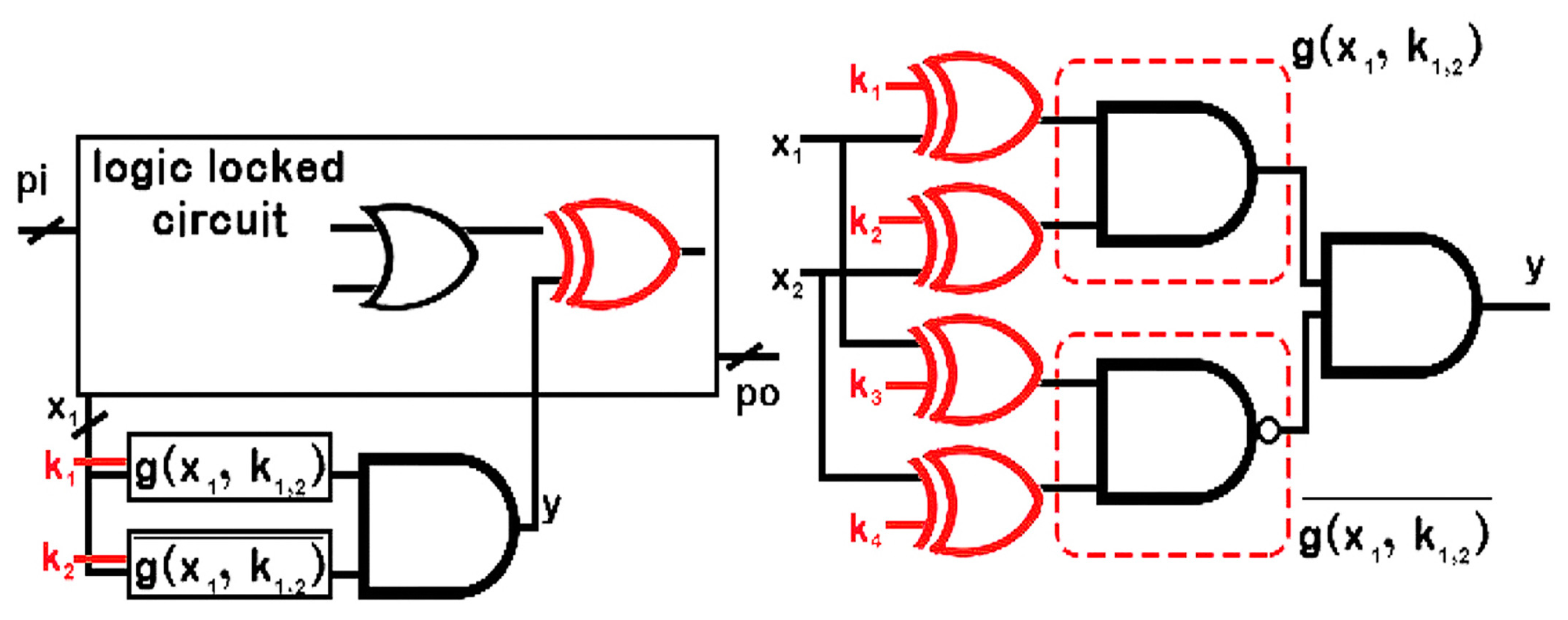
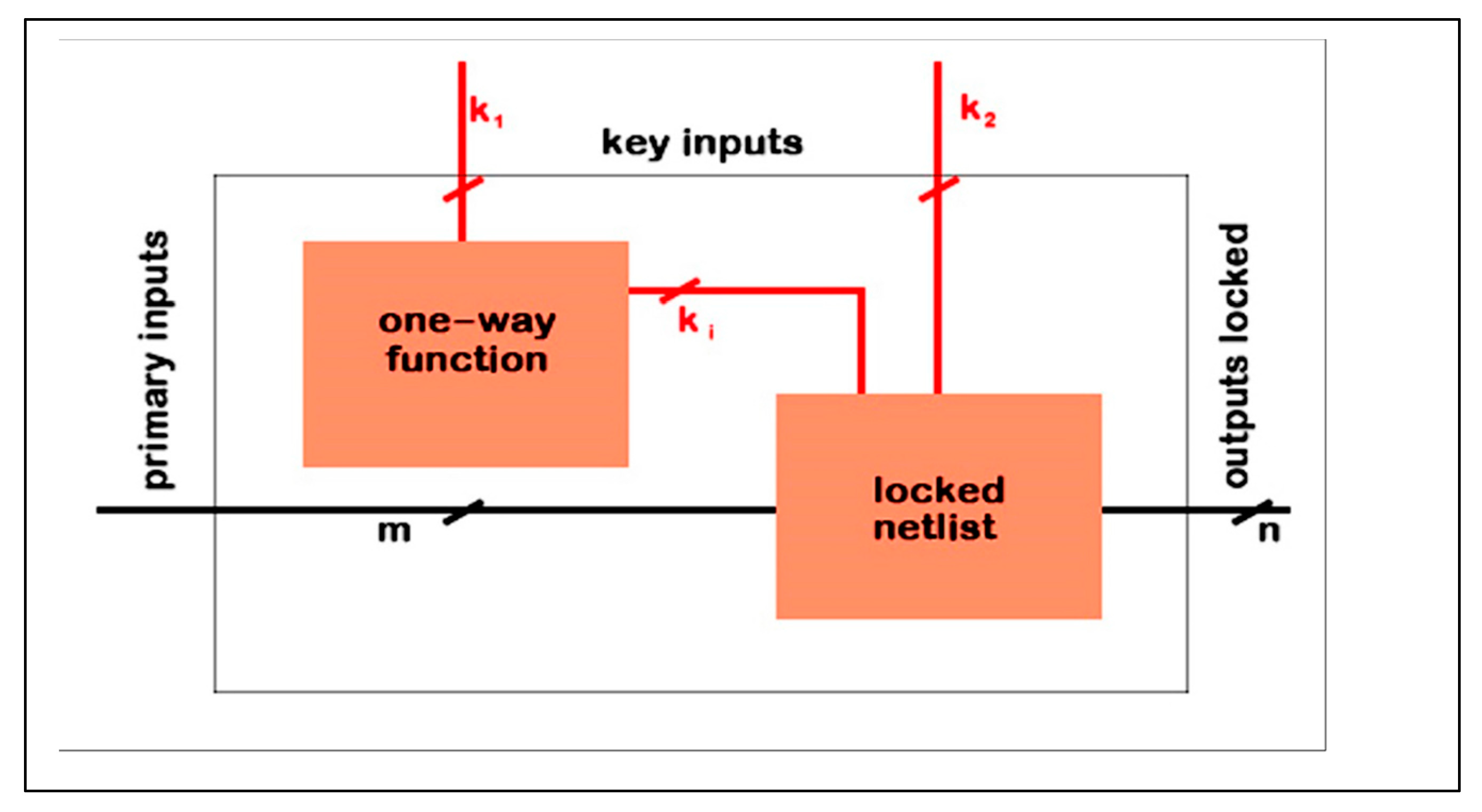
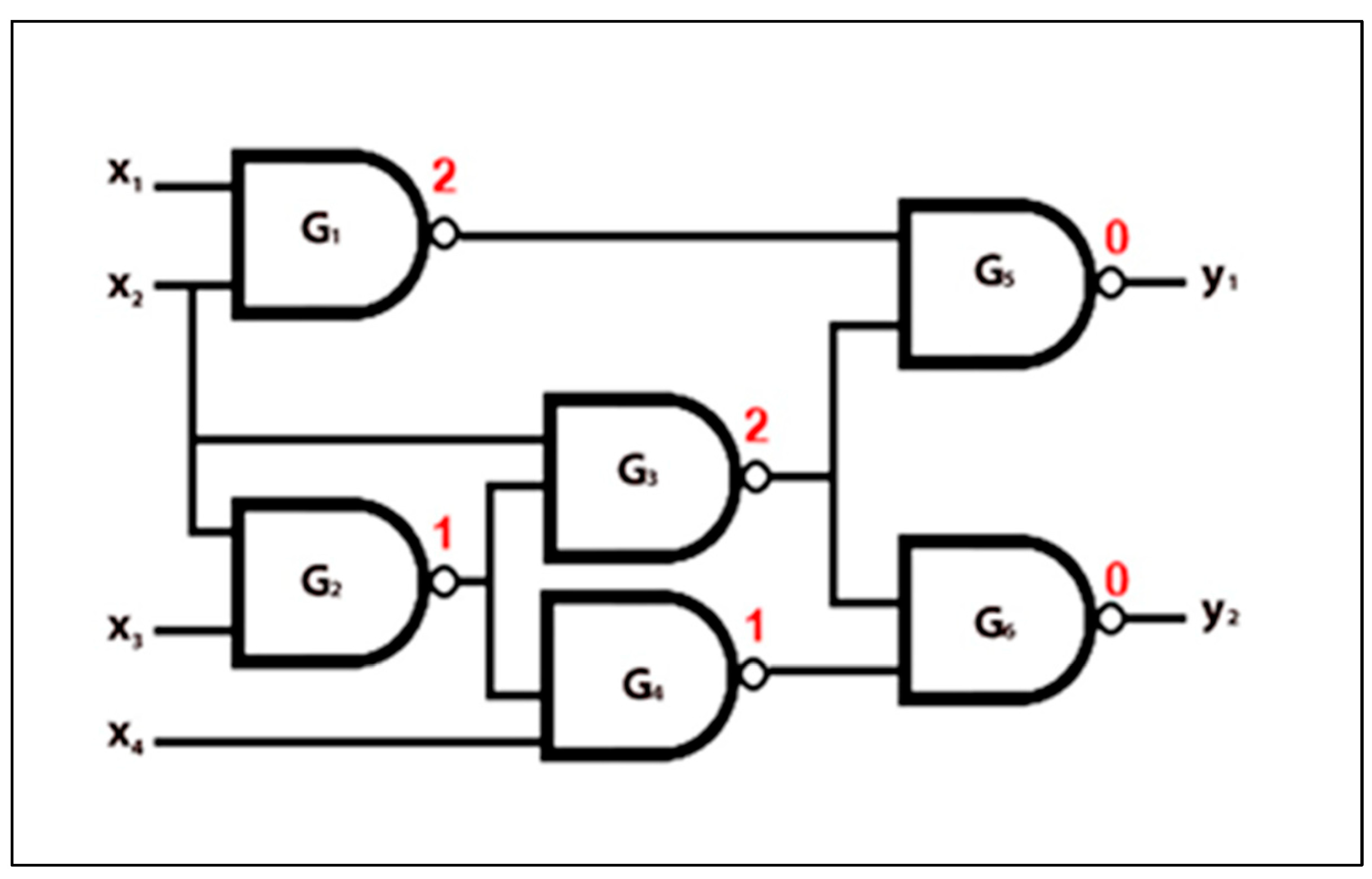
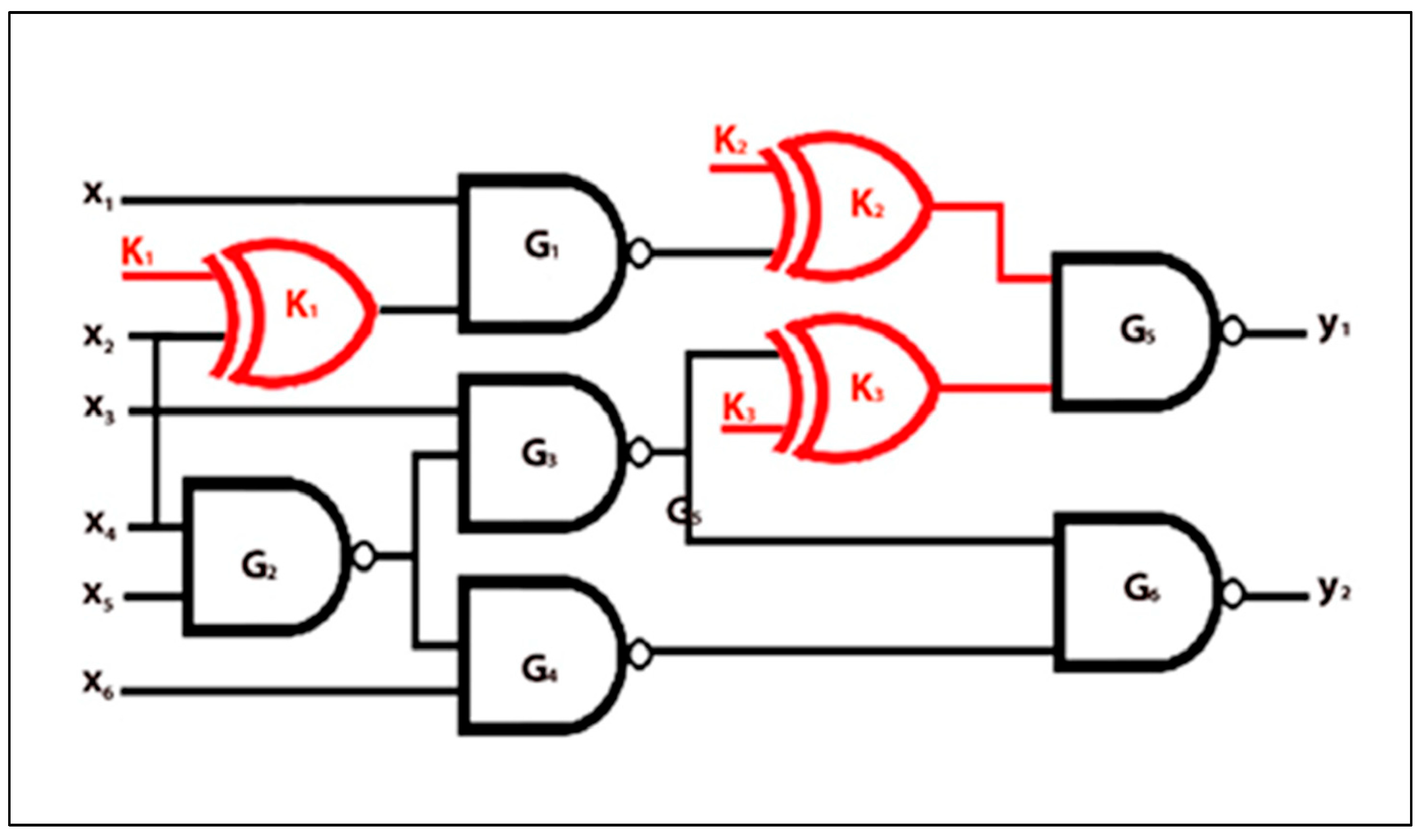
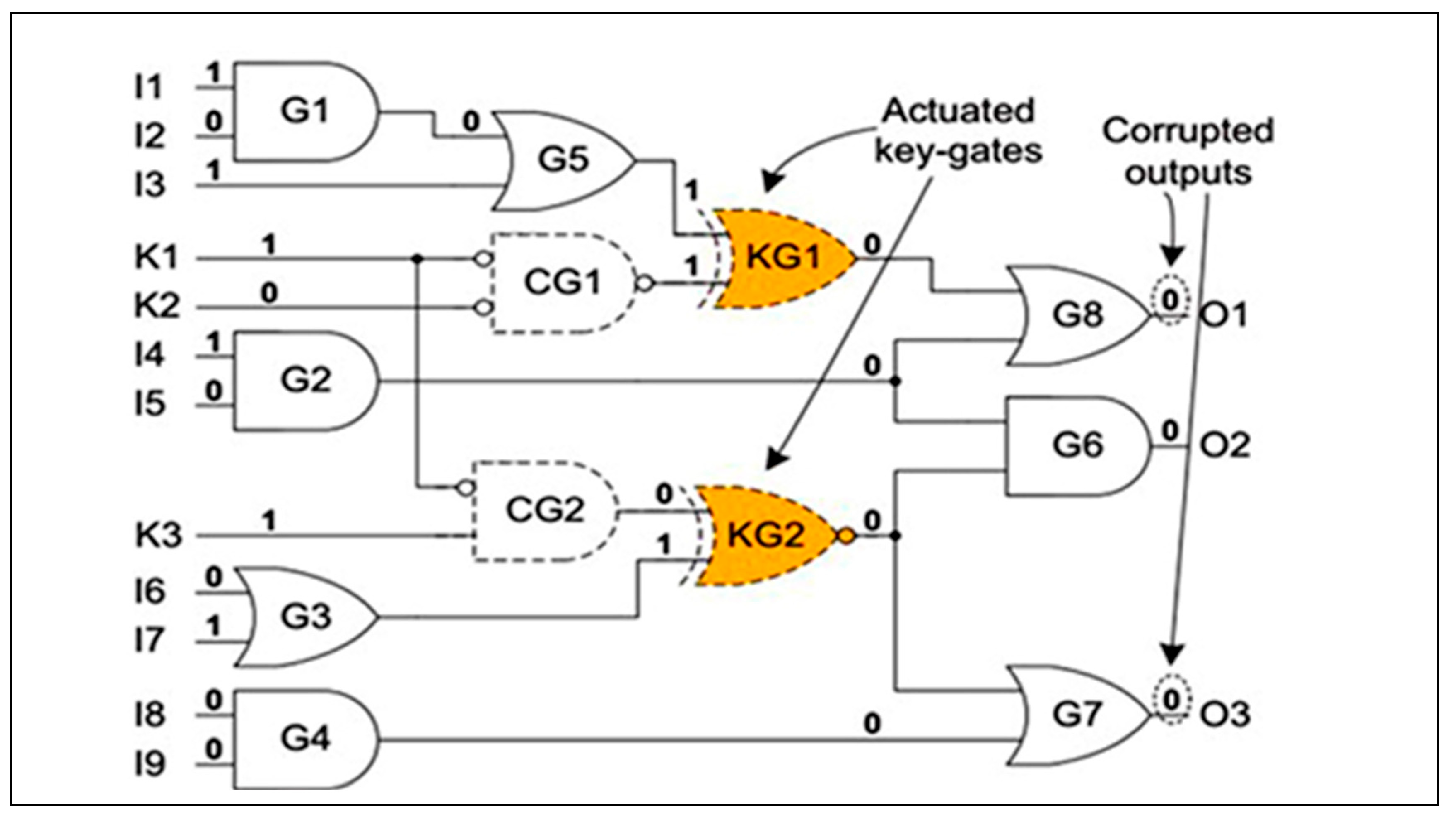
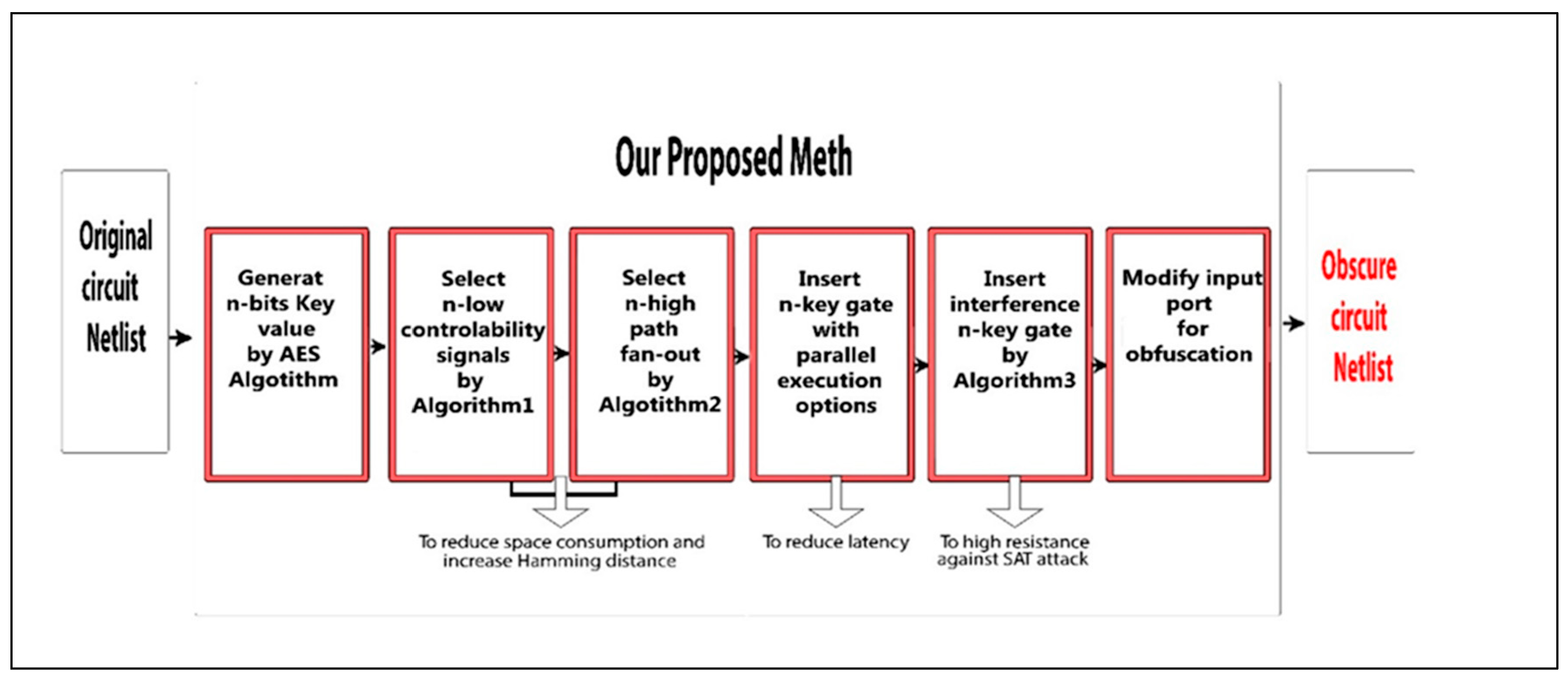
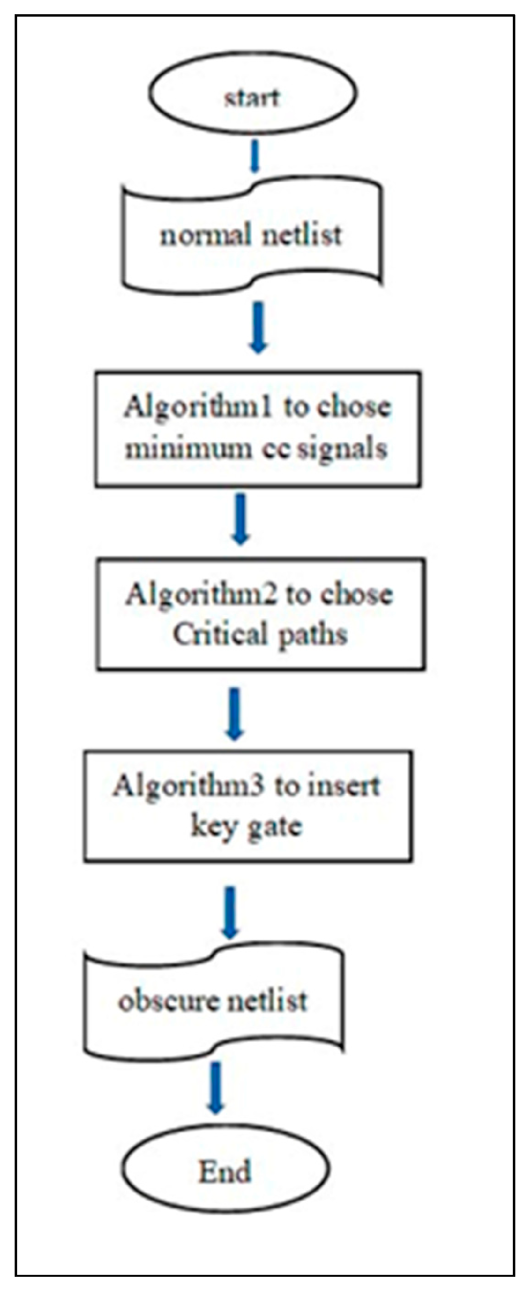
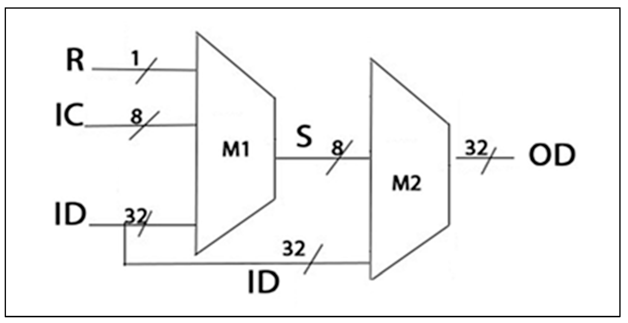
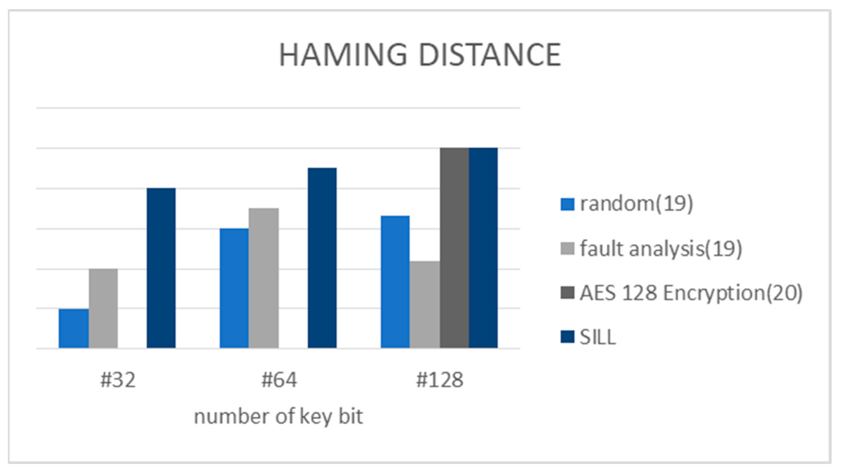
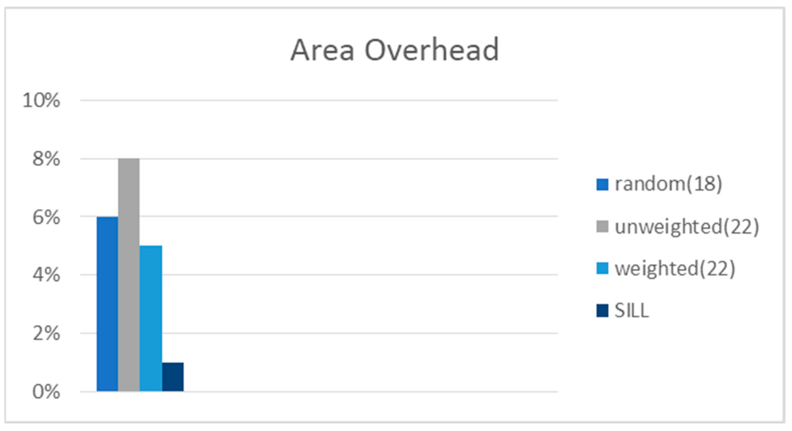
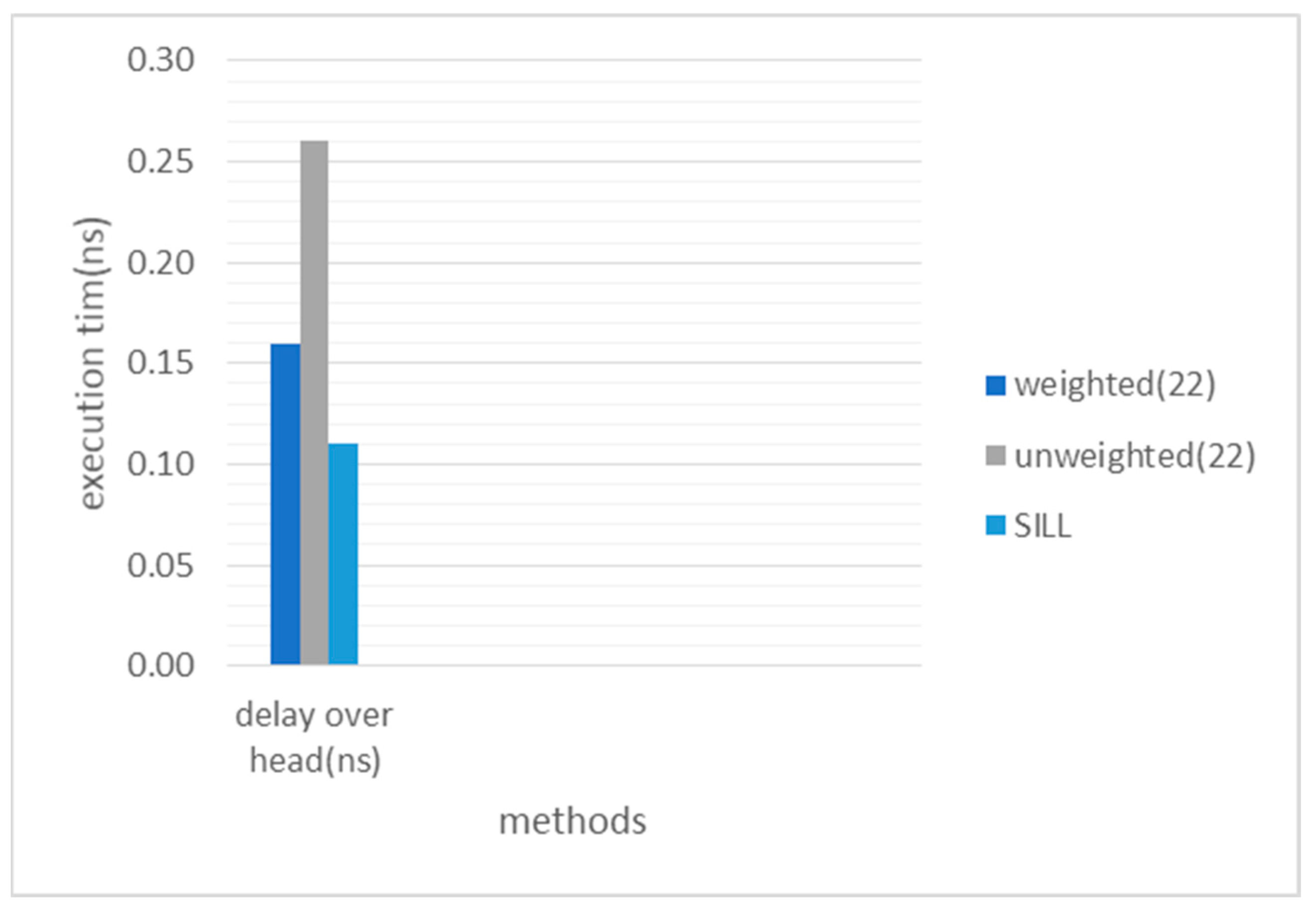