
A Novel Bidirectional-Switched-Capacitor-Based Interlaced DC-DC Converter


Abstract
:1. Introduction
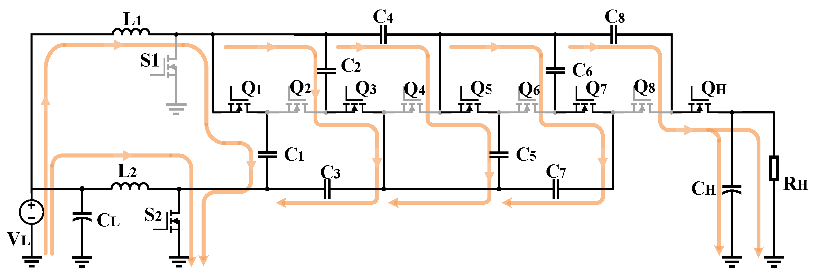
2. Circuit Topology
2.1. Main Circuit
2.2. Circuit Operation
2.2.1. The First Switching Interval
2.2.2. The Second Switching Interval
2.2.3. The Third Switching Interval
2.2.4. The Fourth Switching Interval
2.3. Switched Capacitor Circuit
3. Voltage Conversion Ratio
3.1. Ideal Case
3.2. Actual Case
3.2.1. Ripple Voltage
3.2.2. Ripple Voltages and
3.2.3. Actual Voltage Conversion Ratio in Boost Mode
3.2.4. Actual Voltage Conversion Ratio in Buck Mode
3.3. Capacitor Voltage Stress and Stored Energy
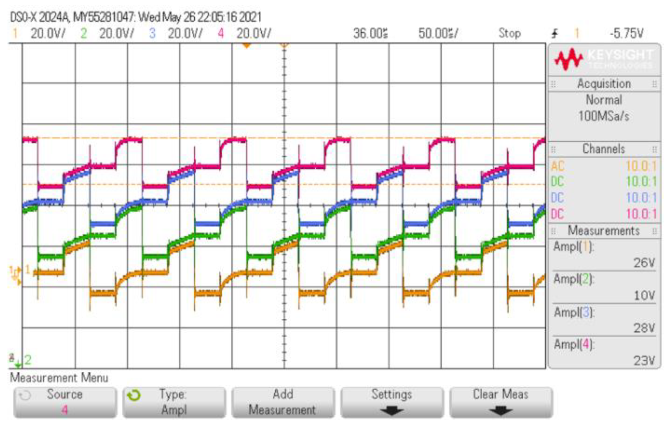
4. Experimental Results
- A.
- Boost mode
- B.
- Buck mode
5. Conclusions
Author Contributions
Funding
Data Availability Statement
Conflicts of Interest
References
- Park, S.H.; Katzir, L.; Shmilovitz, D. Reduction of Voltage Drop and Ripple in Voltage Multipliers. In Proceedings of the 2015 17th European Conference on Power Electronics and Applications, Geneva, Switzerland, 8–10 September 2015. [Google Scholar]
- Li, W.; He, X. A Family of Interleaved DC–DC Converters Deduced from a Basic Cell with Winding-Cross-Coupled Inductors (WCCIs) for High Step-Up or Step-Down Conversions. IEEE Trans. Power Electron. 2018, 23, 1791–1801. [Google Scholar] [CrossRef]
- Coutellier, D.; Agelidis, V.G.; Choi, S. Experimental Verification of Floating-Output Interleaved-Input DC–DC High-Gain Transformer-less Converter Topologies. In Proceedings of the 2008 IEEE Power Electronics Specialists Conference, Rhodes, Greece, 15–19 June 2008. [Google Scholar]
- Li, W.; He, X. An Interleaved Winding-Coupled Boost Converter with Passive Lossless Clamp Circuits. IEEE Trans. Power Electron. 2007, 22, 1499–1507. [Google Scholar] [CrossRef]
- Tseng, K.-C.; Cheng, C.-A.; Chen, C.-T. High Step–Up Interleaved Boost Converter for Distributed Generation Using Renewable and Alternative Power Sources. IEEE J. Emerg. Sel. Top. Power Electron. 2017, 5, 713–722. [Google Scholar] [CrossRef]
- Lee, S.; Kim, P.; Choi, S. High Step-Up Soft-Switched Converters Using Voltage Multiplier Cells. IEEE Trans. Power Electron. 2013, 28, 3379–3387. [Google Scholar] [CrossRef]
- Pan, C.-T.; Chuang, C.-F.; Chu, C.-C. A Novel Transformer-less Adaptable Voltage Quadrupler DC Converter with Low Switch Voltage Stress. IEEE Trans. Power Electron. 2014, 29, 4787–4796. [Google Scholar] [CrossRef]
- Roy, J.; Ayyanar, R. Sensor-Less Current Sharing Over Wide Operating Range for Extended-Duty-Ratio Boost Converter. IEEE Trans. Power Electron. 2017, 32, 8763–8777. [Google Scholar] [CrossRef]
- Zheng, Y.; Xie, W.; Smedley, K.M. A Family of Interleaved High Step-Up Converters with Diode–Capacitor Technique. IEEE J. Emerg. Sel. Top. Power Electron. 2020, 8, 1560–1570. [Google Scholar] [CrossRef]
- Cockcroft, J.D.; Walton, E.T.S. Experiments with High Velocity Positive Ions―(I) Further Developments in the method of obtaining High Velocity Positive Ions. Proc. R. Soc. A 1932, 136, 619–630. [Google Scholar]
- Dickson, J.F. On-chip High-Voltage Generation in NMOS Integrated Circuits Using an Improved Voltage Multiplier Technique. IEEE J. Solid State Circuits 1976, 11, 374–378. [Google Scholar] [CrossRef]
- Alzahrani, A.; Ferdowsi, M.; Shamsi, P. A Family of Scalable Non-Isolated Interleaved DC–DC Boost Converters with Voltage Multiplier Cells. IEEE Access 2019, 7, 11707–11721. [Google Scholar] [CrossRef]
- Müller, L.; Kimball, J.W. High Gain DC–DC Converter Based on the Cockcroft–Walton Multiplier. IEEE Trans. Power Electron. 2016, 31, 6405–6415. [Google Scholar] [CrossRef]
- Prabhala, V.A.K.; Fajri, P.; Gouribhatla, V.S.P.; Baddipadiga, B.P.; Ferdowsi, M. A DC–DC Converter with High Voltage Gain and Two Input Boost Stages. IEEE Trans. Power Electron. 2016, 31, 4206–4215. [Google Scholar] [CrossRef]
- Pulvirenti, F. 3-V Input, 70-V Output, Fully Integrated Hybrid Charge Pump. IEEE Access 2022, 10, 44062–44075. [Google Scholar] [CrossRef]
- Ballo, A.; Grasso, A.D.; Palumbo, G. A simple and effective design strategy to increase power conversion efficiency of linear charge pumps. Int. J. Circuit Theory Appl. 2019, 48, 157–161. [Google Scholar] [CrossRef]
- Ballo, A.; Grasso, A.D.; Palumbo, G.; Tanzawa, T. Linear distribution of capacitance in Dickson charge pumps to reduce rise time. Int. J. Circuit Theory Appl. 2020, 48, 555–566. [Google Scholar] [CrossRef]
- Park, S.; Yang, J.; Rivas-Davila, J. A Hybrid Cockcroft–Walton/Dickson Multiplier for High Voltage Generation. IEEE Trans. Power Electron. 2020, 35, 2714–2723. [Google Scholar] [CrossRef]


| Cockcroft–Walton | Dickson | Hybrid | |
|---|---|---|---|
| Cockcroft–Walton | Dickson | Hybrid | |
|---|---|---|---|
| Item | Reference | Rating | Part No. |
|---|---|---|---|
| Inductor | L1, L2 | 1 mH | --- |
| MOSFET | S1, S2, QH, Q1~Q8 | 200 V, 56 A, Rdson = 40 mΩ | IRFB260NPBF Infineon |
| Capacitor | C1~C8 | 6 uF, 800 V | ECW-FG80605J Panasonic |
| Capacitor | CL | 68 uF, 35 V | EEU-FR1V680 Panasonic |
| Capacitor | CH | 56 uF, 600 V | LGN2X560MELB25 Nichicon |
| Voltage Multiplier | Cockcroft–Walton | Dickson | Hybrid |
|---|---|---|---|
| Voltage gain | |||
Disclaimer/Publisher’s Note: The statements, opinions and data contained in all publications are solely those of the individual author(s) and contributor(s) and not of MDPI and/or the editor(s). MDPI and/or the editor(s) disclaim responsibility for any injury to people or property resulting from any ideas, methods, instructions or products referred to in the content. |
© 2023 by the authors. Licensee MDPI, Basel, Switzerland. This article is an open access article distributed under the terms and conditions of the Creative Commons Attribution (CC BY) license (https://creativecommons.org/licenses/by/4.0/).
Share and Cite
Shyu, K.-K.; Yu, Y.-C.; Lin, X.-L.; Lee, L.-H.; Lee, P.-L. A Novel Bidirectional-Switched-Capacitor-Based Interlaced DC-DC Converter. Electronics 2023, 12, 792. https://doi.org/10.3390/electronics12040792
Shyu K-K, Yu Y-C, Lin X-L, Lee L-H, Lee P-L. A Novel Bidirectional-Switched-Capacitor-Based Interlaced DC-DC Converter. Electronics. 2023; 12(4):792. https://doi.org/10.3390/electronics12040792
Chicago/Turabian StyleShyu, Kuo-Kai, Yi-Chang Yu, Xin-Lan Lin, Lung-Hao Lee, and Po-Lei Lee. 2023. "A Novel Bidirectional-Switched-Capacitor-Based Interlaced DC-DC Converter" Electronics 12, no. 4: 792. https://doi.org/10.3390/electronics12040792