Article

A Fully Integrated Solid-State Charge Detector with through Fused Silica Glass via Process

1
Institute of Microelectronics of the Chinese Academy of Sciences, Beijing 100029, China
2
School of Integrated Circuits, University of Chinese Academy of Sciences, Beijing 101408, China
3
Institute of High Energy Physics Chinese Academy of Sciences, Beijing 100049, China
*
Author to whom correspondence should be addressed.
Electronics 2023, 12(4), 1045; https://doi.org/10.3390/electronics12041045
Submission received: 21 December 2022 / Revised: 13 February 2023 / Accepted: 15 February 2023 / Published: 20 February 2023

Abstract

:
A charge detector is a vital component in neutrino and dark matter detection. The integration of a charge collector in the form of flat pads and readout modules has been proposed as an optimization method as it can reduce noise and installation complexity. As a substrate, fused silica glass has attracted considerable attention due to its low radioactive background properties. In this research, based on the application requirements of a high charge collection rate and low noise, the structure of the charge detector was designed using calculation and simulation methods. The entire manufacturing process is described. In addition, a novel through glass via (TGV) structure composed of a conformal metal layer and a photosensitive material that is easy to fabricate and has high morphological compatibility with via filling is proposed. The curing property of the new material was characterized. A fully integrated solid-state charge detector with 32 groups of TGVs was realized. Additionally, the electrical properties of key structures were tested and analyzed.

1. Introduction

In the field of particle physics, neutrino [1,2] and dark matter [3,4] detection usually uses the behavior of detected particles such as electrons and photons to infer the correctness of theories or hypotheses. The implementation of particle trajectory reconstruction in a TPC (time projection chamber) [2,5,6] is an advanced detection method.
Experiments in this field are characterized by difficult installation, high cost, and long working time and require high integration, stability, and detection accuracy from the collection components. For example, in neutrino detection experiments [1], crossed wires have been used to inductively count drift electrons. The span of this structure in the TPC was so large that the deflecting of the wires under gravity and an electric field affects the measurement accuracy, and a reinforcement method to solve this problem introduces a larger radioactivity burden [7]. Additionally, the individually independent nature of the wires increases both the difficulty of position reconstruction and environmental noise [8]. Moreover, in the cross-wire structure, a high voltage was loaded between the upper wires (sensing layer) and lower wires (collection layer) to increase the collection efficiency. This voltage generated a high field, which may cause discharges and electrical noise [9]. Therefore, an alternative structure for charge inductivity and collection was required.
Flat pads that can be deposited on a substrate have been proposed for their lower noise and signal loss. Furthermore, it is possible to integrate the collection layer, transport wires, and readout into three dimensions. Additionally, the integrated pads can be grounded simultaneously, eliminating calculation difficulties due to high fields. Owing to the large-scale thickness difference between the pads (can be at an nm scale) and substrate (usually at an mm scale), the introduction of large amounts of substrate material has become a major concern for low background control efforts. In TPC, and especially in neutrinoless double-beta decay experiments, 232Th, 238U, and 40K were the three primary radionuclides contained in materials that contributed to the background. As was measured in [6,10,11], Heraeus’ fused silica (referred to as “quartz” in the paper) contained less than 0.23 ppt of 232Th, well below the levels found in epoxy-based substrate (23–540 ppt, limited at the 90% confidence level), which is the main component in organic substrates, and less than 1.5 ppt of 238U, much lower than the levels found in epoxy-based substrates (44–360 ppt, limited at the 90% confidence level). The 40K contributed by fused silica was about 0.55 ppt, well below the level measured in epoxy-based substrates (930 ppb, limited at the 90% confidence level). Although the background performance of high-purity silicon is close to that of fused silica, as a semiconductor material, its insulating performance and dielectric strength are much lower than those of the latter. This will pose challenges for substrates to reduce noise and resist electrical breakdown in TPC structures characterized by strong electric fields. Therefore, fused silica is a preferred material used in particle physical detection experiments. Additionally, as a type of glass, the compatibility of fused silica with semiconductor processes makes it possible to integrate components modularly, such as detection parts and computing chips.
A prototype charge collector was fabricated on a 6-inch fused silica wafer and was tested in a TPC containing 9 kg of liquid Xenon (LXe) [7,12]. This was achieved by forming a double layer of metallic patterns on fused silica. The isolation of the bidirectional channels was accomplished by interlayer dielectric layer deposition [13]. However, the structure was only established on one side of the silica glass for the collection units. The interconnection with the readout application-specific integrated circuit (ASIC) relied on a range of surrounding auxiliary structures, such as the ceramic substrate, a large number of bonding wires, and mechanical assembly structures. It increased noise and assembly complexity on the one hand and reduced the particle collection efficiency due to the surrounding structures for the connection on the other.
To address the above problems, we introduced the TGV structure. This structure enabled electrical interconnection between the collection pads and the backside readout unit in a vertical direction.
In this article, the design and optimization of a charge detector with a high collection efficiency are presented. A novel method for filling large-diameter, high-steepness through-vias with metal and photosensitive insulating materials is described. The basic properties of the new material introduced to the TGV are characterized. A fully integrated solid-state charge detector was fabricated with TGVs on a 6-inch wafer. The resistances and capacities were tested and compared.

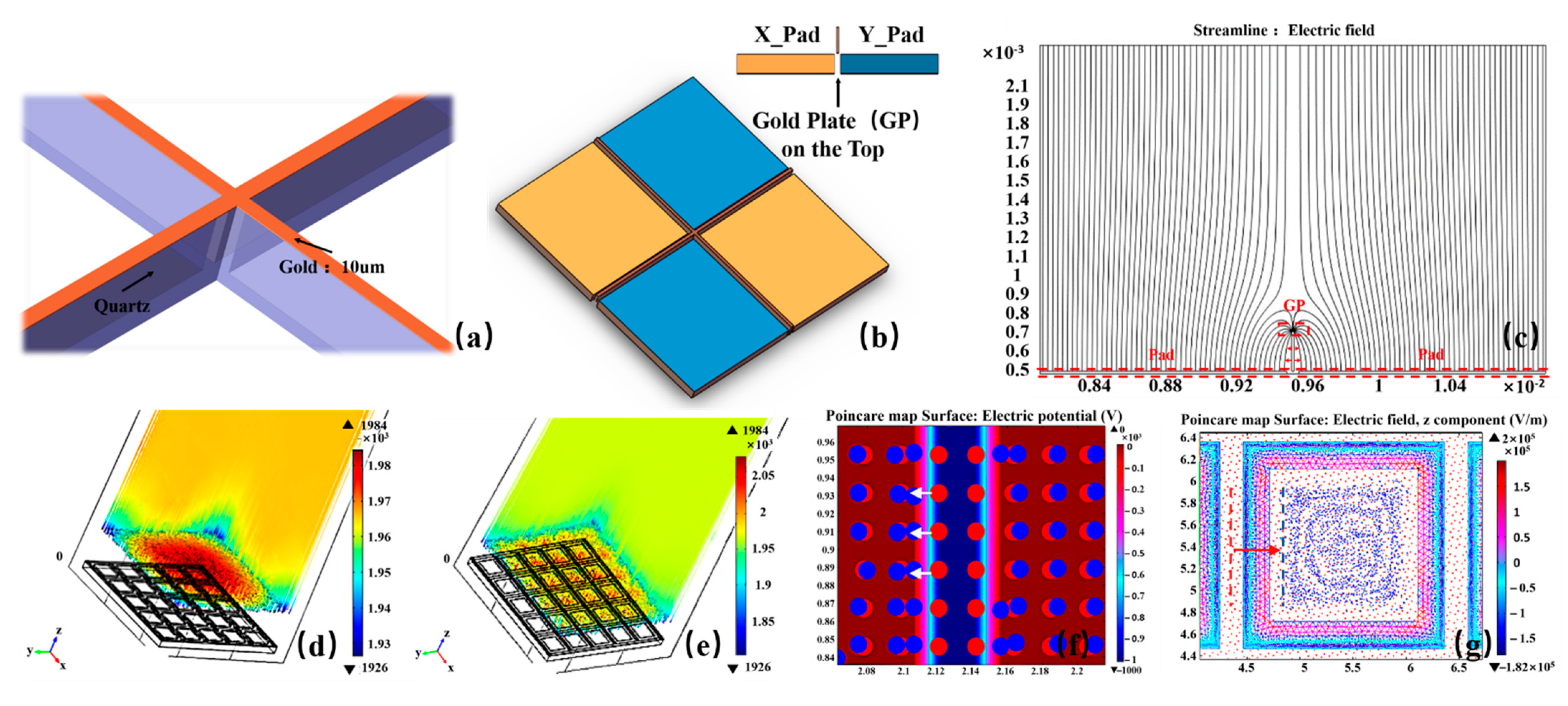
2. Structure Design and Simulation

In TPC, the design of the detector takes into account three aspects: (1) Spatial resolution. This requires that the two-dimensional (X-axis and Y-axis) decomposition of the graph be as equivalent as possible to reduce the statistical complexity of the signal. (2) Collection efficiency. It requires high coverage at an effective ratio. (3) Low crosstalk. The resistances of each strip and capacitances between channels are basic parameters that may have effects on the background discrimination of the detector. For the first factor, the smallest repeating cell selected to form the detector pattern (as shown in Figure 1) of our design should have a symmetry of 90 degrees of rotation, with adjacent graphs being equally spaced on the x and y axes when the central lines of the cells are used as axial coordinates. The effect area ratio can be expressed by the equations:
R s q = 4 a 2 ( 2 a + d ) 2
R c = π r 2 ( 2 r + s ) 2
where a and r represent half the length of the square and the radius of the circle, respectively, d and s are the minimum spacing of the two pads. The ratio of the square model is 1.3 times that of the circular model if “ a ” equals the radius of the circle “ r ” and “ d ” equals “ s ”. This indicates that the square structure in Figure 1a has a higher collection efficiency.
Next, the gap size was taken into consideration. To recover lost collection efficiency, the concept of a charge deflector was equipped on this detector (as is shown in Figure 2a,b). The deflector could be located in the gap between the pads. A tradeoff in gap size was made by the simulations.
At a distance of 50 mm from the collector, 10,000 electrons were released uniformly. The electron mobility of the liquid xenon was set to 400 cm2/(V·s), the saturation drift rate was 2 × 105 cm/s, and the bias voltage of the deflector was −100 V. The size of the collection pad was set to 2 mm, the gap width was 110 μm, and the deflector width was 70 μm, which was located in the middle of the gap. The electric field line distribution and particle drift trajectory in the TPC cavity were obtained (as shown in Figure 2), respectively. The number of electrons left on the surfaces of each structure was counted. It was 9807 on the pads, 169 on the gold plate (GP), and 5 on the gap. The collection efficiency after increasing the deflector was calculated as 98.07%, which was much higher than the 89.8% without a deflector. Therefore, in this design, the deflector assembly space was reserved, and the gap size was set to 120 μm, considering the assembly tolerance.
When balancing the contradiction between assembly and process yield, this detector set the basic unit area to 10 cm × 10 cm. Additionally, the pads were cross-linked, forming 16 X strips and 16 Y strips, to connect with a 32-channel readout chip, where the diagonal of the square in the strips was 6 mm and the gap between the two pads was 120 μm. The 32-channel digital chip was used as the readout ASIC. TGVs were arranged at the end of the strips to realize the vertical interconnection between the front-side collection strips and the back-side readout module/chip (as shown in Figure 3).

3. Fabrication Process and Tests
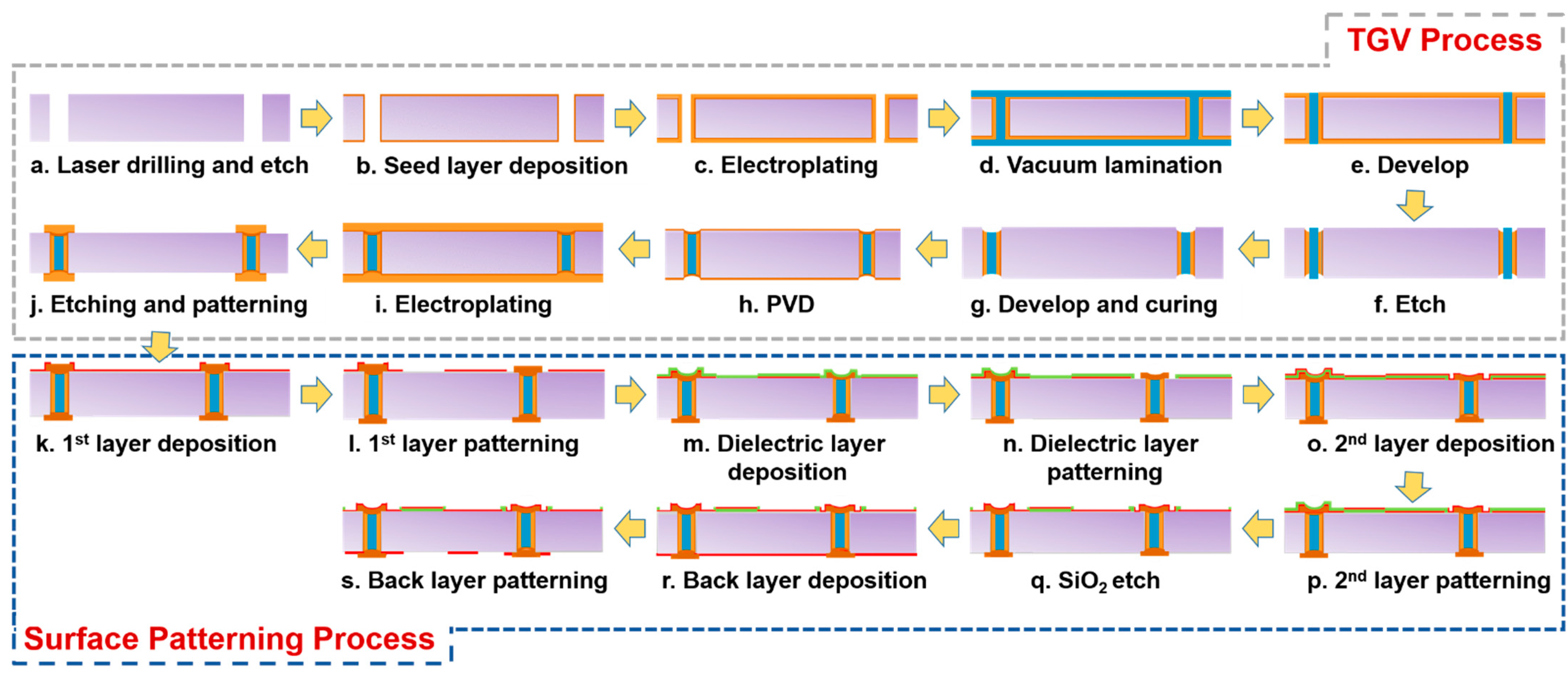
Besides the mature build-up process on the glass substrate, new challenges exist with this method. Fused silica glass, a high-purity glass, is difficult to drill and polish compared to other glass types, especially those that can be selectively doped. When the thickness of the fused silica glass substrate needs to be greater than 300 μm to achieve high roundness and consistent interconnection vias, laser drilling and wet etching are generally used to form through vias with a diameter of ≥70 μm [14,15,16]. The morphology of a via with a large diameter (≥70 um) and high depth (300–500 um) directly affects the feasibility of the metallization process. Additionally, compatibility with the subsequent process of multi-layer surface patterning has also become one of the key issues to be considered in the TGV process design [17,18].

3.1. TGV Process

In this paper, a fully filled TGV-independent structure is proposed (as shown in Figure 3). The fused silica glass substrate was drilled as the initial structure first, and the inner layer was covered with conformal metal to form the conductive path. In the middle of the via was a support structure formed with a cured photosensitive material, which was rich in silica glass particles. The chemical mechanical polishing (CMP) process was excluded to avoid the problem of tilting after double-sided via plating. Therefore, wet etching was used to remove surface metal. A pad was added at both ends of the via with a size between the via diameter and the size of detector elements to ensure full coverage of the organic material and to compensate for the pattern shifts due to alignment inaccuracies. The process flow is shown in Figure 4a–j.
The focus of this process was on via formation and via plugging technology, and the difficulty lay in the precision control in the key steps.
In terms of via formation technology, picosecond laser hole formation technology was selected to form a through-via with a diameter of about 80 µm. Under the action of a picosecond pulse, the glass produced local melting and Coulomb explosion effects. The former generated particles aggregated around the via perimeter, and the latter formed micro-cracks and small areas of chipping (as shown in Figure 5a). It affected the continuity and high adhesion of the seed layer. Therefore, ultrasonic cleaning and wet treatment were added to form a proper morphology as shown in Figure 5c. Due to the poor adhesion of copper to fused silica glass, it was necessary to increase Ti or Cr to excess.
In terms of via plugging technology, a certain thickness of the metal layer inside the via was deposited to ensure electrical interconnectivity. The application in this paper was for a small signal transmission, thus an electrical path with a sidewall thickness of about 5 µm was formed in a vertical line. Pulse current was selected, the current density was 0.1 A/dm2, and the plating time was 40 min. Then, a photosensitive material was vacuum laminated at 80 °C in a vacuum and a 0.5 MPa mechanical pressure. Then, it was heated to 100 °C to achieve the complete filling of a deep via. A roughly 30 µm-thick film was left on the surface of the substrate. Then, a horizontal line of Na2CO3 at 1 m/min was used to develop the photosensitive material. This process should be under fine control to ensure that the surface organic film is completely removed while ensuring that the filling in of the via does not develop. Subsequently, the metal on the surface was etched to expose the substrate and part of the photosensitive material.
Then, we repeated step e in Figure 4 and made sure the photosensitive material in the via was flush with or slightly below the surface. The precise control of this step of the process was particularly important. If too much of the photosensitive material was removed, a deep dimple would be created at the aperture (as shown in Figure 6a), and re-plating was required to ensure the flatness of the surface so as not to affect the multilayer patterning process. However, re-plating would increase the thickness of the metal pad on the surface, leading to the problem of poor mask coverage due to height differences in the subsequent process. However, if the photosensitive material was not removed cleanly, it would lead to insufficient adhesion of the surface metal, resulting in problems such as delamination or even peeling (as shown in Figure 6c). Next, after the formation of the internal support structure, Cr and Cu were deposited again (as shown in Figure 4h,i). Finally, a fully filled via structure without polymer exposure was obtained.
In this structure, except for the extremely thin Ti adhesion layer, there were mainly three materials: fused silica glass, copper, and photosensitive material. Inconsistent deformation, stress, sidewall spalling, surface peeling, and other reliability issues exist between the copper and fused silica glass due to the coefficient of thermal expansion (CTE) mismatches in the structure when it is processed at high temperatures or used at ultra-low temperatures. Therefore, TAIYO INK SR3 with an intermediate CTE and a relatively low Poisson’s ratio (shown in Table 1) was selected as the support structure in this model. SR3 can play a role in reconciling the reliability problems caused by the thermal mismatch between fused silica glass and copper.
There are two kinds of sensitizers in the uncured SR3 material, one of which needs to be processed by exposure to form a cross-linking polymer, and the other of which needs to be heated to form a bonding polymer with an aromatic solvent to achieve curing (as shown in Figure 7).
The properties of SR3 depend on its degree of cure. Both the unsaturated bonds and processed products lead to changes in material properties due to their instability, thereby affecting structural reliability. Thus, in this paper, a thermo-gravimetric analysis was performed to determine the effect of different conditions on its degree of cure.

3.2. Charge Detector Integration Process

Figure 4k–s shows the whole process flow of the detector integration. TGV was fabricated at one end of each strip. Ti was sputtered on as an adhesion layer. Then, a 500 nm-thick gold layer was sputtered on with physical vapor deposition (PVD). SiO2 was deposited between two metal layers as a bridge for insulating two strips with low-pressure chemical vapor deposition (LPCVD) [7,12]. The thickness of this dielectric layer was 1 µm. Additionally, SiO2 on the first pattern layer was etched with inductively coupled plasma (ICP) until the other processes were completed on the front side. Finally, a fan-in pattern was fabricated on the backside while bonding the front side to a holder.

3.3. Tests

3.3.1. Material Characterization

SR3 is a new material that has never before been used in vias. Its physical and mechanical properties are greatly dependent on the degree of cure, and this is extremely important for the later process while the thermal cycle and the temperature shock load onto this structure, which might cause failure. Differential scanning calorimetry (DSC) is one of the most important techniques for the analysis of the curing degree. It has a procedure that allows for an accurate determination of the melting enthalpy (or the degree of crystallinity) of polymer materials. An obvious peak with transitions in materials as a function of temperature or time in a controlled atmosphere can be observed if the detected substance has physical or chemical changes. According to the principle of polymerization, three steps may affect the curing degree of SR3; the steps are exposure, ultraviolet (UV) irradiation, and heating. In this research, group experiments were designed to elucidate the effect of different conditions on curing.

3.3.2. Electrical Properties Tests

This structure is based on the potential difference generated after the electrons are detected on the surface and transmitted to the back ASIC to realize the identification of particles after signal extraction and processing. Therefore, in a small-signal transmission system with a limited number of particles, the structure requires the minimization of the channel resistance, the adjacent-channel capacitance, and the cross-channel insulation. The four-probe test method was chosen to demonstrate an accurate resistance value, especially of the TGV. An ATG S2-8CF with a Kelvin A3A101821KS probe was used as the test equipment. It can realize a test of 0.25 mohm to 1 kohm, and the accuracy is 0.025 mohm. Meanwhile, the embedded capacitance test was designed for capacitance testing. The capacitance test coverage ranges from 0.1 pF to 100 mF, and the accuracy is 0.03 pF. Two charge detectors with TGV were selected for electrical performance tests. Among them, the 1st piece was a sample that was completed in the first batch, and the second was achieved in the second batch.

4. Results and Discussion

4.1. Charge Detector with TGV

A good charge detector prototype with TGV was achieved, which is shown in Figure 8. The bright colors on the edge of the pattern are the TGVs covered by a small pad (shown in Figure 9b). A total of 32 small pads were connected to each strip. A fan-in structure was designed to introduce the outer large pads covered on the TGV to the inner small pads, which were prepared for wire bonding with the test board.
The TGV structure shown in Figure 9 was formed. The thickness of the conformal metal layer was about 6 µm, the metal continuity in the via was good, the thickness of the surface pad metal was about 11 µm, and the height of the dish was less than 6 µm. Figure 9b shows a top view of the small pad after the whole process.
It can be observed that the edge of the pad had good continuity, and the metal in the non-pad area had no climbing structure. Thus, we can infer that the thickness of the surface pad did not affect the climbing ability during the polymer coating process or the cleaning ability of the photoresist on the edge during development. In addition, there was neither polymer residue nor subsequent metal deposition in the dish area of the via. Therefore, it can be concluded that the removal effect of the photoresist was good under the condition of the dish depth. This dimensional difference can be used as a limiting condition, and thus, in the future, we should explore the influence of the ratio of conformal metal thickness to SR3 volume on the structural performance and reliability.

4.2. SR3 Characterization

The peak of every curve in Figure 10 represents an exothermic state, which can be used to measure the reaction ratio by comparison with the heat flow value of the uncured sample. It can be seen from the second and fourth samples that the exposure and UV methods had the same effect on the reaction ratio. Heat had the greatest effect among the three conditions. Unlike the others, the heat flow curve of the fifth sample does not show any obvious fluctuation.
Whether in the pre-cured or fully cured state, it can be observed from the figure that the heat flow curve began to show a trough after 250 °C, indicating that SR3 gradually entered a molten state. Therefore, the downstream process should be controlled under low-temperature conditions to match the tolerance of this structure. For the silicon nitride deposition process in particular, we chose the low-pressure chemical vapor deposition (LPCVD) process with a temperature of about 200 °C to ensure the reliability of the TGV structure.

4.3. Electrical Properties of the Charge Detector

The resistances of strips, vias, wires on the backside, and channels were measured, respectively (shown in Figure 11a–e). As can be seen, the processing consistency of the second prototype is significantly higher than that of the first prototype. This is because the second prototype was achieved through an optimization process after the first batch of the first prototype. In the second batch of the optimization process, a cleaning process was added to ensure cleanliness. The operation time of each process and the interval time between processes were tightly controlled in the second batch. In addition, the first sample was reprocessed during the X-strips layer processing due to staining, thus the resistance value is significantly higher. Other strip resistances were stably controlled from 14 to 26 ohms. All TGVs were at the milliohm scale, which had little effect on the total resistance value, but it can be inferred that there are invalid ones among the five vias in the channel with a larger resistance value. The main reason for the difference was that the length of the lines on the back were different. The resistance range of the back-side wires was 1 to 5 ohms.
Additionally, probes touched one end of each of the two adjacent strips, respectively. A fixed frequency of 1 MHz and a small voltage were loaded by voltage sweep to measure the capacitance. Groups of adjacent capacitance values were selected on each of the two tiles for statistics, and the numerical distribution diagrams are shown in Figure 11f. The capacity range of the adjacent strips on the detector was 5.8 to 10.6 pF. Additionally, two pads on cross strips were randomly selected for their cross capacitance values. The values were distributed between 0.1 and 0.2 pF. This means that the capacity of each cross was 0.1–0.2 pF. Therefore, it can be inferred that the capacitance value of each strip relative to another layer of metal was about 1.6 to 3.2 pF.

5. Conclusions

In this work, a solid-state charge detector was designed to give a high collection ratio of particles and low noise in signal acquisition. Silica glass was proposed as a substrate, and the whole process of detector fabrication was described. A novel filling method of through fused silica glass via was realized. The method utilized a photosensitive material to fill in the via and solved the filling requirement on a substrate with a large diameter and high-aspect-ratio vias. It provided a solution for realizing simultaneous filling on the same substrate with different diameters. In addition, the method exposed the substrate and formed full metal coverage at the opening without subsequent CMP, which retained the high flatness and low roughness of the substrate. Meanwhile, the surface of the formed structure had no organic residue and could be used in fields with special requirements for a low background or bare materials, such as high-energy particle detection or medical treatment.
The main conclusions are described below:
(1)
A 10 cm × 10 cm collector was designed consisting of a square flat pad with a diagonal length of 6 mm and a gap of 120 µm, which was integrated on a silica glass substrate with vias connected vertically to the readout module.
(2)
Novel TGVs at the wafer level were fabricated with conformal copper and SR3 for full filling. This structure had a restriction during the subsequent processing by which the maximum temperature was required to be lower than 250 °C to achieve good reliability.
(3)
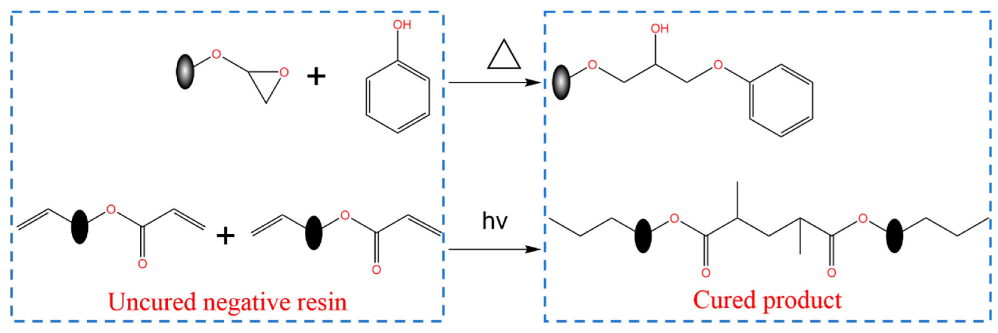
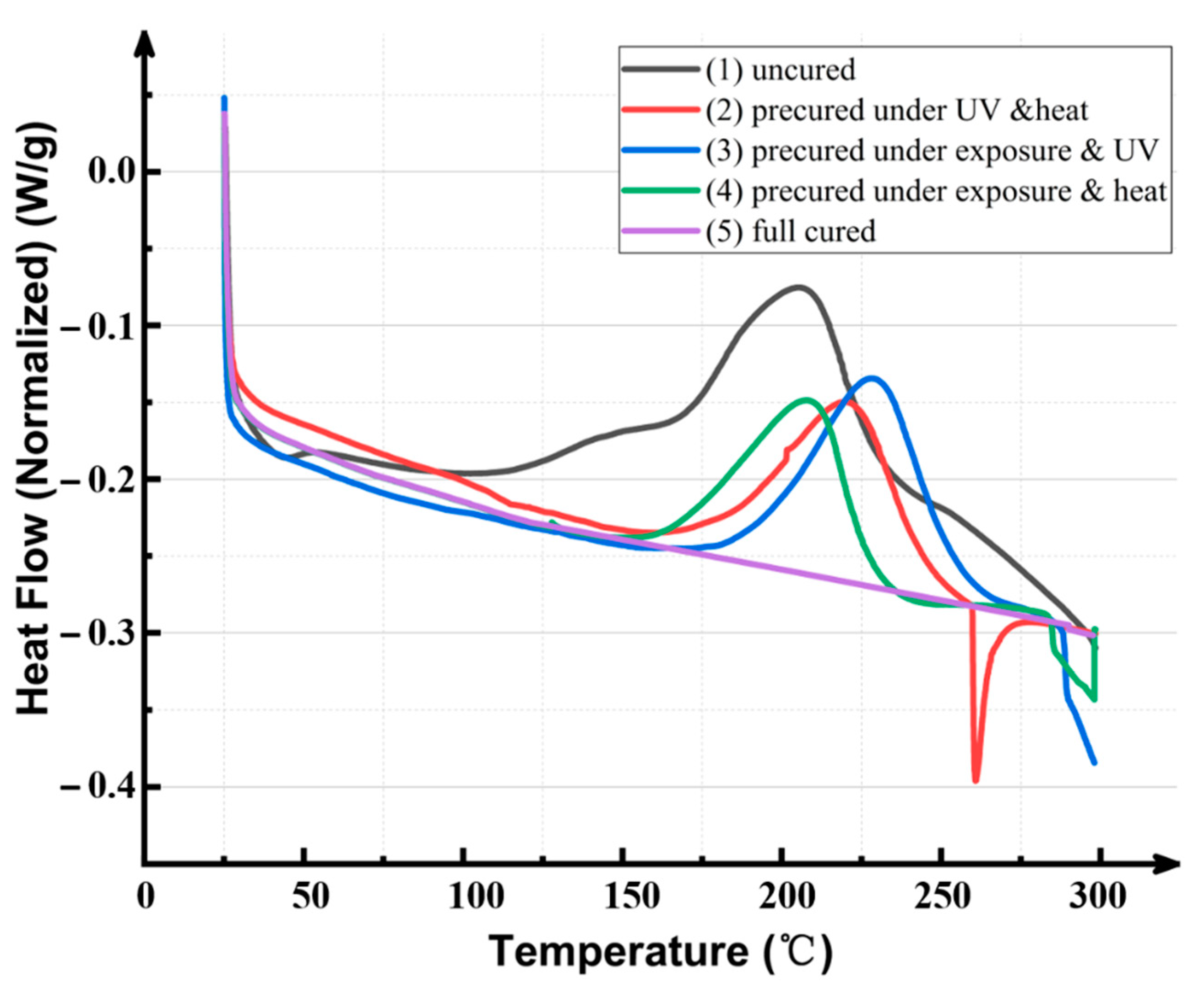
SR3, a material introduced for structural support, was characterized for its curing properties. It could be fully cured after exposure to LDI, UV, and heat baking.
(4)
Detectors with TGVs were fabricated on a 6-inch wafer. There were 32 channels with square cells. The resistance of each channel was about 15 to 31 ohm, while the resistance of the TGVs was less than 30 mohm. The capacities of the adjacent and cross channels were less than 11 pF and 4 pF, respectively.
(5)
The noise introduced by certain structural and electrical characteristics has been analyzed in [13]. Additionally, as reported in [5], the background contributions of our prototype (which was called “charge tile backing”) was below 1% single-site counts/(FWHM·2000 kg). The prototype will be installed in an experimental TPC for further testing. Although SR3 is covered and present in very small amounts, the radioactivity it introduces is also being evaluated. In addition, work on the optimization of the TGV all-copper filling process and charge deflector fabrication are in progress.

Author Contributions

Conceptualization, X.W., Q.W., L.W., L.C., and G.C.; investigation, X.W., Q.W., and G.L., package structure design, X.W., Q.W., L.W., Z.Y., and Y.F.; fabrication, X.W. and Z.F.; test and analysis, X.W., Q.W., Y.F.; writing—original draft preparation, X.W.; writing—review and editing, X.W., L.W., and Q.W.; supervision, Q.W. and L.C.; project administration, Q.W. and L.W. All authors have read and agreed to the published version of the manuscript.

Funding

This research was funded by the National Natural Science Foundation of China, grant number 11820101005.

Conflicts of Interest

The authors declare no conflict of interest.

References

  1. Auger, M.; Auty, D.J.; Barbeau, P.S.; Bartoszek, L.; Baussan, E.; Beauchamp, E.; Benitez-Medina, C.; Breidenbach, M.; Chauhan, D.; Cleveland, B.; et al. The Exo-200 Detector, Part I: Detector Design and Construction. J. Instrum. 2012, 7, P05010. [Google Scholar] [CrossRef] [Green Version]
  2. Al Kharusi, S.; Alamre, A.; Albert, J.B.; Alfaris, M.; Anton, G.; Arnquist, I.J.; Badhrees, I.; Barbeau, P.S.; Beck, D.; Belov, V.; et al. Nexo Pre-Conceptual Design Report. arXiv 2018, arXiv:1805.11142. [Google Scholar]
  3. Aprile, E.; Aalbers, J.; Agostini, F.; Alfonsi, M.; Amaro, F.D.; Anthony, M.; Antunes, B.; Arneodo, F.; Balata, M.; Barrow, P. The Xenon1t Dark Matter Search Experiment. arXiv 2012, arXiv:1206.6288v1. [Google Scholar]
  4. Vaitkus, A. R11410-22 Photomultiplier Tube Performance in the Lux-Zeplin (Lz) Experiment. In Proceedings of the APS, New York, NY, USA, 9–12 April 2022. [Google Scholar]
  5. Hilke, H.J. Time Projection Chambers. Rep. Prog. Phys. 2010, 73, 116201. [Google Scholar] [CrossRef]
  6. Adhikari, G.; Al Kharusi, S.; Angelico, E.; Anton, G.; Arnquist, I.J.; Badhrees, I.; Bane, J.; Belov, V.; Bernard, E.P.; Bhatta, T. Nexo: Neutrinoless Double Beta Decay Search Beyond 1028 Year Half-Life Sensitivity. Nucl. Part. Phys. 2021, 49, 015104. [Google Scholar] [CrossRef]
  7. Jewell, M.; Schubert, A.; Cen, W.; Dalmasson, J.; DeVoe, R.; Fabris, L.; Gratta, G.; Jamil, A.; Li, G.; Odian, A.; et al. Characterization of an Ionization Readout Tile for Nexo. J. Instrum. 2018, 13, P01006. [Google Scholar] [CrossRef] [Green Version]
  8. Albert, J.B.; Anton, G.; Badhrees, I.; Barbeau, P.S.; Bayerlein, R.; Beck, D.; Belov, V.; Breidenbach, M.; Brunner, T.; Cao, G.F.; et al. Search for Neutrinoless Double-Beta Decay with the Upgraded Exo-200 Detector. Phys. Rev. Lett. 2018, 120, 072701. [Google Scholar] [CrossRef] [PubMed] [Green Version]
  9. Jewell, M. Search for Neutrinoless Double Beta Decay with Exo-200 and Nexo; Stanford University: Standford, CA, USA, 2020. [Google Scholar]
  10. Leonard, D.; Grinberg, P.; Weber, P.; Baussan, E.; Djurcic, Z.; Keefer, G.; Piepke, A.; Pocar, A.; Vuilleumier, J.-L.; Akimov, D.; et al. Systematic Study of Trace Radioactive Impurities in Candidate Construction Materials for Exo-200. Nucl. Instruments Methods Phys. Res. Sect. A Accel. Spectrometers Detect. Assoc. Equip. 2008, 591, 490–509. [Google Scholar] [CrossRef] [Green Version]
  11. Albert, J.B.; Anton, G.; Arnquist, I.J.; Badhrees, I.; Barbeau, P.; Beck, D.; Belov, V.; Bourque, F.; Brodsky, J.P.; Brown, E. Sensitivity and Discovery Potential of the Proposed Nexo Experiment to Neutrinoless Double-Β Decay. Physical Review C 2018, 97, 065503. [Google Scholar] [CrossRef] [Green Version]
  12. Cen, W.-R.; Wu, X.-M.; Cao, L.-Q.; Wang, Q.-D.; Wen, L.-J. Novel Fused-Silica Charge Detection Tile for Particle Detectors. Radiat. Detect. Technol. Methods 2019, 3, 12. [Google Scholar] [CrossRef]
  13. Li, Z.; Cen, W.; Robinson, A.; Moore, D.; Wen, L.; Odian, A.; Al Kharusi, S.; Anton, G.; Arnquist, I.; Badhrees, I.; et al. Simulation of Charge Readout with Segmented Tiles in Nexo. J. Instrum. 2019, 14, P09020. [Google Scholar] [CrossRef] [Green Version]
  14. Yole. Glass Substrate Trend for Semiconductor Devices and Advanced Packaging Application. 2020, pp. 1–16. Available online: https://s3.i-micronews.com/uploads/2020/09/Santosh-Kumar-Principal-Analyst-Yole-D%C3%A9veloppement-SYNAPS-2020.pdf (accessed on 30 September 2020).
  15. Huang, H.; Yang, L.-M.; Liu, J. Micro-Hole Drilling and Cutting Using Femtosecond Fiber Laser. Opt. Eng. 2014, 53, 051513. [Google Scholar] [CrossRef]
  16. Kiyama, S.; Matsuo, S.; Hashimoto, S.; Morihira, Y. Examination of Etching Agent and Etching Mechanism on Femotosecond Laser Microfabrication of Channels inside Vitreous Silica Substrates. J. Phys. Chem. C 2009, 113, 11560–11566. [Google Scholar] [CrossRef]
  17. Shorey, A.; Cochet, P.; Huffman, A.; Keech, J.; Lueck, M.; Pollard, S.; Ruhmer, K. Advancements in Fabrication of Glass Interposers. In Proceedings of the 2014 IEEE 64th Electronic Components and Technology Conference (ECTC), Lake Buena Vista, FL, USA, 27–30 May 2014; pp. 20–25. [Google Scholar]
  18. Liu, Z.; Fu, H.; Hunegnaw, S.; Wang, J.; Merschky, M.; Magaya, T.; Mieno, A.; Shorey, A.; Kuramochi, S.; Akazawa, M.; et al. Electroless and Electrolytic Copper Plating of Glass Interposer Combined with Metal Oxide Adhesion Layer for Manufacturing 3d Rf Devices. In PIn Proceedings of the 2016 IEEE 66th Electronic Components and Technology Conference (ECTC), Las Vegas, NV, USA, 31 May–3 June 2016. [Google Scholar]
Figure 1. Highly symmetrical structural design for detector pads. (a) is a symmetric structure composed of square cells. (b) is a symmetric structure composed of circle cells.
Electronics 12 01045 g001
Figure 2. Design and simulation for cells of the detector. (a) is a part of a deflector. (b) is a square cell with a deflector. (c) is the electric field distribution after loading bias voltage on the gold plate of the deflector. The particles at the top are expected to be deflected by the electric field and eventually fall onto the detector pads. (d,e) are the particle distribution maps at 24 ns and 24.6 ns after the release, respectively. In (f,g), the blue dots are the particle locations where the particles follow the electric field lines and drift to the surface of the bottom detector pads and the red dots are the particle locations of the initial release at the top. In (f), it can be seen that the electrons at the top are collected at the edge of the detector pads due to the deflected electric field generated by the shielding plate. (g) shows the collection effect after the optimization of the structure and electric field.
Electronics 12 01045 g002
Figure 3. Schematic drawing of the prototype charge detector.
Electronics 12 01045 g003
Figure 4. Process flow of charge detector fully integrated with silica glass via.
Electronics 12 01045 g004
Figure 5. Processes of via formation. (a) is the morphology after picosecond laser drilling. (b) is the observed picture after ultrasonic cleaning and wet etching. (c) is a topographic picture after complete wet etching. It can be observed that after seed layer sputtering, the metal fits well with the sidewall and there is a strong continuity of the metal.
Electronics 12 01045 g005
Figure 6. Fine-controlled via plugging process. (a) is a deep dimple on the surface after filling the via caused by excessive development. (b) is a near-flat orifice stat, which formed due to a finely controlled via plugging process. (c) is an example of an unclean development process that led to peeling. There are residual particles of the photosensitive material on the fused silica glass surface, resulting in poor interfacial bonding. (d) shows good bonding on the interface between the fused silica glass and metal after a finely controlled via plugging process.
Electronics 12 01045 g006
Figure 7. Reaction of fully cured SR3.
Electronics 12 01045 g007
Figure 8. Detector prototype with TGVs.
Electronics 12 01045 g008
Figure 9. TGV details. (a) is a cross-section of the via TGV structure filled with metal and SR3. (b) is a group of TGVs for one strip covered by a small pad.
Electronics 12 01045 g009
Figure 10. Heating value by different curing conditions measured by DSC on SR3.
Electronics 12 01045 g010
Figure 11. Electrical properties of charge detectors. (a,b) are the resistance of strips from one end to the other of the detector structure on the front side. (c) is the resistance of TGV with conformal copper. (d) is the resistance value of the back-side wires. (e) is the total resistance of each channel. (f) is the capacity of adjacent strips shown in pink and the capacity of pads on two cross strips shown in blue. (g) is a photograph taken during the electrical test.
Electronics 12 01045 g011
Table 1. Specifications of the materials.
PropertiesSR3Fused Silica GlassCopper
Coefficient of thermal expansion (ppm)150.5517.7
Elastic modulus (GPa)14.373117
Elongation (%)3231
Poisson ratio0.370.170.36
Dielectric constant Er @ 1 GHz3.53.8-
Specific heat (kJ/kg K)0.930.740.39
Disclaimer/Publisher’s Note: The statements, opinions and data contained in all publications are solely those of the individual author(s) and contributor(s) and not of MDPI and/or the editor(s). MDPI and/or the editor(s) disclaim responsibility for any injury to people or property resulting from any ideas, methods, instructions or products referred to in the content.

