Article

A Monostable Physically Unclonable Function Based on Improved RCCMs with 0–1.56% Native Bit Instability at 0.6–1.2 V and 0–75 °C

by
Riccardo Della Sala
1,
Davide Bellizia
2,
Francesco Centurelli
1 and
Giuseppe Scotti
1,*
1
DIET Department, Sapienza University of Rome, 00184 Roma, Italy
2
Telsy S.p.A., 00186 Rome, Italy
*
Author to whom correspondence should be addressed.
Electronics 2023, 12(3), 755; https://doi.org/10.3390/electronics12030755
Submission received: 14 December 2022 / Revised: 25 January 2023 / Accepted: 27 January 2023 / Published: 2 February 2023

Abstract

:
In this work, a Physically Unclonable Function (PUF) based on an improved regulated cascode current mirror (IRCCM) is presented. The proposed IRCCM improves the loop-gain of the gain-boosting branch over the conventional RCCM PUF, thereby increasing the output resistance and amplifying the mismatches due to random variations. The introduction of an explicit reference current in the biasing branch of the IRCCM results in lower native unstable bits, good robustness against environmental variations and very stable power consumption. The proposed PUF has been validated through measurement results on a test-chip implemented in a 130 nm CMOS process. The PUF performance was measured for supply voltages between 0.6 and 1.2V, and temperatures ranging from 0 °C to 75 °C. A comparison against similar designs from the literature has shown that the proposed PUF exhibits state of the art performance with improved reliability under supply voltage variations.

1. Introduction

Nowadays, electronic apparatuses pervade our life, by supporting and easing daily tasks such as banking, mail, buying and booking. In this scenario, the security of electronic devices has become an essential feature, which has paved the way to plenty of new solutions to cope with malicious hardware attacks. Indeed, several electronic equipments are counterfeited or selected as a target of side channel attacks (SCAs) which are a serious concern in the hardware security field. Physically Unclonable Functions (PUFs) can be exploited for chip identification purposes and in authentication protocols. They also provide lightweight encryption and counteraction of chip counterfeiting and hardware piracy, and have turned out to be a very effective solution against counteraction and SCAs, enhancing security at the hardware level [1].
PUFs can replace memory cells in the generation of cryptographic keys. In fact they are able to provide unique and unclonable bit strings exploiting physical entropy sources, such as random mismatches, which are inherently available in CMOS integrated circuits.
The first PUF implementation dates back to 2002, when the first ring-oscillator (RO)-based PUF was proposed in [2] and validated in ASIC technology. In general, RO-based PUFs exploit two ring oscillators which nominally ring at the same frequency; however, due to mismatch variations, one oscillator rings with a higher frequency than the other. Thus, by comparing the two oscillation frequencies, it is possible to extract a unique key. RO-based PUFs are also the most implemented PUF architecture on FPGA platforms, due to their simple principle of operation and design. However, RO-based PUFs exhibit limited entropy (i.e., Shannon entropy) and uniqueness performance, and thus, several techniques to enhance their randomness have been proposed in the early literature. In addition, one of the main drawbacks of these very simple architectures is that, under process, supply voltage and temperature (PVT) variations, they can result in high instability [3]. In fact, ideally, the key generated by a PUF instantiated on a given chip is always the same in spite of variations in the environmental conditions, such as power supply voltage and temperature. However, for some bit cells of a PUF on a given chip, the voltage and temperature dependence can dominate over mismatch, thus producing bit flip phenomena which affect the reproducibility of the unique key [4,5]. Indeed, in [6,7,8], some techniques to improve stability performance of conventional RO-based PUFs have been proposed. In detail, in [6], an RO PUF based on Current Starved (CS) inverters has been proposed to counteract effects of PVT variations on the RO frequency by exploiting an ad-hoc control voltage which is set as the optimal control voltage to obtain the best Reliability.
Another approach adopted in the literature to implement PUFs is based on the differences between two nominally identical delay branches and is referred to as the arbiter-based PUFs (APUF) [9]. Several FPGA implementations have followed the arbiter-based design [10,11,12] due to the simplicity of the design. However, arbiter-based PUFs have recently been found to be easily predictable, due to their low uniqueness [13,14]. In order to deal with this issue, several techniques have been proposed in the recent literature to enhance unpredictability and also the uniqueness of arbiter-PUF designs [14,15].
Another important class of PUFs implemented both on ASIC and FPGA platforms is metastable-based PUFs [1,4,16,17,18,19]. Most of these architectures exploit two symmetrical branches latched in a positive feedback loop, in order to unbalance the output to one or zero (i.e., G N D or V D D ) due to the differences of the two branches which have to mainly rely on random mismatch. The simplicity and the effectiveness of the approach have resulted in several implementations of this architecture. One of the most used in the literature is the one reported in [17,20], which exploits the slight differences between two symmetrical branches to race an oscillation condition which then generates a one or a zero when the oscillation stops. However, this architecture is also somewhat sensitive to temperature and voltage variations, and often requires compensation techniques such as, for example, the adoption of CTAT (complementary to absolute temperature) current sources. In addition, some of these metastable-based PUFs exploit temporal majority voting (TMV) circuits to reduce the number of unstable bits, thus increasing the Reliability performance, or techniques such as the burn-in hardening to speed-up the aging of cells, thus reducing bit flipping phenomena. Another technique used to decrease the number of unstable bits under different environmental conditions is to introduce soft dark bits [21].
In terms of reliability and stability with respect to supply voltage and temperature variations, fully static and mono-stable PUFs are among the most robust and power efficient solutions for on-chip key generation. Static PUFs bit cells generate an output bit by measuring the difference between two nominally identical currents produced by two highly mismatched MOS transistors and thus do not require an excitation phase which can be affected by transient noise [3]. In fact, other solutions based on excitation sequences can be affected by transient noise, whose effect is a degradation of the bit-stability, even in nominal conditions [22]. In addition, as opposed to metastable-based PUFs which are bi-stable [1,4,21], the key generated through monostable PUFs cannot be compromised by accidental flipping.
Among static PUFs, an interesting approach is the one based on regulated cascode current mirrors [3], which exploits differences between the NMOS and PMOS currents given by a complementary current mirror to generate an offset current at the high impedance output node. The offset voltage generated by the complementary current mirror is then amplified to reach an effective stable bit at the output node of the PUF bit cell. However, as stated above, this architecture can result in bit flipping phenomena under PVT variations, since the sign of the resulting offset current could change depending on the variations of the NMOS and PMOS threshold voltages under process or temperature change. Thus, in [23], an enhanced version of the previously proposed regulated cascode current mirror is proposed and in order to improve PUF resiliency with respect to PVT variations, they implement feedback to generate a control voltage which is used to control body terminals of the cascode current mirrors and set the threshold voltage properly under PVT variations. In addition, they increase the output resistance by exploiting a gain-boosting configuration in order to improve the sensitivity to mismatch of the internal NMOS and PMOS pair and avoid further amplifiers. However, in order to reach the stable state at the output node they require a C-Muller cell which results in additional area and power consumption if the internal nodes are not fully unbalanced (i.e., internal nodes at 0 or V D D ).
Recently, a static PUF based on voltage dividers [24] has been proposed in the literature; it exploits the mismatch of threshold voltages in four stacked PMOS transistors to generate an offset voltage that is used as the input of a cascoded inverter with high voltage gain and rail-to-rail voltage swing. Despite its promising performance, the power consumption of this architecture is not well defined, since no current generator is employed; thus, the architecture can result in very variable power consumption, depending on the biasing of internal nodes.
Other PUF topologies are based on cross-coupled architectures with a further error amplifier to better exploit mismatch variations between two nominally identical branches [25,26].
In this work, we propose a novel monostable PUF, based on Improved Regulated Cascode Current Mirrors (IRCCMs) as an alternative to conventional Regulated Cascode Current Mirrors (RCCMs) [23,27] to enhance the native bit stability against transient noise and generate keys which are more resilient to environmental variations. Our aim is to enhance resiliency to PVT variations and to minimize the number of unstable cells. We attain this enhanced resilience without employing post-processing techniques, temporary majority voting (TMV), burn-in techniques or soft dark bits. An additional feature of the proposed approach is that the nominal power consumption is well defined through a reference bias current, and thus power consumption results are very stable over mismatch and process variations. The proposed approach has been demonstrated both in simulations and through measurement results on a 130 nm CMOS test-chip considering power supply voltages ranging from 0.6V to 1.2 V and temperature ranging from 0 °C to 75 °C. In the following sections, we explain in detail the techniques adopted to reach these results and the testbed used to validate the IRCCM-PUF with measurements of the 21 available chip samples.
The paper is organized as follows: Section 2 introduces the proposed PUF architecture and its principle of operation; Section 3 discusses the implementation on the target 130nm CMOS process; and measurement results are presented in Section 4. Figures of merit and performance evaluation metrics are reported in Section 5, a comparison against the state-of-the-art is discussed in Section 6, and finally conclusions are drawn in Section 7.

2. Proposed PUF Architecture

The proposed PUF architecture is depicted in Figure 1. A reference current, namely I r e f , sets the current of the biasing branch composed by M p b 1 ( 2 ) and M n b 1 ( 2 ) which generates the following four biasing voltages: V b n ( p ) 1 and V b n ( p ) 2 according to transistors dimensions and supply voltage for the given reference current. The current flowing in the biasing branch is mirrored to the output cascode branch, composed by M p o 1 ( 2 ) and M n o 1 ( 2 ) . The gate terminals of M p o 2 and M n o 2 are driven by the two error amplifiers made up of devices M p g b 1 ( 2 ) M n m 1 ( 2 ) and M n g b 1 ( 2 ) M p m 1 ( 2 ) , respectively, implementing the gain-boosting feedback loops.
The mismatch between the currents in the P M O S and N M O S branches generates an output offset current ( I n I p ) whose sign determines the final output voltage. In order to focus on the adopted approach to increase the impact of mismatch on the output voltage V o u t , we express v o u t by small signal analysis as follows:
v o u t = A b u f · ( I n I p ) · ( R o u t n R o u t p )
where A b u f is the voltage gain of the buffer cell ( B u f ) in Figure 1. From (1), it is evident that the current offset ( I n I p ) (which is dependent on mismatch variations) can be amplified by increasing the output resistance ( R o u t n R o u t p ) . With this aim in mind, the two error amplifiers, M p g b 1 ( 2 ) biased through M n m 1 ( 2 ) and M n g b 1 ( 2 ) biased through M p m 1 ( 2 ) , have been exploited to implement an RCCM similar to the one in [23], but modified to exhibit higher loop-gain in the gain-boosting feedback loop, thus further increasing the output resistance with respect to previous RCCM PUFs. In fact, referring to the topology in Figure 1, the output resistances R o u t n and R o u t p can be easily computed, as shown in the following expression:
R o u t i = n , p = r d s i o 1 1 + g m i o 2 g d s i o 2 ( 1 + A E i ) + r d s i o 2
where:
A E i = n , p 1 2 g m i g b 1 r d s i g b 1 1 + g m i g b 2 g d s i g b 2 + r d s i g b 2
is the gain of the error amplifiers, and usual notation has been adopted for small signal parameters of MOS transistors. From (3), it is evident that A E i with i = n , p is equal to about ( g m / g d s ) 2 : the enhanced gain of the gain-boosting amplifiers provides the boosting of the output resistance. It has to be noted that the factor 1 / 2 in Equation (3) results from the assumption that the equivalent resistance of each one of the error amplifiers M p g b 1 ( 2 ) and M n g b 1 ( 2 ) is equal to the equivalent resistance of the respective biasing current source M n m 1 ( 2 ) or M p m 1 ( 2 ) . Furthermore, by approximating the ratios g m i / g d s i A v i and by taking into account that:
A b u f ( g m / g d s ) 2
the small signal component v o u t of the output voltage can be expressed as:
v o u t A v 5 ( I n I p ) 4 · r d s n o 1
showing how the complete commutation of the output voltage towards one of the supply rails (i.e., 0 or V D D ), is guaranteed even for very small offset currents (i.e., mismatch values). The factor 1 / 4 in Equation (5) results from the assumption that the two equivalent resistances of the NMOS and PMOS active cascode stages in parallel exhibit (as a first order approximation) the same output resistance.
With respect to previous RCCM-based PUFs [3,23], the proposed IRCCM topology results in the following two main improvements:
  • The bit cell operates with an explicit reference current which accurately sets the operating point ( V b n ( p ) 1 , V b n ( p ) 2 ) of the reference branch. Therefore, under environmental variations, the generated key result is more reliable, and the power consumption is very stable and easy to predict;
  • The output resistance of the RCCM has been increased by implementing gain boosting amplifiers with a gain approximately equal to ( g m / g d s ) 2 , thus reducing the minimum current offset which the topology requires to completely unbalance the output node to one of the supply rails (i.e., V O u t to 0 or V D D ).
In this way, a simple output buffer (two cascaded inverters), is enough to attain a high performance PUF, with low resource overhead and reduced power consumption with respect to previous topologies [3,23].

3. IRCCM-PUF Implementation

3.1. PUF Design

The proposed PUF has been designed for a 130 nm CMOS process from STMicroelectronics and simulated through Cadence Virtuoso. Transistors’ widths are reported in Table 1 (all the lengths have been set to the minimum size allowed by the technology to maximize mismatch and minimize area footprint), and have been adjusted in the typical corner with a nominal supply voltage of 0.8V to achieve V g s = V d s = 200 mV with a reference current I r e f of 50 nA, when the output voltage is assumed to be V D D / 2 . The main metrics considered in this work to evaluate the performance of a generic n-bit PUF are the bias of the response (i.e., the mean value in percentage of the number of 1s (0s) which ideally is 50%), the intra Hamming Distance ( H D i n t r a ) and the inter Hamming Distance ( H D i n t e r ) which, respectively, evaluate how many bits of the response in percentage varies with respect to a nominal value over different chip realizations [1]. Mismatch Monte-Carlo simulations (1000 runs) have been carried out in order to evaluate these metrics and validate the performance of the IRCCM PUF. Results have shown good bias between 0s and 1 s (bias ≈ 48.88 %) and good Reliability under supply voltage and temperature variations, resulting in a worst case intra Hamming Distance ( H D i n t r a ) ≈ 2.4%. Monte-Carlo simulations (1000 runs) including both process and mismatch variations have also been carried out and have shown good uniqueness, resulting in an inter Hamming Distance of ( H D i n t e r ) ≈ 50.12%.

3.2. Design Flow and Interfacement

Figure 2 shows the microphotograph of the test chip: the array with 128 instances of the proposed IRCCM PUF is enclosed in the green rectangle and a zoom of the layout of the 128 bit macro is shown in the upper right corner of the figure. The detailed layout of the single bit cell is reported in the lower right corner of the figure. The layout of the single bit cell has been implemented in Cadence Virtuoso by following a full-custom approach, and all the views needed for automatic place and route have been generated and included in an existing standard cell library though abstract generation. The layout of the 128 bits macro has then been generated within the Cadence Innovus tool with custom scripts for the automatic place and route. The full digital core of the chip including other PUF macros to be tested, SPI and control interfaces has been placed and routed automatically within the Innovus environment. Since the test chip also includes analog functions to be tested, the final layout step has been carried out manually in the Virtuoso environment. The single bit cell occupies an area of 19.5 × 8 µm 2 , which includes the biasing branches, the IRCCM PUF and the output buffer. The area of the 128 bit array is 320 × 160 µm 2 .
In order to test the 128 bit arrays an SPI interface has been used. The SPI interface allows to control the output bit selection and the configuration registers of the test chip to select the function to be tested.

4. Measurement Results

4.1. Bias and Nominal Behavior of Keys

The proposed IRCCM PUF has been validated through measurements on 21 packaged chips, each one implementing a 128 bit key. The number of unstable cells and the biasing of each of the 21 keys are reported in Figure 3 and Figure 4, whereas a graphical representation of the 128 bit keys over the 21 chips is depicted in Figure 5.
It was found that, on average, the mean value μ of the bias response is about 50.74% with a standard deviation σ around 4.31 % . The number of unstable cells in typical condition extracted from considering 21 chip samples has been found to have a mean value of about μ ≈ 0.856% and a standard deviation of about σ ≈ 1.533%, whereas the maximum number of unstable cells found in typical conditions is 3.90% and it was found on just 1 chip of the 21.

4.2. Uniqueness and Nominal Reliability

In PUF literature, the inter Hamming Distance ( H D i n t e r ) and the intra Hamming Distance ( H D i n t r a ) are typically used to quantify the performance of the PUF in terms of uniqueness and reliability [1]. Both the H D i n t r a and the H D i n t e r were measured over the 21 chip samples and results of the analysis are reported in Figure 6 and Figure 7, respectively. The H D i n t r a is highlighted in red, which was found to have a mean value of μ 0.491 % with a standard deviation σ 0.79 % , whereas the H D i n t e r was found to have a mean value μ 50.12 % with a standard deviation of σ 4.40 % . Results confirm that the proposed architecture achieves uniqueness and reliability performances in good agreement with the simulated ones and in line with the state of the art. Concerning the autocorrelation function (ACF), we have computed the ACF over measured PUF outputs [3,23,28] and the results reported in Figure 8 show an ACF with a mean value of 0.18 × 10 3 , boundary of 95%, and confidence level of 0.0251 ( 0.0253 ) .

4.3. Reliability under Voltage and Temperature Variations

An important feature of PUFs is the ability of the response to always reproduce the same key under supply voltage and temperature variations. The Reliability is defined as the number of cells which can reproduce the same value over voltage and temperature variations. It is defined as ( 1 B E R ) where the BER is defined as the Bit Error Rate and is given by the H D i n t r a between a golden key extracted in the nominal condition and a key extracted at different environmental conditions. Since one of the main requirements of PUFs is to reproduce the same key over different environmental conditions, the reliability is an essential parameter which has to be inspected and validated. Another important PUF performance parameter that has to be inspected under environmental variations is the number of unstable cells, which, by definition is the number of cells that cannot always reproduce the same key. In this regard, we tested the number of unstable cells and the BER in percentage over a very wide range of supply voltage variations (from 0.6 V to 1.2 V) with respect to a nominal value of 0.8V. With respect to the dependence of the key on voltage and temperature variations, it has to be remarked that typically it is evaluated on just one chip [3,23]. Since the focus of these measurements is to investigate the average trend of the main performance of the IRCCM PUF, we inspected five chips (corresponding to the ones with the lowest BER in typical condition) and extracted the average trend for the selected samples, as depicted in Figure 9. It is worth noting that this is not the selection to extract the optimum average trend with respect to voltage and temperature variations. In fact, the optimal case would extract the average trend by taking into consideration the five chips with the lowest sensitivity with respect to voltage and temperature variations.
It was found that, on average, the BER in a typical condition is as low as 0 % (taken from 500 repeated measurement) and if we consider a ± 10 % of voltage variation with respect to the nominal value, it can be seen that the worst case BER is only 3.125%. The BER was then investigated also at V D D voltages, which are far from the nominal value; specifically, BER was investigated in the range from 0.6V to 1.2 V (i.e., from −25% to +50%) and it was found that the average worst case is about 2.34% at +50% of the V D D .
In order to test the reliability of the response with respect to temperature variations, we considered a range from 0 to 75 °C and we found that temperature variations are not a concern for IRCCM PUF, which results in a BER of lower than 2% in all the selected chip samples, as outlined in Figure 10. The average BER across the selected chip samples is about 0.9375% in the worst case at 75 °C.
The number of unstable cells was investigated over 500 extractions at each environmental condition and is depicted in Figure 9 and Figure 10 versus voltage and temperature variations, respectively. It was found that, on average, the number of unstable cells is always lower than 1.56% for V D D variations and 0.92% for temperature variations.

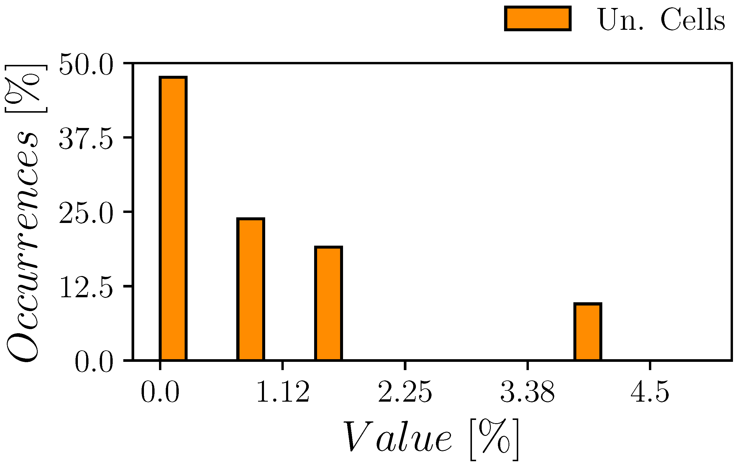
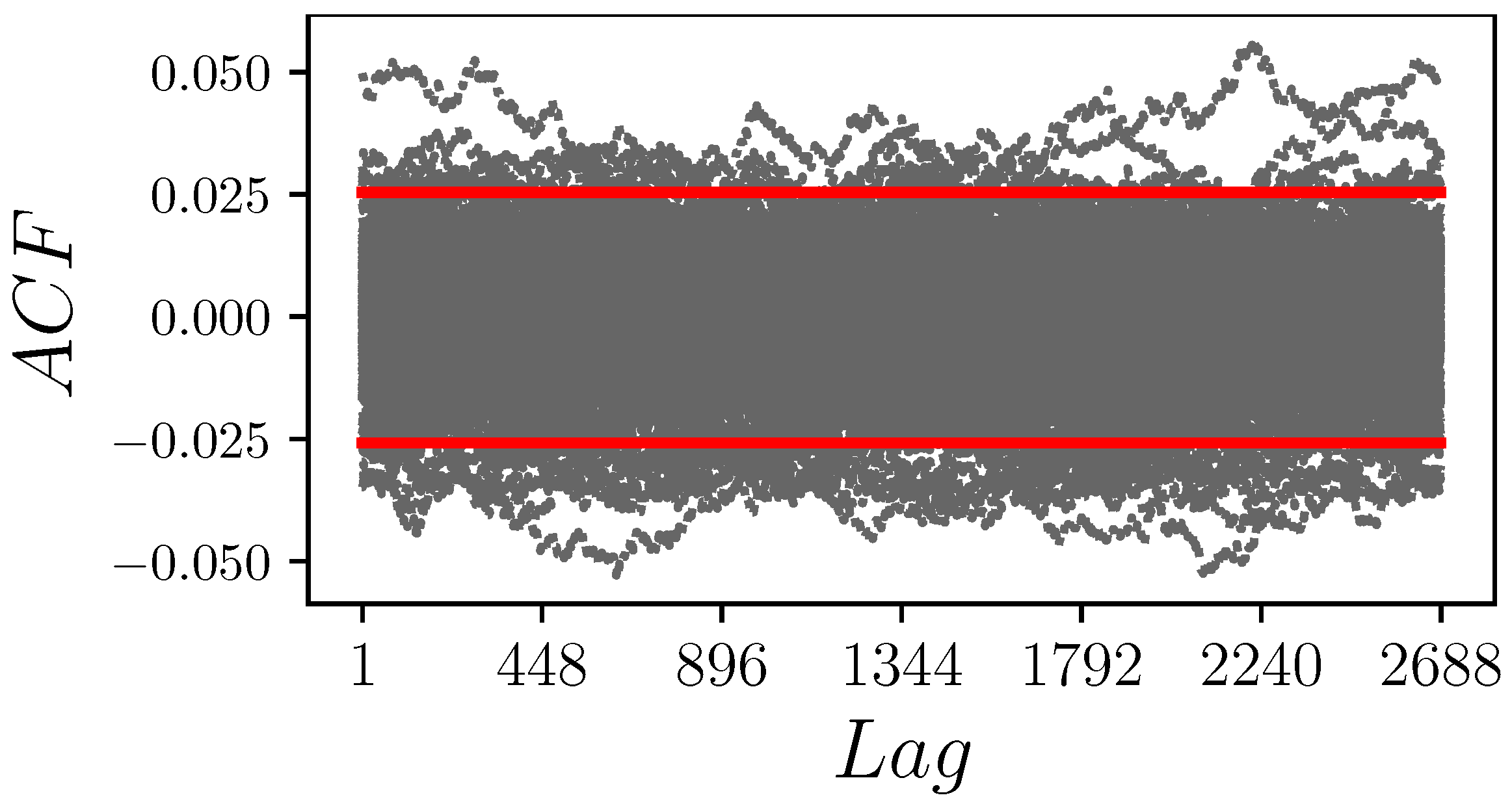
4.4. Randomness Validation

Since the sequences extracted from PUFs must satisfy strict requirements in terms of randomness, an ad-hoc test-suite has to be used to quantify the quality of the bitstream. For this purpose, we exploited NIST tests as in other works [3,23,29,30]. We considered a cumulative key of 2688 bits (128 bits extracted from each of the 21 measured samples) and for each test of Table 2 we evaluated the randomness by extracting the p-value. The p-value quantifies the bitstream performance with respect to a given test (e.g., the cumulative sum test) and if the p-value is greater than 0.01 (i.e., a 99% confidence level has been considered), then the test is successfully passed and the bitstream satisfies the test requirement. In Table 2, the p-value result is reported for each test which confirms that the bistream passed the statistical tests.

5. Figures of Merit and Performance Evaluation Metrics

In order to compare different architectures and implementations in terms of the tradeoff between H D i n t r a and H D i n t e r we used the following F O M H D :
F O M H D = 1 H D i n t r a · 0.5 H D i n t e r
According to the above definition, the greater the F O M H D , the better the achieved trade-off between H D i n t e r and H D i n t r a .
Moreover, since many solutions have to deal with strict requirements in terms of silicon Area on ASIC [3,25,28] or resource consumption on FPGA [1,4,29,30], we introduce the area-normalized F O M H D ^ , defined as:
F O M H D ^ = F O M H D A r e a b i t · A r e a m i n
where A r e a b i t denotes the Area/bit of the PUF bit cell and A r e a m i n is a normalization factor equal to the feature size of the technology squared, (E.g., for a 130 nm technology, the A r e a m i n 0.0169 µm 2 ).
Then, in order to evaluate bit-stream resiliency with respect to supply voltage ( V D D ) and temperature (T) fluctuations we define two BER normalization metrics as follows:
B E R ^ V = B E R w c V V D D m a x V D D m i n V D D t y p B E R ^ T = B E R w c T T m a x T m i n T t y p
where it has been denoted with B E R w c V ( T ) the worst case B E R associated with V D D (temperature) variations and with V D D m a x V D D m i n ( T m a x T m i n ) the V D D (T) range with respect to the typical value V D D t y p ( T t y p ) considered for the evaluation of B E R .
Analogously to B E R ^ V , T we can define the normalized metrics for the unstable bits (UB): U B ^ V , T defined as:
U B ^ V = U B w c V V D D m a x V D D m i n V D D t y p U B ^ T = U B w c T T m a x T m i n T t y p
where U B w c V ( T ) denoted the worst case U B associated with V D D (temperature) variations and V D D m a x V D D m i n ( T m a x T m i n ) represent the V D D (T) range with respect to the typical value V D D t y p ( T t y p ) considered for the evaluation of U B .
In addition, since it is important that both supply voltage and temperature resilience are addressed in a PUF design, we introduce two figures of merit, defined as follows:
F O M B E R = B E R t y p 2 + B E R V ^ 2 + B E R T ^ 2
F O M U B = U B t y p 2 + U B V ^ 2 + U B T ^ 2
which have the aim of quantifying B E R and U B performance in the different operating conditions, while considering also the typical values.

6. Comparison with the State-of-the-Art

The proposed IRCCM PUF has been compared with the literature, showing state of the art performances as reported in Table 3. In order to make a fair comparison, for nominal conditions, we used the mean value of the Bit Error Rate taken from measurements over 21 chip samples. In particular, the mean value of Unstable Cells reported in Table 3 also refers to measurements over 21 chip samples. As it can be observed, the proposed PUF outperforms all other works in terms of native unstable bits, both in the typical case and considering supply voltage and temperature variations, resulting in lower F O M B E R and F O M U B . These performances are due both to the well defined bias current, and to the higher output resistance of the IRCCM. It is worth noting that, if compared with previously proposed solutions based on cascode current mirrors in this work, we considered a wider supply voltage and temperature ranges for the redevaluation of performance metrics. The Energy per bit and the autocorrelation function performance result are both in line with those presented in the literature. For the entropy, the proposed PUF exhibits a value lower than just [31]. Finally, the H D i n t e r , i n t r a results are in line with the literature, as it can be observed by the F O M H D and also F O M ^ H D .

7. Conclusions

In this work, we have proposed a novel monostable PUF based on an IRCCM, which provides a well-defined bias current and a higher output resistance with respect to previous works [3,23]. The proposed PUF has been implemented on a 130 nm test-chip and measurements have been carried out considering a wide range of test-chip samples and environmental conditions. Measurement results have shown that the proposed IRCCM PUF exhibit an H D i n t r a 0.491 % and a native bit instability of 0.586 % , which is the lowest value compared to the designs in Table 3. In the ±10% V D D range, the worst case H D i n t r a is lower than 1.5 % whereas in the very extended supply voltage range (−25% to +50% V D D ) it is about 2.34%. Furthermore, it has been found that the proposed architecture can show a uniqueness of 50.12, measured over 21 test-chip samples.

Author Contributions

Conceptualization, R.D.S. and G.S.; methodology, R.D.S. and G.S.; software, R.D.S., D.B. and G.S.; validation, R.D.S. and G.S.; formal analysis, R.D.S.; investigation, R.D.S.; resources, G.S.; data curation, R.D.S.; writing—original draft preparation, R.D.S.; writing—review and editing, G.S. and F.C.; visualization, G.S. and F.C.; supervision, G.S.; project administration, G.S.; funding acquisition, G.S. All authors have read and agreed to the published version of the manuscript.

Funding

This research received no external funding.

Informed Consent Statement

Not applicable.

Data Availability Statement

Not applicable.

Conflicts of Interest

The authors declare no conflict of interest.

References

  1. Della Sala, R.; Bellizia, D.; Scotti, G. A Lightweight FPGA Compatible Weak-PUF Primitive Based on XOR Gates. IEEE Trans. Circuits Syst. II 2022, 69, 2972–2976. [Google Scholar] [CrossRef]
  2. Gassend, B.; Clarke, D.; van Dijk, M.; Devadas, S. Silicon physical random functions. In CCS ’02: Proceedings of the 9th ACM Conference on Computer and Communications Security; Association for Computing Machinery: New York, NY, USA, 2002; pp. 148–160. [Google Scholar] [CrossRef]
  3. Alvarez, A.B.; Zhao, W.; Alioto, M. Static Physically Unclonable Functions for Secure Chip Identification with 1.9–5.8% Native Bit Instability at 0.6–1 V and 15 fJ/bit in 65 nm. IEEE J. Solid-State Circuits 2016, 51, 763–775. [Google Scholar]
  4. Della Sala, R.; Bellizia, D.; Scotti, G. A Novel Ultra-Compact FPGA PUF: The DD-PUF. Cryptography 2021, 5, 23. [Google Scholar] [CrossRef]
  5. Sala, R.D.; Scotti, G. The DD-Cell: A Double Side Entropic Source exploitable as PUF and TRNG. In Proceedings of the 2022 17th Conference on Ph.D Research in Microelectronics and Electronics (PRIME), Villasimius, Italy, 12–15 June 2022; pp. 353–356. [Google Scholar]
  6. Liu, C.Q.; Cao, Y.; Chang, C.H. ACRO-PUF: A Low-power, Reliable and Aging-Resilient Current Starved Inverter-Based Ring Oscillator Physical Unclonable Function. IEEE Trans. Circ. Syst. I 2017, 64, 3138–3149. [Google Scholar] [CrossRef]
  7. Cao, Y.; Zhang, L.; Chang, C.H.; Chen, S. A Low-Power Hybrid RO PUF with Improved Thermal Stability for Lightweight Applications. IEEE Trans. Comput. Aided Des. Integr. Circuits Syst. 2015, 34, 1143–1147. [Google Scholar]
  8. Rahman, M.T.; Forte, D.; Fahrny, J.; Tehranipoor, M. ARO-PUF: An aging-resistant ring oscillator PUF design. In Proceedings of the In 2014 Design, Automation & Test in Europe Conference & Exhibition (DATE), Dresden, Germany, 24–28 March 2014; pp. 24–28. [Google Scholar]
  9. Lee, J.W.; Lim, D.; Gassend, B.; Suh, G.E.; van Dijk, M.; Devadas, S. A technique to build a secret key in integrated circuits for identification and authentication applications. In Proceedings of the 2004 Symposium on VLSI Circuits. Digest of Technical Papers (IEEE Cat. No.04CH37525), Honolulu, HI, USA, 17–19 June 2004; pp. 176–179. [Google Scholar] [CrossRef]
  10. Sahoo, D.P.; Mukhopadhyay, D.; Chakraborty, R.S.; Nguyen, P.H. A Multiplexer-Based Arbiter PUF Composition with Enhanced Reliability and Security. IEEE Trans. Comput. 2017, 67, 403–417. [Google Scholar] [CrossRef]
  11. Zhou, C.; Parhi, K.K.; Kim, C.H. Secure and Reliable XOR Arbiter PUF Design: An Experimental Study based on 1 Trillion Challenge Response Pair Measurements. In DAC ’17: Proceedings of the 54th Annual Design Automation Conference 2017; Association for Computing Machinery: New York, NY, USA, 2017; pp. 1–6. [Google Scholar] [CrossRef]
  12. Majzoobi, M.; Koushanfar, F.; Devadas, S. FPGA PUF using programmable delay lines. In Proceedings of the 2010 IEEE International Workshop on Information Forensics and Security, Seattle, WA, USA, 12–15 December 2010; pp. 12–15. [Google Scholar]
  13. Machida, T.; Yamamoto, D.; Iwamoto, M.; Sakiyama, K. A new mode of operation for arbiter PUF to improve uniqueness on FPGA. In Proceedings of the 2014 Federated Conference on Computer Science and Information Systems, Warsaw, Poland, 7–10 September 2014; pp. 7–10. [Google Scholar] [CrossRef]
  14. Fruhashi, K.; Shiozaki, M.; Fukushima, A.; Murayama, T.; Fujino, T. The arbiter-PUF with high uniqueness utilizing novel arbiter circuit with Delay-Time Measurement. In Proceedings of the 2011 IEEE International Symposium of Circuits and Systems (ISCAS), Rio de Janeiro, Brazil, 15–18 May 2011; pp. 15–18. [Google Scholar] [CrossRef]
  15. Paral, Z.; Devadas, S. Reliable and efficient PUF-based key generation using pattern matching. In Proceedings of the 2011 IEEE International Symposium on Hardware-Oriented Security and Trust, San Diego, CA, USA, 5–6 June 2011; pp. 5–6. [Google Scholar] [CrossRef] [Green Version]
  16. Serrano, R.; Duran, C.; Sarmiento, M.; Dang, T.K.; Hoang, T.T.; Pham, C.K. A Unified PUF and Crypto Core Exploiting the Metastability in Latches. Future Internet 2022, 14, 298. [Google Scholar] [CrossRef]
  17. Bossuet, L.; Ngo, X.T.; Cherif, Z.; Fischer, V. A PUF Based on a Transient Effect Ring Oscillator and Insensitive to Locking Phenomenon. IEEE Trans. Emerging Top. Comput. 2013, 2, 30–36. [Google Scholar] [CrossRef]
  18. Habib, B.; Kaps, J.P.; Gaj, K. Efficient SR-Latch PUF. In Applied Reconfigurable Computing; Springer: Cham, Switzerland, 2015; pp. 205–216. [Google Scholar] [CrossRef]
  19. Yamamoto, D.; Sakiyama, K.; Iwamoto, M.; Ohta, K.; Ochiai, T.; Takenaka, M.; Itoh, K. Uniqueness Enhancement of PUF Responses Based on the Locations of Random Outputting RS Latches. In Cryptographic Hardware and Embedded Systems—CHES 2011; Springer: Berlin, Germany, 2011; pp. 390–406. [Google Scholar] [CrossRef]
  20. Yang, K.; Dong, Q.; Blaauw, D.; Sylvester, D. 14.2 A physically unclonable function with BER <10-8 for robust chip authentication using oscillator collapse in 40nm CMOS. In Proceedings of the 2015 IEEE International Solid-State Circuits Conference-(ISSCC) Digest of Technical Papers, San Francisco, CA, USA, 22–26 February 2015; pp. 1–3. [Google Scholar]
  21. Mathew, S.K.; Satpathy, S.K.; Anders, M.A.; Kaul, H.; Hsu, S.K.; Agarwal, A.; Chen, G.K.; Parker, R.J.; Krishnamurthy, R.K.; De, V. 16.2 A 0.19pJ/b PVT-variation-tolerant hybrid physically unclonable function circuit for 100% stable secure key generation in 22nm CMOS. In Proceedings of the 2014 IEEE International Solid-State Circuits Conference Digest of Technical Papers (ISSCC), San Francisco, CA, USA, 9–13 February 2014; pp. 278–279. [Google Scholar]
  22. Shifman, Y.; Miller, A.; Keren, O.; Weizmann, Y.; Shor, J. A Method to Improve Reliability in a 65-nm SRAM PUF Array. IEEE Solid-State Circuits Lett. 2018, 1, 138–141. [Google Scholar] [CrossRef]
  23. Taneja, S.; Alvarez, A.B.; Alioto, M. Fully Synthesizable PUF Featuring Hysteresis and Temperature Compensation for 3.2% Native BER and 1.02 fJ/b in 40 nm. IEEE J. Solid-State Circuits 2018, 53, 2828–2839. [Google Scholar] [CrossRef]
  24. Vatalaro, M.; De Rose, R.; Lanuzza, M.; Crupi, F. Static CMOS Physically Unclonable Function Based on 4T Voltage Divider with 0.6%–1.5% Bit Instability at 0.4–1.8 V Operation in 180 nm. IEEE J. Solid-State Circuits 2022, 57, 2509–2520. [Google Scholar] [CrossRef]
  25. Zhao, Q.; Wu, Y.; Zhao, X.; Cao, Y.; Chang, C.H. A 1036-F2/Bit High Reliability Temperature Compensated Cross-Coupled Comparator-Based PUF. IEEE Trans. Very Large Scale Integr. VLSI Syst. 2020, 28, 1449–1460. [Google Scholar] [CrossRef]
  26. Asghari, M.; Guzman, M.; Maghari, N. Cross-Coupled Impedance-Based Physically Unclonable Function (PUF) with 1.06% Native Instability. IEEE Solid-State Circuits Lett. 2020, 3, 282–285. [Google Scholar] [CrossRef]
  27. Zhao, X.; Gan, P.; Zhao, Q.; Liang, D.; Cao, Y.; Pan, X.; Bermak, A. A 124 fJ/Bit Cascode Current Mirror Array Based PUF with 1.50% Native Unstable Bit Ratio. IEEE Trans. Circ. Syst. I 2019, 66, 3494–3503. [Google Scholar] [CrossRef]
  28. Yang, K.; Dong, Q.; Blaauw, D.; Sylvester, D. 8.3 A 553F2 2-transistor amplifier-based Physically Unclonable Function (PUF) with 1.67% native instability. In Proceedings of the 2017 IEEE International Solid-State Circuits Conference (ISSCC), San Francisco, CA, USA, 5–9 February 2017; pp. 146–147. [Google Scholar]
  29. Della Sala, R.; Bellizia, D.; Scotti, G. A Novel Ultra-Compact FPGA-Compatible TRNG Architecture Exploiting Latched Ring Oscillators. IEEE Trans. Circuits Syst. II 2021, 69, 1672–1676. [Google Scholar] [CrossRef]
  30. Della Sala, R.; Bellizia, D.; Scotti, G. High-Throughput FPGA-Compatible TRNG Architecture Exploiting Multistimuli Metastable Cells. IEEE Trans. Circ. Syst. I 2022, 69, 4886–4897. [Google Scholar] [CrossRef]
  31. Satpathy, S.; Mathew, S.K.; Suresh, V.; Anders, M.A.; Kaul, H.; Agarwal, A.; Hsu, S.K.; Chen, G.; Krishnamurthy, R.K.; De, V.K. A 4-fJ/b Delay-Hardened Physically Unclonable Function Circuit with Selective Bit Destabilization in 14-nm Trigate CMOS. IEEE J. Solid-State Circuits 2017, 52, 940–949. [Google Scholar] [CrossRef]
Figure 1. Proposed PUF Architecture.
Electronics 12 00755 g001
Figure 2. Test-chip picture (a), layout of the array of 128 PUF bitcells (b) and the single IRCCM PUF cell (c).
Electronics 12 00755 g002
Figure 3. Histogram of Unstable Cells over the 21 chip samples.
Electronics 12 00755 g003
Figure 4. Histogram of the Bias for the 128-bits PUF key over the 21 chip samples.
Electronics 12 00755 g004
Figure 5. Graphical representation of 128-bits PUF keys over the 21 chip samples.
Electronics 12 00755 g005
Figure 6. Histogram of the Reliability in terms of H D i n t r a measured over 21 chip samples.
Electronics 12 00755 g006
Figure 7. Histogram of the Uniqueness in terms of H D i n t e r measured over 21 chip samples.
Electronics 12 00755 g007
Figure 8. Autocorrelation Function of the measured PUF outputs: red lines denote the boundary of the 95% confidence level.
Electronics 12 00755 g008
Figure 9. Unstable Cells and BER in percentage under voltage variations over 5 chips, average trend highlighted in green and red colors.
Electronics 12 00755 g009
Figure 10. Unstable Cells and BER in percentage under temperature variations over 5 chips, average trend highlighted in blue color.
Electronics 12 00755 g010
Table 1. Transistors’ sizing.
M n b 1 M n b 2 M p b 1 M p b 2 M n g b 1 M n g b 2 M n o 1 M n o 2
W [nm]0.7353·0.6254·0.4204· 1.0650.7350.6200.7303·0.62
M n m 1 M n m 2 M p m 1 M p m 2 M p g b 1 M p g b 2 M p o 1 M p o 2
W [nm]0.7303·0.6204·0.4204· 1.0654·0.4204·1.0604· 0.4204· 1.060
Table 2. NIST Tests.
NIST TestStream Lengthp-ValueResult
Frequency26880.1897
Frequency block26880.4081
Runs26880.2948
Longest Run26880.6436
DTFT26880.2724
Non Overlapping26880.5445
Serial2688 (m = 9)0.8631
Approximate Entropy2688 (m = 6)0.7702
Cumulative Sum26880.0481
Table 3. Comparison Table.
This Work[21][27][31][28][23][3]
Technology [nm]1302265141804065
Area/bit [ µm 2 ]72.034.6612.91158.9413.2261.5886.4
F @130nm
Area/bit normalized4262.139628.107649404.73782.253643.795114.79
Typ V D D [V]0.80.91.200.650.80.91
V D D range * [V][0.6–1.2][0.7–0.9][0.95, 1.30][0.55–0.75][0.8–1.8][0.6–1.2][0.6–1]
T Range [°C][0, 75][25, 50][−40, 120]-[−40, 120][−40, 125][25, 85]
Energy/bit (fj/bit)5.361312441.711.0215
Un. Bits [ % ] 0.5865 τ 1.5026.81.732.552.34
in Typ. Condition
number of evaluation5005k500-2000500400
# Bits128256112810243000256
Entropy0.999840.997-0.99993-0.99720.9967
ACF @ 95% c.l. 0.0250.0880.019-0.0170.0070.036
μ H D i n t r a [ % ] 0.4910.97 τ -3.40.180.490.861
μ H D i n t e r [ % ] 50.1249.0049.9448.6049.8049.0750.14
F O M H D [ % ] 16.971.0318.320.2127.782.198.30
F O M H D ^ [ % ] 3.98 ×   10 3 0.10 ×   10 3 2.40 ×   10 2 2.23 ×   10 5 3.55 ×   10 5 6.02 ×   10 4 1.62 ×   10 3
B E R t y p [ % ] 0.490.97 τ 16.971.460.182.38-
B E R ^ V [ % ] 3.12-5.629.753.364.34-
B E R ^ T [ % ] 0.35-0.460.950.620.94-
F O M B E R [ % ] 3.18-5.649.903.425.04-
U B t y p [ % ] 0.8565 τ 1.50-1.703.481.88
U B ^ V [ % ] 2.08---3.489.008.83
U B ^ T [ % ] 1.25---4.2015.7510.75
F O M U B [ % ] 2.57---5.7118.4714.03
* Supply Voltage Range; Area of the PUF cell normalized to the minimum feature size of a 130 nm technology; Confidence Level; τ Refers to measurements carried out after TMV, Burn-in and Dark bits soft mask.
Disclaimer/Publisher’s Note: The statements, opinions and data contained in all publications are solely those of the individual author(s) and contributor(s) and not of MDPI and/or the editor(s). MDPI and/or the editor(s) disclaim responsibility for any injury to people or property resulting from any ideas, methods, instructions or products referred to in the content.

