Article

A Compact Current-Transfer Model in Resonant-Tunneling Structures with Consideration of Interelectronic Interaction

Research Institute of Radio Electronics and Laser Technology, Bauman Moscow State Technical University, 105005 Moscow, Russia
*
Authors to whom correspondence should be addressed.
Electronics 2023, 12(3), 519; https://doi.org/10.3390/electronics12030519
Submission received: 29 November 2022 / Revised: 30 December 2022 / Accepted: 13 January 2023 / Published: 19 January 2023
(This article belongs to the Section Semiconductor Devices)

Abstract

:
A compact analytical model of current transfer was developed to estimate the characteristics of heterostructured devices. The absence of empirical correction factors and the explicit accounting of the interelectronic interaction differentiates it from previous similar models. The model obtains an estimates of the electron density in the quantum well of the heterostructural channel and applies a self-consistent correction for resonance levels. It also provides accuracy in the positive differential resistance region of the I–V characteristics in the AlGaAs structures, with an average relative error not exceeding 2%. The time complexity of the calculations of the I–V characteristics using this model is several orders of magnitude less than that of calculations using ab initio models. Its high accuracy and low temporal complexity of calculations of I–V characteristics allow this model to be integrated in systems for the design and calculation of reliability indicators for devices, including terahertz devices.

1. Introduction

Radio waves in the terahertz (THz) range lack ionizing effects, can penetrate optically opaque objects, are capable of forming a narrow radio beam and have a high information capacity. For these reasons, they are able to operate in a complex electromagnetic environment and are widely used for the creation of high-speed radio communication lines, high-precision radars, high-resolution imaging devices and remote chemical identification devices for security systems. Terahertz waves are widely used in astrophysical research to study background cosmic radiation and the radiation specters of stars, galaxies and other cosmic objects.
Terahertz radiation is relatively safe for humans. It is increasingly used in tomography and other medical research, in particular as an effective complement to X-ray diagnosis of living tissue pathologies. Methods of treatment and surgical intervention using terahertz radio waves are also notably found in oxidation therapy, aerotherapy, inhalation therapy and in oncology treatment for the thermal destruction of tissues.
In addition, a transition to the THz range can significantly reduce equipment size and resolve the electromagnetic compatibility problems of radio systems located in close proximity to each other, their noise immunity and the stealth of information transfer, as well as reduce power consumption through the use of antennae with a narrow radiation pattern and a high amplification factor.
Key elements of receiving and transmitting devices in such systems are devices that perform frequency conversions of radio signals (mixers, multipliers, etc.), which are built, as a rule, on GaAs Schottky barrier diodes (SBD) as nonlinear elements (NE). The characteristics of nonlinear conversions (level of useful signal, conversion loss, levels of parasitic harmonics and intermodulation frequencies, dynamic range of processed signals, etc.) that determine the quality of a system performance, depend on the shape of the NE current–voltage characteristics (or I–V curve). For Schottky barrier diodes, this is exponential and cannot be changed, which limits the acceptable solutions in the design and manufacture of such devices. To eliminate parasitic harmonics and undesirable intermodulation frequencies from the output signal spectrum, filtering is used, which leads to more complex design, reduced reliability and increased mass–size characteristics.
These drawbacks can be overcome by using RTDs based on multilayer nanoheterostructures as NE devices for the frequency conversion of radio signals. The use of RTDs for such devices has the following advantages:
  • In the design of the RTD, the shape of the I–V curve can be varied by selecting the parameters of the resonant-tunneling heterostructure (RTHS), which, in turn, opens up the possibility of purposeful change in the electrical characteristics of converters that are based on it [1,2,3,4,5,6,7,8].
  • The range of possible frequency conversions using RTD is wide: generations of radio signals on the falling segment of the I–V curve, mixing, frequency multiplication of radio signals, amplitude detection and rectification on the rising segment of the I–V curve [9,10,11,12,13,14].
  • The maximum operating frequency of the RTD extends up to units of THz, which makes RTD a promising element of radiophotonic and optoelectronic devices [15,16,17].
  • Specific symmetry with respect to the origin I–V curve waveform (anti-symmetric) allows the circuitry realization of some types of frequency converters to be simplified. In particular, in the construction of THz range frequency mixers, a scheme with subharmonic pumping is used, which enables the frequency of the heterodyne to be reduced and the design and technological implementation of the heterodyne circuit to be simplified. To suppress the odd harmonics of the heterodyne, the NE I–V curve must be anti-symmetrical, for which two counter-connected SBDs are used. When using RTDs as the NE in such circuits, one diode is sufficient. This increases the reliability of the converter and avoids the requirement to select two SBDs with identical parameters.
  • An RTD functioning in the typical range of external influences for technical applications and its production can be achieved using proven technologies in semiconductor electronics.
To design a converter based on RTD with the required parameters, it is necessary to carefully select the optimal I–V curve and corresponding diode design. The I–V curve calculation method should, on the one hand, provide a good qualitative and quantitative agreement of experimental calculations, and on the other hand, have low requirements for computing resources for multiple I–V curve calculations in an acceptable time.
From this point of view, the prediction of I–V characteristics is currently an unsolved problem. Existing models [18,19,20] do not enable the I–V curvature to be predicted as well as the peak current and voltage. In addition, there is a problem with the computational efficiency of current-transfer models in RTDs: calculation of even one I–V characteristic with satisfactory accuracy has an unacceptably high algorithmic complexity for solving inverse problems (e.g., self-consistent multivalley I–V curve calculation using model [20] requires about 2 h of CPU time on an Intel Core i5 processor).
To understand the sources of these problems, let us consider the modeling methods for electronic devices, which can be divided into two groups: empirical, i.e., using the dependencies obtained from the experiment, and theoretical, the calculation of characteristics from first principles [19].
Semiempirical models, in which experimental data are used to simplify the equations of theoretical models, are a borderline variant [21,22]. The development of models using experimental data usually implies the application of regression analysis methods, including the use of artificial neural networks [23,24]. This presents a problem in relation to staging and conducting the experiment, too many data are required (which in most cases is simply not available at the design stage of the RTD-based devices) because of the need to establish the dependencies of a large number of operating parameters on an equally large number of factors.
Thus, the use of a theoretical approach is believed to be more promising. Obviously, when designing, the most effective approaches should be built on the minimum number of “correction” (and in fact, fitting) empirical coefficients (ideally with none) and have both qualitative and quantitative validity. If these conditions can be met, validation of the current-transfer model using experimental data can be carried out with high confidence levels and small error values.
However, this presents a further problem: to calculate the RTD characteristics with satisfactory accuracy, a numerical solution for the system of differential and integral equations of the current-transfer model is required, which implies the use of significant computing resources. This makes it difficult to use ab initio models in applications that require multiple calculations of RTD characteristics, e.g., in the design of integrated circuits or in predicting their reliability indicators [25,26,27].
The solution is to use "compact" models, which have obvious advantages in terms of the time complexity of algorithms and physical "transparency" (the possibility of analysis and physical interpretation of model parameters obtained at each stage of the calculation of the I–V curve, in particular, the concentration of charge carriers). However, it is important to avoid an unacceptable decrease in accuracy for engineering calculations in the area of positive differential conductivity.
To date, there are a number of compact models of current transfer in heterostructured devices [28,29,30,31,32,33,34,35], which do not have the drawbacks of ab initio models. In broad terms, these models include the processes of elastic and inelastic dissipation. However, in these models, the accounting of the interelectronic interaction, which has a significant influence on current-transfer processes, is carried out in a rather crude way.
In theoretical models of current transfer, the interelectronic interaction is taken into account using the self-consistent field method, which introduces a correction to the total energy of the electrons, whereas, in compact models, a correction to the resonant energy levels is introduced to take account of the interelectronic interaction.
At present, there are no strict methods for calculating the correction to the resonance levels. It is usually assumed to be equal to some constant value (not depending on the voltage) and is considered as a model parameter to be selected during the validation of the calculation results. Consequently, this approach makes it impossible to solve the inverse design problem. Thus, the aim of our work was to build an effective (“easy” in computational complexity and physically interpretable) model of current transfer in resonant-tunnel structures with an adequate “a priori” estimation of the position of resonant levels.

2. Modeling Methodology

2.1. Initial Model

In order to verify the developed compact model, it is appropriate to use one of the existing and well-developed current-transfer models based on integral-differential equations with a high validation level, e.g., the combined model [20]. This model is based on the formalism of envelope wave functions, which are the Schrödinger equation solutions for an open system, and the account of the spatial charge distribution in heterostructures is performed using the self-consistent field method by entering the averaged electron interaction potential and the self-consistent potential into the Hamiltonian [36,37,38,39,40].
The basic idea behind the development of a compact model is that a system of integral and differential equations of the verification basis can be transformed into algebraic and transcendental equations via linearization and decomposition.
These methods are based on splitting systems of coupled equations into several simpler independent equations. Decomposition greatly simplifies the qualitative investigation and interpretation of important physical properties described by coupled equations, allowing their waves and dissipative properties to be studied effectively.
In addition, in some cases decomposition makes it possible to obtain exact analytical solutions to the corresponding boundary and initial boundary value problems, and greatly simplifies the application of numerical methods. These advantages support the goal of developing a compact model of current transfer in resonant-tunneling structures (RTS), taking into account the interelectronic interaction.
The construction of an effective model was based on three assumptions:
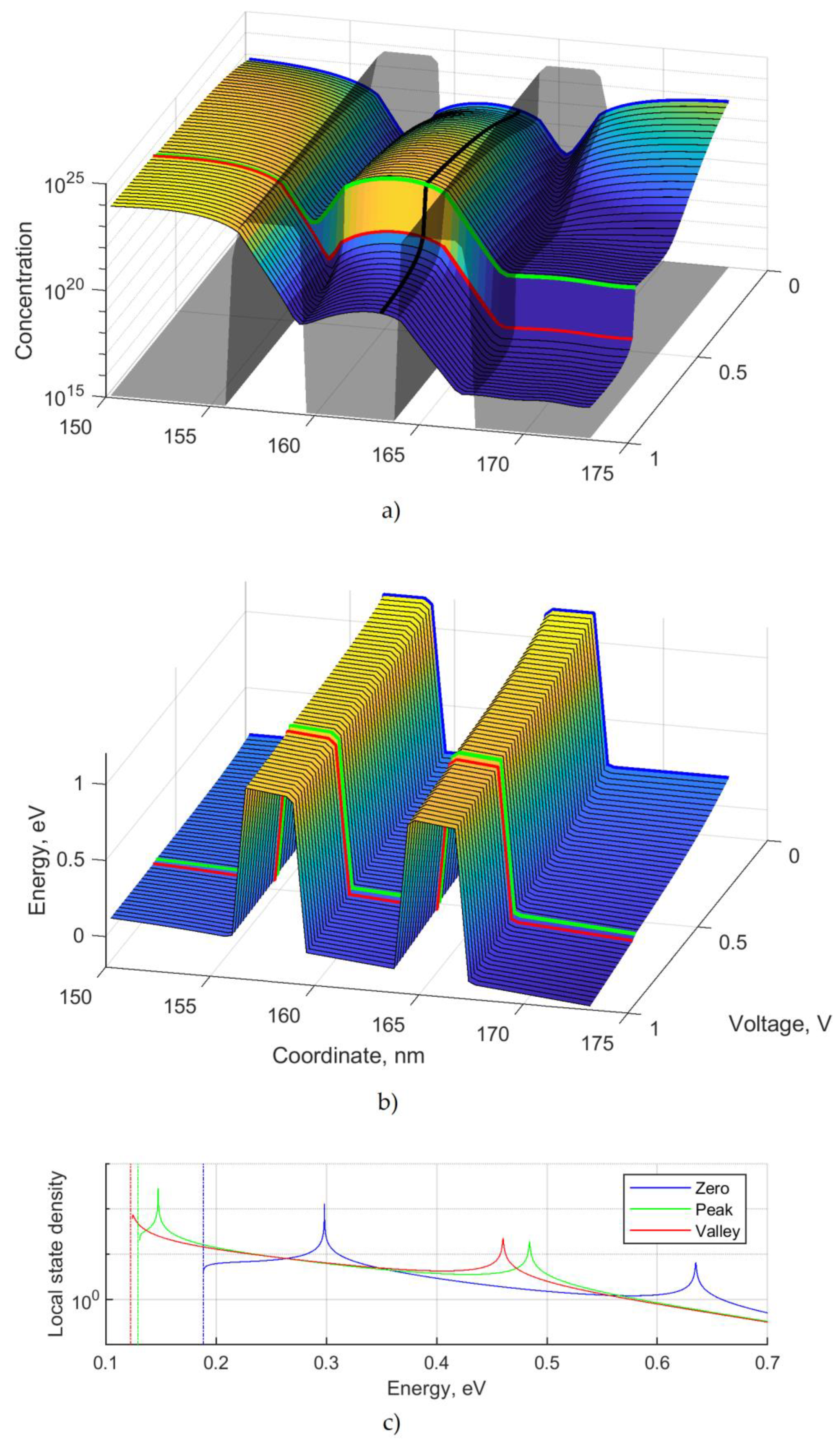
  • The current density and concentration of electrons in the quantum well is caused by energy-charged electrons in the vicinity of the lowest resonance level, formed in the conduction zone of the RTS quantum well.
  • The width of the resonant levels is negligibly small compared with thermal energy.
  • The tunnel transparency coefficient and local density of states as a function of energy in the vicinity of resonant levels can be approximated by a function proportional to the Lorentz distribution function.

2.2. Current Density and Resonant Levels

Figure 1 shows the I–V curve of the resonant-tunneling structures (RTS) and the tunnel transparency coefficient.
It can be seen from the graphs that the current density drop coincides with the jumping of the lowest resonant level into the forbidden band. It is therefore worth considering the dependence of current density on the position of the lowest resonant level. According to the Tsu–Esaki formula, the current through the RTD active region is described by the following formula [32,36]:
J ( V ) = J 0 E c T ( E , V ) D ( E , V ) d E ,
where J 0 = 2 2 m * q e k Б T ( 2 π ) 2 ħ 3 is a ratio factor, E is a transverse component of the total electron energy, V is an external voltage, E c is the position of the bottom of the conduction zone at the source, T ( E , V ) is the tunnel transparency coefficient and D ( E , V ) is the supply function.
The supply function is defined as:
D ( E , V ) = { ln 1 + e E F E k T 1 + e E F q e V E k T E E c 0 E < E c ,
where E F is Fermi level, q e is the elementary charge, k T is thermal energy (Boltzmann constant multiplied by absolute temperature) and m * is the effective mass of electrons in reservoirs.
In the Tsu–Esaki formula, the integration is performed along the energy spectrum, starting from the bottom of the conduction zone. According to the first assumption, current through the channel is caused by electrons at the lower resonant level (Figure 1); thus, the integration should be performed only in the vicinity of the lower resonant level, that is in Formula (1), integration limits are changing:
J ( V ) = J 0 ε Γ ε + Γ T ( E , V ) D ( E , V ) d E ,
where ε = ε ( V ) is the energy of the lowest resonance level in the permitted band and Γ is the half-width of that level.
According to the second assumption, the width of the resonant levels is sufficiently small. Therefore, the supply function can be considered constant in the integration section. This allows us to take it beyond the integral sign:
J ( V ) = J 0 D ( E , V ) ε Γ ε + Γ T ( E , V ) d E .
According to the third assumption, in the vicinity of the lowest resonance level, the tunnel transparency coefficient is approximated by the Lorentz curve.
T ( E , V ) = Γ 2 ( E ε ) 2 + Γ 2 ,
Substituting this approximation into the Tsu–Esaki Formula (1), we obtain:
J ( V ) = π 2 J 0 Γ D ( ε , V ) .
Thus, in order to calculate the current density as a function of voltage, it is necessary to know the voltage dependence of the resonant level position ε ( V ) , which can be written in the form:
ε ( V ) = ε 0 + ϕ ( V ) ,
where ε 0 is the position of the resonant level at zero voltage without taking into account self-consistency, and ϕ ( V ) is the correction to the resonance levels because of external voltage and interelectronic interactions.
The position of the resonance level ε 0 and its half-width Γ are calculated based on the barrier thickness and pit width [36]. Without taking into account the Coulomb interaction of electrons, the correction ϕ ( V ) in the center of a symmetric RTS equals q e V / 2 . If self-consistency is taken into account, the correction to the resonant levels can be calculated from the Poisson equation:
d d z σ ( z ) d d z φ ( z , V ) = q e ( n ( z , V ) N D ( z ) ) ,
where σ ( z ) is the permittivity, N D ( z ) is the concentration of donor impurities, z is the coordinate and n ( z , V ) is the concentration of electrons.
The solution to Equation (8) is the following function:
φ ( z , V ) = q e 0 z 1 σ ( z ) ( 0 z ( n ( z , V ) N D ( z ) ) d z + C 1 ) d z + C 2 ,
where the constants C 1 and C 2 are obtained from the boundary conditions.
Boundary conditions for Equation (8) are the equality of the potentials to zeroat the source and applied voltage at the drain. The correction to the resonant levels equals ϕ ( V ) = q e φ ( z c , V ) , where z c is the center of the quantum well. Thus, to calculate the self-consistent correction, it is necessary to determine the concentration of electrons.

2.3. Electron Concentration

Figure 2 shows the electron concentration and self-consistent potential calculated using the original model. It can be seen that the departure of the lowest resonance level leads to a drop in the concentration and self-consistent potential. It also shows that the concentration of electrons in the barriers can be neglected. Next, it is necessary to consider the concentration of electrons in the quantum well, spacers and reservoirs.
The concentration of electrons in the channel is the sum of the concentrations of electrons entering the channel from the source and the drain:
n ( z , V ) = n s + n d ,
where n s is the concentration of the source electrons and n d is the concentration of the drain electrons.
The concentration of source electrons in the channel is described by the following Formula [36]:
n s = E s | ψ ( z , E ) | 2 g s ( E ) d E ,
where ψ ( E , z ) is the wave function z and g s ( E ) is the energy distribution function of the source electrons at point z.
Function g s ( E ) is defined as:
g s ( E ) = C n ln ( 1 + e E + E F + U L ( R ) k T ) E U l ( r ) , C n = 2 m * 3 2 k T ( 2 π ) 2 ħ 3 .
where U L ( R ) is the potential energy of an electron on the left (right) boundary of the simulated area, U l ( r ) is the potential energy of an electron at the channel-source (drain) boundary.
To determine the concentration of source electrons in the quantum well, transformations similar to those applied to the Tsu–Esaki Formula (1) are applied to Equation (11), in order to obtain the formula for the current density (6). According to the first assumption, we replace the integration limits in Formula (11):
n s ( z ) ε Γ ε + Γ | ψ ( z , E ) | 2 g s ( E ) d E .
Applying the second assumption, the function g s ( E ) can be considered constant within the integration, which allows us to take it beyond the integral sign:
n s ( z ) g s ( E ) ε Γ ε + Γ | ψ ( z , E ) | 2 d E .
Thus, to obtain an analytical expression for the concentration of electrons in the quantum well, it is necessary to introduce an approximation of the wave function ψ ( z , E ) in the well. In this region, electron waves repeatedly reflect from barriers and form a standing wave, which is described by the following formula:
ψ ( z , E ) = A ( E ) cos ( k w ( z z c ) ) .
The parameters k w and z c determine the positions of concentration maxima and minima. Ignoring the displacement of the concentration maximum due to the applied electric field, we can approximately assume that z c is the coordinate of the center of the quantum well. The parameter k w can be estimated from the approximation that, at the depth of the barriers, the concentration of electrons tunneling out of the well is zero:
k w = π / ( a + b ) ,
where a is the quantum well thickness and b is the barrier thickness.
What remains unknown is the amplitude A ( E ) , which can be estimated using the transfer matrices method, by relating it to the amplitude of the passed wave. According to the third assumption, the square of the amplitude of the passed wave in the resonance level region is approximated by the following formula:
| t | 2 = | ψ ( L , E ) | 2 = Γ 2 ( E ε ) 2 + Γ .
In order to connect the amplitude of the passed wave to the amplitude of the wave function in the quantum well, it is necessary to determine the type of wave function in the drain barrier. For simplicity, the origin of coordinates is taken to be at the right-hand barrier boundary of the well. Then, ignoring the intra-barrier reflection, the wave function in the barrier has the form:
ψ b = A d e K d ( z , E ) ,
where K d ( z , E ) = 0 z k d ( x , E ) d x = 1 ħ 0 z 2 m d * ( U d ( x ) E ) d x , U d ( z ) is the potential electron energy in the drain barrier, m d * is the effective mass in the stock barrier and A d = t e K d ( b , E ) sec ( k w z c ) .
Thus, if the square of the modulus of the electron wave function in the quantum well in the vicinity of the resonance level is:
| ψ ( z , E ) | 2 = cos 2 ( k w ( z z c ) ) cos 2 ( k w z c ) Γ 2 e 2 K d ( b , E ) ( E ε ) 2 + Γ 2 ,
then the concentration of electrons equals:
n s ( z ) = g s ( ε ) cos 2 ( k w ( z z c ) ) cos 2 ( k w z c ) ε Γ ε + Γ Γ 2 e 2 K d ( b , E ) ( E ε ) 2 + Γ 2 d E .
The value e 2 K d ( b , E ) can be assumed constant within the limits of integration and therefore, can be carried beyond the integral sign. Next, the concentration of source electrons in the quantum well is approximated by the following formula:
n s ( z ) = π 2 Γ e 2 K d ( b , E ) g s ( ε ) cos 2 ( k w ( z z c ) ) cos 2 ( k w z c ) .
The formula for the concentration of electrons from the drain can be obtained in a similar way. Note that the position and width of the resonant level remain the same, the Fermi level decreases by q e V and the potential energy of the electron at the source-channel interface E s changes to the potential energy of the electron at the drain-channel interface E d , and E s < E d :
n d ( z ) = π 2 Γ e 2 K s ( b , E ) g d ( ε ) cos 2 ( k w ( z z c ) ) cos 2 ( k w z c ) ,
where K s ( b , E ) is defined for the source barrier in the same way as the function K d ( b , E ) is defined for the drain barrier.

2.4. Self-Consistent Potential

Thus, the formula for the concentration of electrons in the quantum well is obtained. Taking into account that the concentration of donor impurities in the barriers and the well is zero and that in the spacers and reservoirs the charges of electrons and donor impurities compensate each other, i.e., that the condition of electrical neutrality is satisfied in these regions, then, using Formula (9), one can obtain an expression for the self-consistent potential and the self-consistent correction to the resonance levels ϕ ( V ) . Omitting cumbersome algebraic transformations, we obtain:
ϕ ( V ) q e V 2 q e n a ( z c ) 8 ( a L ϵ ( a 2 1 σ 2   ) 1 2 σ 1   ) ,
where ϵ = L ( L 2 b σ 1 + b σ 2 ) 1 is the average permittivity of the structure, L is the length of the structure (including source and drain regions), σ 1 is the dielectric permittivity in the quantum well and σ 2 is the dielectric permittivity in the barrier.
The first term in Formula (23) is a correction to the resonant levels due to the external voltage, and the second term is a correction to the resonant levels due to the interelectronic interaction. This takes into account that the interelectronic interaction requires the introduction of an additional summand in the correction to the resonant levels, similar to the way in which the self-consistent potential is introduced into the Hamiltonian in the original model. It should also be noted that the self-consistent correction is directly proportional to the concentration of electrons in the quantum well.
The self-consistent potential in the original model is found using an iterative self-consistent procedure, in each iteration of which the electron concentration is calculated, then the Poisson equation is solved, from which the next approximation of the self-consistent potential is found. A similar procedure is then carried out with the obtained approximation of concentration and self-consistent correction (23). The relationship for the self-consistent correction as a function of concentration and for the concentration as a function of the self-consistent potential can be combined into a single equation replacing the self-consistent procedure. Because of the small size of the quantum region in comparison with the reservoirs, the spatial changes of the self-consistent potential in the quantum well can be ignored, and taking into account the interelectron interaction, it can be considered that E s = q e ϕ ( V ) , E d = q e ϕ ( V ) q e V . The result is:
n ( z c ) = π 2 C n Γ cos 2 ( k w z c ) ( ln ( 1 + e E F ε 0 q e ϕ ( V ) k T ) e 2 K d ( ε . b ) ε q e ϕ ( V ) , + ln ( 1 + e E F q e V ε 0 q e ϕ ( V ) k T ) e 2 K s ( ε . b ) ε q e ϕ ( V ) q e V ) .
Substituting this expression into Formula (23), we obtain a transcendental equation with respect to ϕ ( V ) , from which we obtain the self-consistent correction:
ϕ ( V ) q e V 2 = ϕ 0 ( ln ( 1 + e E F ε 0 q e ϕ ( V ) k T ) e 2 K d ( ε . b ) ε q e ϕ ( V ) , + ln ( 1 + e E F q e V ε 0 q e ϕ ( V ) k T ) e 2 K s ( ε . b ) ε q e ϕ ( V ) , q e V ) .

2.5. Multi-Level Model

The first assumption of the compact model states that the current density through the RTD is due to electrons with an energy equal to the energy of the lowest resonant level. However, in practice, this assumption is too imprecise and needs to be specified. The multi-level model considers current not only through the lowest resonant level, but also at higher levels in the quantum well. In this case, the expression for the current density looks like:
J ( V ) = π 2 J 0 i = 1 N Γ i D ( ε i , V ) ,
where ε i and Γ i are the energy and width of i resonant level, respectively.
Similar to the single-level model, in the multi-level model the energy of the resonance level is represented as follows:
ε i ( V ) = ε 0 i + ϕ ( V ) .
The self-consistent correction ϕ ( V ) is the same for all resonant levels, since it depends on the concentration of electrons in the well, which is the sum of the concentrations of electrons at the individual resonant levels:
n s ( d ) = i = 1 N n s ( d ) i ,
where n s ( d ) i is the concentration of electrons at i resonant level.
The self-consistent correction in the multi-level model is related to the electron concentration in the same way as in the single-level model (Equation (23)).

3. Materials and Methods

The experimental samples were RTDs of two types:
  • RTD No.1: AlAs with barrier thicknesses of 2.9 nm; GaAs with a well thickness of 4.9 nm; spacer thickness of 6.3 nm, transition layers 50 to 1500 nm thick with gradient doping from 7·× 1016 cm−3 with a mesa area of 900 μm2.
  • RTD No.2: AlAs with barrier thickness of 2.26 nm; GaAs with a well thickness of 10.17 nm; spacer thickness of 2.26 nm transition layers 30 to 1500 nm thick with gradient doping from 7·× 1016 cm−3 with a mesa diameter of 10 μm.
Measurements of diode current–voltage characteristics were performed using a hardware-software measuring station consisting of a Signatone S-1160 Probe Station, Agilent 3640A DC Power Supply, Agilent 34401A multimeter and a personal computer. The bench allowed the measurement of the static current–voltage characteristics of RTDs in the voltage range ±3 V with an error of 0.05% + 0.05 mV and in the current range ±0.5 A with an error of 0.2% + 0.15 μA.

4. Results and Discussion

Using the compact model, the current–voltage characteristics of the test RTDs were calculated. A comparison of the results of modeling and experimental measurements is presented in Figure 3 and Figure 4, and Table 1. As can be seen from the graphs and the table, for all test RTDs, it was possible not only to ensure agreement on the peak point of the I–V curve, but also to obtain good agreement (the average relative error does not exceed 1.6%) on the curvature of the initial section of the RTD current–voltage characteristics.
The transition to the compact model from the ab initio self-consistent field model also allowed us to reduce the computational time complexity. Thus, the calculation time for one test VAR using the compact model on an AMD Ryzen 7 2700X Eight-Core Processor with 3.90 GHz, 16.0 GB RAM, x64 bit was 2–5 s, whereas the calculation time using the first-principle model (within one-valley approximation) was about 15 min (detailed Profiler MATLAB data are shown in Table 2 and Table 3).
Table 2 presents data from the Profiler MATLAB script that implements the ab initio current-transfer model. This shows the functions for which the total execution time for all calls exceeded 10 s. The functions listed in Table 2 perform the following roles:
  • owns_sc_nonscatt>sl3: solution of a system of linear algebraic equations by the chasing method.
  • owns_sc_nonscatt>Jv/nz/fNz: calculation of a local density of states, i.e., an integrand function in Formula (11).
  • funfun\private\IntegralCalc>IterateScalarValued: calculating integrals from scalar functions.
  • funfun\private\IntegralCalc>IterateArrayValued: calculating integrals from vector functions.
  • funfun\private\IntegralCalc: calculating any integrals.
  • funfun\private\IntegralParseArgs: parsing arguments of integrable functions.
  • owns_sc_nonscatt>@(E)fNz(E): anonymous function that calculates the local density of states (required to calculate the concentration of electrons).
  • funfun\private\IntegralCalc>AtoBlnvTransform: auxiliary function for solving integrals.
  • funfun\private\IntegralCalc>vadapt: auxiliary function for solving integrals.
As can be seen, a major part of the execution time is taken up by three functions: sl3, fNz and the calculation of integrals using the function integral. A single call of these functions does not take much time. However, to calculate one current–voltage characteristic, these functions need to be executed millions of times (the number of function calls is indicated in the calls column), because they need to be performed for each voltage, each iteration of the self-consistency procedure and each energy value. This explains the length of time required for the calculation.
However, it takes less time to calculate current–voltage characteristics using the compact model, as can be seen in Table 3, which presents the MATLAB Profile data for the script that implements the compact model. Similar to Table 2, it shows the functions that take the longest to execute. The functions required to output the results of the calculation are not included. It can be seen that the three most frequently called functions, nv, and the two anonymous functions responsible for calculating the self-consistent correction, took the longest to execute. The functions listed in Table 3 perform the following roles:
  • rtd_model_s0>jf/nv: calculating the concentration of electrons in the quantum well of the RTS.
  • rtd_model_s0>@(e)ma*kR/2/pi/hp^2*log(1+exp((ef-f)/kT)): electron distribution in reservoirs.
  • rtd_model_s0>@(e)1./(1+exp(-e)): auxiliary function (sigmoid).
  • rtd_model_s0>jf/jv: current density calculation.
  • rtd_model_s0: script name.
The compact model does not require the repeated calculation of integrals and solution systems for linear algebraic equations, and only performs anonymous functions during the iteration procedure to solve Equation (25). This is because, firstly, solving Equation (25) requires fewer iterations than calling the functions of integration and solving systems for the linear algebraic equations in the ab initio model, and secondly, calculating anonymous functions is faster than executing the running and integration algorithms in the ab initio model. As a result, the compact model is hundreds of times more time-efficient than the ab initio model, as can be seen from Table 2 and Table 3. This calculation time advantage makes it possible to solve I–V curve synthesis and optimization problems when it is necessary to calculate hundreds of RTD design variants.

5. Conclusions

This paper presents a compact analytical model of current transfer with a self-consistent field in heterostructured devices for nanoelectronics in the THz range. The analysis of current-transfer processes in resonant-tunneling structures with regard to interelectronic interaction resulted in estimates of the electron concentration in the quantum well of the heterostructural channel and the self-consistent correction for resonant levels, which enabled problems traditionally encountered in validating the current–voltage characteristics of RTS to be solved. Unlike other models of this class, the developed model takes explicit account of interelectronic interaction by introducing a self-consistent nonlinear correction to the resonance levels. Because of its compactness, which significantly reduces the time complexity of the algorithm and preserves the accuracy of distributed models based on integral–differential equations of current transfer (relative error not exceeding 3%), the developed model can be integrated into systems for designing and calculating the reliability parameters of microwave devices. Within the TCAD-system, it allows not only the solution of analysis tasks but also the synthesis of the required type of I–V curves associated with optimization of resonant-tunneling structures in order to ensure specified performance indicators.

Author Contributions

Conceptualization, N.V. and S.M.; methodology, N.V. and V.S. (Vasiliy Shashurin); software, E.K.; validation, E.K., M.M. and V.S. (Vladimir Sinyakin); formal analysis, M.M.; investigation, N.V.; E.K. and V.S. (Vladimir Sinyakin); resources, S.M., N.V. and M.M.; data curation, N.V.; writing—original draft preparation, N.V. and E.K.; writing—review and editing, S.M., V.S. (Vladimir Sinyakin) and M.M.; supervision, V.S. (Vasiliy Shashurin); project administration, S.M.; funding acquisition, S.M. All authors have read and agreed to the published version of the manuscript.

Funding

This research was funded by the Russian Science Foundation, grant number 22-19-00455, https://rscf.ru/project/22-19-00455/, accessed on 3 October 2022.

Institutional Review Board Statement

Not applicable.

Informed Consent Statement

Not applicable.

Data Availability Statement

Not applicable.

Conflicts of Interest

The authors declare no conflict of interest.

References

  1. Saadiah, H.; Jubadi, W.M.; Ahmad, M.; Jabbar, M.H. Resonant Tunnelling Diode Design for Oscillator Circuit. J. Phys. Conf. Ser. 2018, 1049, 012069. [Google Scholar] [CrossRef]
  2. Wang, J.; Al-Khalidi, A.; Alharbi, K.; Ofiare, A.; Zhou, H.; Wasige, E.; Figueiredo, J. High performance resonant tunneling diode oscillators as terahertz sources. In Proceedings of the 2016 46th European Microwave Conference (EuMC), London, UK, 4–6 October 2016; pp. 341–344. [Google Scholar]
  3. Maekawa, T.; Kanaya, H.; Suzuki, S.; Asada, M. Oscillation up to 1.92 THz in resonant tunneling diode by reduced conduction loss. Appl. Phys. Express 2016, 9, 024101. [Google Scholar] [CrossRef]
  4. Baba, R.; Stevens, B.J.; Mukai, T.; Hogg, R.A. Epitaxial designs for maximizing efficiency in resonant tunneling diode based terahertz emitters. IEEE J. Quantum Electron. 2018, 54, 1–11. [Google Scholar] [CrossRef] [Green Version]
  5. Izumi, R.; Sato, T.; Suzuki, S.; Asada, M. Resonant-tunneling-diode terahertz oscillator with a cylindrical cavity for high-frequency oscillation. AIP Adv. 2019, 9, 085020. [Google Scholar] [CrossRef] [Green Version]
  6. Ogino, K.; Suzuki, S.; Asada, M. Phase locking of resonant-tunneling-diode terahertz oscillators. In Proceedings of the 2017 42nd International Conference on Infrared, Millimeter, and Terahertz Waves (IRMMW-THz), Cancun, Mexico, 27 August–1 September 2017; pp. 1–2. [Google Scholar]
  7. Ikeda, Y.; Kitagawa, S.; Okada, K.; Suzuki, S.; Asada, M. Direct intensity modulation of resonant-tunneling-diode terahertz oscillator up to ∼30 GHz. IEICE Electron. Express 2015, 12, 20141161. [Google Scholar] [CrossRef] [Green Version]
  8. Feiginov, M. Frequency limitations of resonant-tunnelling diodes in sub-THz and THz oscillators and detectors. J. Infrared Millim. Terahertz Waves 2019, 40, 365–394. [Google Scholar] [CrossRef] [Green Version]
  9. Kasagi, K.; Suzuki, S.; Asada, M. Large-scale array of resonant-tunneling-diode terahertz oscillators for high output power at 1 THz. J. Appl. Phys. 2019, 125, 151601. [Google Scholar] [CrossRef]
  10. Izumi, R.; Suzuki, S.; Asada, M. 1.98 THz resonant-tunneling-diode oscillator with reduced conduction loss by thick antenna electrode. In Proceedings of the 2017 42nd International Conference on Infrared, Millimeter, and Terahertz Waves (IRMMW-THz), Cancun, Mexico, 27 August–1 September 2017; pp. 1–2. [Google Scholar]
  11. Asada, M.; Suzuki, S. Terahertz emitter using resonant-tunneling diode and applications. Sensors 2021, 21, 1384. [Google Scholar] [CrossRef]
  12. Diebold, S.; Nishio, K.; Nishida, Y.; Kim, J.Y.; Tsuruda, K.; Mukai, T.; Nagatsuma, T. High-speed error-free wireless data transmission using a terahertz resonant tunnelling diode transmitter and receiver. Electron. Lett. 2016, 52, 1999–2001. [Google Scholar] [CrossRef]
  13. Oshima, N.; Hashimoto, K.; Horikawa, D.; Suzuki, S.; Asada, M. Wireless data transmission of 30 Gbps at a 500-GHz range using resonant-tunneling-diode terahertz oscillator. In Proceedings of the 2016 IEEE MTT-S International Microwave Symposium (IMS), San Francisco, CA, USA, 22–27 May 2016; pp. 1–4. [Google Scholar]
  14. Iwamatsu, S.; Nishida, Y.; Fujita, M.; Nagatsuma, T. Terahertz coherent oscillator integrated with slot-ring antenna using two resonant tunneling diodes. Appl. Phys. Express 2021, 14, 034001. [Google Scholar] [CrossRef]
  15. Pfenning, A.; Hartmann, F.; Langer, F.; Kamp, M.; Höfling, S.; Worschech, L. Sensitivity of resonant tunneling diode photodetectors. Nanotechnology 2016, 27, 355202. [Google Scholar] [CrossRef] [Green Version]
  16. Takida, Y.; Suzuki, S.; Asada, M.; Minamide, H. Sensitive terahertz-wave detector responses originated by negative differential conductance of resonant-tunneling-diode oscillator. Appl. Phys. Lett. 2020, 117, 021107. [Google Scholar] [CrossRef]
  17. Wang, J.; Al-Khalidi, A.; Zhang, C.; Ofiare, A.; Wang, L.; Wasige, E.; Figueiredo, J.M. Resonant tunneling diode as high speed optical/electronic transmitter. In Proceedings of the 2017 10th UK-Europe-China Workshop on Millimetre Waves and Terahertz Technologies (UCMMT), Liverpool, UK, 11–13 September 2017; pp. 1–4. [Google Scholar]
  18. Liu, Y.; Gao, B.; Gong, M.; Shi, R. Modeling and optimization of a double-well double-barrier GaN/AlGaN/GaN/AlGaN resonant tunneling diode. J. Appl. Phys. 2017, 121, 215701. [Google Scholar] [CrossRef]
  19. Figueiredo, J.M.L.; Romeira, B.; Slight, T.; Ironside, C.; Kim, K.Y. Resonant tunnelling optoelectronic circuits. In Advances in Optical and Photonic Devices; InTech: Rijeka, Croatia, 2010; pp. 154–196. [Google Scholar]
  20. Abramov, I.I.; Goncharenko, I.A.; Kolomeitseva, N.V. Two-band combined model of a resonant tunneling diode. Semiconductors 2007, 41, 1375–1380. [Google Scholar] [CrossRef]
  21. Srivastava, S.; Kino, H.; Nakaharai, S.; Verveniotis, E.; Okawa, Y.; Ogawa, S.; Aono, M. Quantum transport localization through graphene. Nanotechnology 2016, 28, 035703. [Google Scholar] [CrossRef]
  22. Wright, S.W.; Lee, M.J.; Roberts, P.K.; Judge, C.P. A semi-empirical simulation model for polycrystalline thin film transistors. Solid-State Electron. 1999, 43, 2047–2055. [Google Scholar] [CrossRef]
  23. Hammouda, H.B.; Mhiri, M.; Gafsi, Z.; Besbes, K. Neural-based models of semiconductor devices for SPICE simulator. Am. J. Appl. Sci. 2008, 5, 385–391. [Google Scholar] [CrossRef] [Green Version]
  24. Vetrova, N.A.; Pchelintsev, K.P.; Shashurin, V.D. An artificial neural network as a predictor of electrical characteristics of nanoelectronic device channel based on a low-dimensional heterostructure. J. Phys. Conf. Ser. 2020, 1695, 012152. [Google Scholar] [CrossRef]
  25. Vetrova, N.A.; Kuimov, E.V.; Meshkov, S.A.; Shashurin, V.D. About AlGaAs-heterostructures CVC kinetics simulation. RENSIT 2019, 11, 299–306. [Google Scholar] [CrossRef]
  26. Shashurin, V.D.; Vetrova, N.A.; Pchelintsev, K.P.; Kuimov, E.V.; Meshkov, S.A. Designing radio electronic systems for space purposes optimal by the criterion of reliability based on ultra-high-speed heterostructure nanoelectronics devices. AIP Conf. Proc. 2019, 2171, 150004. [Google Scholar]
  27. Shasurin, V.D.; Vetrova, N.A.; Kuimov, E.V. Validation of the model for predicting VAC RTD photonics. J. Phys. Conf. Ser. 2020, 1571, 012008. [Google Scholar] [CrossRef]
  28. Woltjer, R.; Tiemeijer, L.; Klaassen, D. An industrial view on compact modeling. Solid State Electron. 2007, 51, 1572–1580. [Google Scholar] [CrossRef]
  29. Zebrev, G.I.; Orlov, V.V.; Bakerenkov, A.S.; Felitsyn, V.A. Compact Modeling of MOSFET I–V Characteristics and Simulation of Dose-Dependent Drain Currents. IEEE Trans. Nucl. Sci. 2017, 64, 2212–2218. [Google Scholar] [CrossRef] [Green Version]
  30. Rahman, E.; Shadman, A.; Ahmed, I.; Khan, S.U.Z.; Khosru, Q.D. A physically based compact I–V model for monolayer TMDC channel MOSFET and DMFET biosensor. Nanotechnology 2018, 29, 235203. [Google Scholar] [CrossRef] [Green Version]
  31. Huang, H.S.; Wang, W.L.; Wang, M.C.; Chao, Y.H.; Wang, S.J.; Chen, S.Y. IV model of nano nMOSFETs incorporating drift and diffusion current. Vacuum 2018, 155, 76–82. [Google Scholar] [CrossRef]
  32. Buccafurri, E. Analytical Modeling of Silicon Based Resonant Tunneling Diode for RF Oscillator Application. Ph.D. Thesis, Institut National Des Sciences Appliquées, Lyon, France, 2010. [Google Scholar]
  33. Diebold, S.; Fujita, M.; Nagatsuma, T. Asymmetrical conductance model to analyze resonant tunneling diode terahertz oscillators. In Proceedings of the 2017 IEEE MTT-S International Microwave Symposium (IMS), Honololu, HI, USA, 4–9 June 2017; pp. 1795–1797. [Google Scholar]
  34. Diebold, S.; Nakai, S.; Nishio, K.; Kim, J.; Tsuruda, K.; Mukai, T.; Nagatsuma, T. Modeling and simulation of terahertz resonant tunneling diode-based circuits. IEEE Trans. Terahertz Sci. Technol. 2016, 6, 716–723. [Google Scholar] [CrossRef]
  35. Encomendero, J.; Yan, R.; Verma, A.; Islam, S.M.; Protasenko, V.; Rouvimov, S.; Xing, H.G. Room temperature microwave oscillations in GaN/AlN resonant tunneling diodes with peak current densities up to 220 kA/cm2. Appl. Phys. Lett. 2018, 112, 103101. [Google Scholar] [CrossRef] [Green Version]
  36. Moskaliuk, V.; Timofeev, V.; Fedyay, A. Ultra-High-Speed Electronic Devices; LAP LAMBERT Academic Publishing: Saarbrucken, Germany, 2014; 232p. [Google Scholar]
  37. Sun, J.P.; Mains, R.K.; Yang, K.; Haddad, G.I. A self-consistent model of Γ-X mixing in GaAs/AlAs/GaAs quantum well structures using the quantum transmitting boundary method. J. Appl. Phys. 1993, 74, 5053–5060. [Google Scholar] [CrossRef] [Green Version]
  38. Wang, J.; Wasige, E. Self-consistent analysis of the IV characteristics of resonant tunnelling diodes. Int. J. Terahertz Sci. Technol. 2012, 5, 153–162. [Google Scholar]
  39. Vetrova, N.A.; Ivanov, Y.A.; Kuimov, E.V.; Makeev, M.O.; Meshkov, S.A.; Pchelintsev, K.P.; Shashurin, V.D. Modeling of current transfer in AlAs/GaAs heterostructures with accounting for intervalley scattering. RENSIT 2018, 10, 71–76. [Google Scholar] [CrossRef]
  40. Slight, T.J.; Ironside, C.N.; Stanley, C.R.; Hopkinson, M.; Farmer, C.D. Integration of a resonant tunneling diode and an optical communications laser. IEEE Photonics Technol. Lett. 2006, 18, 1518–1520. [Google Scholar] [CrossRef]
Figure 1. (a) Potential profile (solid lines), resonant levels (dashed lines) and bottom of conductivity zone at the source (dots); (b) I–V curve of the RTS; (c) tunnel transparency coefficient at zero, peak and valley voltages (dashed lines are bottom of conductivity zone at the source); the first (lowest) resonance level ε, second resonance level and bottom of conductivity zone at the source are shown; (d) tunnel transparency coefficient as a function of voltage.
Electronics 12 00519 g001
Figure 2. (a) Electron concentration (translucent surface—potential energy of electron without self-consistency); (b) self-consistent potential; (c) local density of states (dashed lines—bottom of conduction zone at source).
Electronics 12 00519 g002
Figure 3. Experimental current–voltage characteristics of RTD No. 1 in comparison with use of the compact model.
Electronics 12 00519 g003
Figure 4. Experimental current–voltage characteristics of RTD No. 2 in comparison with use of the compact model.
Electronics 12 00519 g004
Table 1. Experimental and simulated RTD parameters.
ParametersRTD №1RTD №2
Experimentally measured peak current value, mA29.451.38
Theoretically measured peak current value, mA30.101.38
Accuracy of peak current calculation, %2.200.00
Measured peak position, V1.181.38
Theoretically calculated peak position, V1.221.38
Accuracy of peak position calculation, %3.410.00
Average absolute error in the calculation of the initial section of the current–voltage characteristics, mA0.220.01
Maximum absolute error in the calculation of the initial section of the current–voltage characteristics, mA0.470.02
Average relative error in the calculation of the initial section of the current–voltage characteristics, %0.750.75
Maximum relative error in the calculation of the initial section of the current–voltage characteristics, mA1.581.80
Table 2. Time taken for the calculation of current–voltage characteristics using the ab initio model.
Function NameCallsTotal Time (s)Self-Time(s)
owns_sc_nonscatt>sl33,590,806550.232550.232
owns_sc_nonscatt>Jv/nz/fNz3,505,123681.743139.713
funfun\private\IntegralCalc>IterateScalarValued925,94488.50150.547
funfun\private\IntegralCalc>IterateArrayValued1286747.19538.555
funfun\private\IntegralCalc927,230891.58734.594
Funfun\private\IntegralParseArgs927,23040.66528.830
Owns_sc_nonscatt>@(E)fNz(E)3,505,123700.77319.030
funfun\private\IntegralCalc>AtoBlnvTransform1,162,13418.62218.622
funfun\private\IntegralCalc>vadapt927,230856.99311.549
Table 3. Time taken for the calculation of current–voltage characteristics using the compact model.
Function NameCallsTotal Time (s)Self-Time(s)
rtd_model_s0>jf/nv98,0001.6870.952
rtd_model_s0>@(e)ma*kR/2/pi/hp^2*log(1+exp((ef-f)/kT))588,0000.5600.560
rtd_model_s0>@(e)1./(1+exp(-e))196,0000.1750.172
rtd_model_s0>jf/jv11.8090.122
rtd_model_s012.3750.064
Disclaimer/Publisher’s Note: The statements, opinions and data contained in all publications are solely those of the individual author(s) and contributor(s) and not of MDPI and/or the editor(s). MDPI and/or the editor(s) disclaim responsibility for any injury to people or property resulting from any ideas, methods, instructions or products referred to in the content.

