Article

A Compact MEMS Microphone Digital Readout System Using LDO and PPA-Less VCO-Based Delta-Sigma Modulation Technique

1
Department of Physics and Information Engineering, Fuzhou University, Fuzhou 350108, China
2
Institute of Semiconductors, Chinese Academy of Sciences, Beijing 100083, China
3
School of Microelectronics, University of Chinese Academy of Sciences, Beijing 101408, China
*
Author to whom correspondence should be addressed.
Electronics 2023, 12(24), 5014; https://doi.org/10.3390/electronics12245014
Submission received: 23 October 2023 / Revised: 27 November 2023 / Accepted: 28 November 2023 / Published: 15 December 2023
(This article belongs to the Special Issue Advanced Analog and Mixed-Mode Integrated Circuits)

Abstract

:
This paper presents a compact Micro-Electro-Mechanical System (MEMS) microphone digital readout system. The system is characterized by a low-dropout regulator (LDO) and a pre-amplifier and programmable-gain amplifier (PPA)-less voltage controlled oscillator (VCO)-based Δ Σ modulation technique, which improve compactness and design scalability. Specifically, to improve signal accuracy and maintain loop stability without a gain-tuning range trade-off, an active low pass filter (ALPF) and a current mode feed-forward path (CMFFP) are incorporated in a VCO-based delta-sigma modulation loop. By means of VCOs and SCG phase variation robustness and current source array feedback (CSAFB), the system achieves a high power supply rejection ratio (PSRR) and gain tuning without the need to design an extra regulator and PPA. The design was fabricated using a 180 nm Bipolar-CMOS-DMOS (BCD) process and measured at a 1.2 V supply voltage. According to the measurement results, the signal-to-noise and distortion ratio (SNDR) achieves 62 dB@1 kHz with 40 dB gain and a 10 kHz bandwidth. Furthermore, PSRR@1 kHz is below −55 dB, and power dissipation is within 57 µW.

Graphical Abstract

1. Introduction

Audio interface readout circuits are expected to play a leading role in consumer products, such as smartphones, multimedia laptops, and video cameras, where traditional readout circuits are limited due to their large size and power consumption. Although purely analog signal readout implementations are still used, most audio applications are digital. Accordingly, interface devices changed over the years from simple signal amplification circuits to complex mixed-signal circuits [1]. A conventional MEMS microphone digital readout system [2,3,4,5,6,7,8,9,10] usually includes a pre-amplifier [3,11], a programmable gain amplifier (PGA) [6], an analog-to-digital converter (ADC) and a low-dropout regulator (LDO) [7]. The pre-amplifier boosts the audio signal to the line level and is the most noise/power-sensitive block in the entire signal chain. PGA is indispensable for gain tuning. The LDO is also necessary for the readout system to improve power supply rejection (PSR). The above blocks bring design complexity because they have no design scalability. Moreover, since the capacitance-to-voltage (C-V) converted signal [12,13] is proceeded by the above blocks, the system power is burdensome. Also, the output signal dynamic range is limited because of the transistors in the above block’s op-amp operating in the saturation region. On the other hand, in order to ensure the high performance of the PPA, large power consumption and voltage margin are required, and to obtain a digital output that can be directly processed by the Microcontroller Unit (MCU), an ADC is also necessary, which also leads to high power consumption and chip area. Moreover, a high-PSR LDO connected to the system should have from a 200 to 400 mV drop to operate correctly, so a higher supply voltage is required. Thus, the conventional system becomes more complicated, and power performance is further degraded.
At the same time, with the continuous development of consumer electronics, there is an increasing demand for low-power, low-cost and high-performance MEMS microphone readout circuit chips. As shown in Table 1, this paper investigates the mainstream products of several influential companies in the field of MEMS microphone readout circuits. Table 1 shows that current mainstream products [14,15,16,17,18,19] can be roughly divided into digital output and analog output according to the output type of the signal. Analog output generally uses the architecture of the LDO + amplifier. Since no ADC is required, the analog output can consume less power. Its supply voltage is usually in the range of 0.9 to 3.3 V, and the current is usually 150 to 200 µA, and the lowest one can reach 16 µA. In addition, the signal-noise ratio (SNR) of analog output products can generally reach about 65 to 73 dBA, but the analog output signal cannot be directly processed by the processor and generally requires an external ADC for conversion. Digital output generally uses the architecture of LDO + ADC + digital pulse density modulation (PDM). Its supply voltage is usually 1.8 or 3.3 V, and the current is usually in the range of 300 to 1000 µA. The SNR of digital output products can generally reach about 68 to 70 dBA, but large power consumption and complex architecture have become the main flaws of digital output products. From the current mainstream commercial microphone readout products, there are mainly two conclusions. The first is that analog output products are suitable for low-power scenarios and can achieve high SNR with very low power consumption. However, with the rapid development of digital chips, analog output is no longer suitable for most signal processing chip interfaces, so there are obvious limitations. The second one is that in order to improve the accuracy of existing digital output readout circuits, high-performance ADCs are indispensable, which leads to the need to consume a large amount of power. Therefore, low power consumption and digital output seem to be a contradiction. Therefore, a readout circuit chip that can operate at low voltage, consume low power and have a simple structure for digital output will become popular.
In recent years, academic research on microphone readout circuits has mainly focused on how to optimize noise performance and reduce power consumption. Reference [20] introduces a delay-time chopper negative-R stabilization technique in the Δ Σ ADC to increase SNR to 102.8 dB. However, in order to ensure the high performance of the ADC, it consumes nearly 1mW of power. Reference [21] replaces the traditional Δ Σ ADC with a VCO-ADC, which optimizes power consumption to a certain extent and proposes a time-efficient design methodology to optimize the sensitivity of the oscillator combined with the phase noise induced by 1/f and thermal noise. The current consumption is 750 µA at 1.8 V, and a SNDR of 77.9 dBA was achieved. Reference [22] replaced the traditional Δ Σ modulator with a frequency delta-sigma modulator (FDSM) and optimized the phase noise of FDSM’s variable frequency oscillator. With the improvement, the noise floor was improved by approximately 40 dB. This achieved significant noise optimization, but it only targeted ADCs in traditional architectures. For the above readout circuit, although some new technologies have been introduced in the design of optimizing 1/f noise, the overall architecture has not changed much compared with the traditional circuit structure. Therefore, power consumption has not been greatly optimized. Reference [23] proposes a passive pre-distortion technique for single-ended microphone interfaces, which leads to significantly lower current consumption, reduction in the ASIC size while improving total harmonic distortion (THD) and SNR performance. This is currently the optimal current consumption among analog output readout circuits with the same performance. However, as previously analyzed, the analog output readout circuit has obvious drawbacks. Reference [24], uses triple-sampling Δ Σ ADC technology that can replace the PGA in the traditional architecture and can keep noise performance comparable to recent design. This has played a certain role in simplifying the circuit architecture and reducing power consumption, but there is still room for continued optimization. More importantly, the above circuit structures do not propose corresponding designs for PSR, so an LDO is also necessary for a system circuit, which will further increase power consumption and circuit complexity.
In order to optimize signal accuracy with compactness and design scalability, a readout system implemented with the LDO and PPA-less VCO-based Δ Σ modulation technique is presented. This system solves the problem of excessive use of op-amps in traditional structures, which limits the supply voltage margin and output dynamic range and produces a large amount of static power consumption. At the same time, the system can change the loop gain by adjusting the feedback coefficient, which makes its gain programmable. More importantly, this system improves energy transfer efficiency by eliminating the need to introduce additional LDOs due to its natural power supply rejection capability. Finally, since the output signal based on the VCO’s Δ Σ modulation is a digital signal, there is no need for an ADC for data conversion. Therefore, compared with the traditional structure, the proposed system has the advantages of a compact system structure, low power consumption, suitability for low-voltage power supply and strong anti-interference ability.
The paper is organized as follows: Section 2 provides design considerations of the proposed system. Section 3 presents block implementation. Section 4 presents measurement results. Section 5 provides conclusions.

2. System Design Considerations

2.1. Analysis of Conventional System Drawbacks

The conventional microphone readout system is shown in Figure 1. It consists of a PPA and a typical cascaded SAR or Δ - Σ ADC [8,9,10,25,26,27,28,29]. The PPAs are designed to amplify the microphone acoustic signal with a certain programmable gain; while ADC converts analog amplified signals into digital signals. Although the SAR ADC can achieve lower power consumption, its accuracy cannot easily reach a high level. Meanwhile, although high-order or high oversampling rate Δ - Σ ADCs can achieve high conversion accuracy, high-performance operational transconductance amplifiers (OTAs) have high power consumption. Since the PPA and operational transconductance amplifiers are analog blocks, the respective block signal dynamic range is limited by the transistors operating in the saturated region. The system distortion is cumulatively degraded. Also, the power dissipation is considerable. So, the technique is not applicable at low power and supply voltage.
On the other hand, since typical ADCs are designed with a resistor (or switched-capacitor) network, which is quite sensitive to power supply noise, output digital signals are easily changed by supply voltage variation. Therefore, an internal LDO was designed to decouple supply line noise, as shown in Figure 1. With the LDO, output digital signals are almost constant values. However, the LDO consumes a certain voltage dropout. Moreover, it has to be designed carefully because of stability issues, and the system area and power performance are also degraded.
Therefore, there are several drawbacks in conventional microphone readout system circuits at present. Firstly, gain adjustment requires a PPA, and amplifiers operating in the saturation region will limit the dynamic range of the signal. Secondly, digital conversion relies on an ADC, which requires high power consumption and voltage margin. Finally, the circuits in the system are sensitive to power supply noise, and PSR relies on an internal LDO. However, the LDO will further increase circuit complexity and deteriorate power consumption and voltage margin.

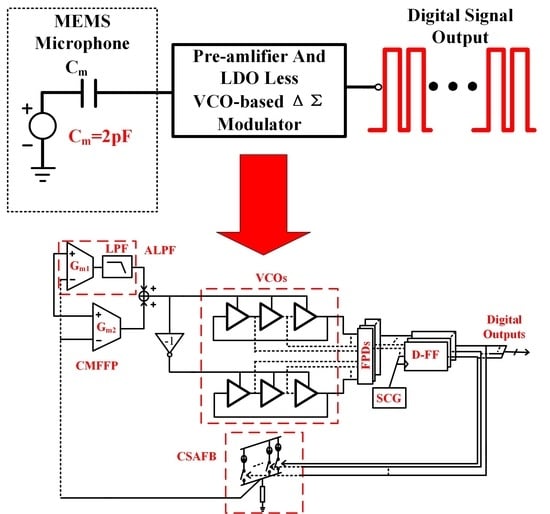
2.2. Proposed System Implementation

Figure 2 shows an equivalent microphone circuit and a proposed readout system. The equivalent circuit includes a microphone plate capacitor and a system interface capacitor (e.g., parasite capacitor or designed auxiliary capacitor). The readout system mainly consists of an LDO and PPA-less VCO-based delta-sigma modulator, a sampling clock generator (SCG) and current source array reference bias (CSARB).
The modulator shown in Figure 3 mainly consists of an ALPF, a CMFFP, a CSAFB, VCOs and frequency and phase detectors (FPDs). The ALPF provides partial open-loop gain for whole open-loop gain improvement and prevents input ripple from the phase gain of seriously degrading VCOs in order to improve signal accuracy. The CMFFP keeps the modulator loop stable within the gain-tuning range, while VCOs and FPDs convert voltage (from the ALPF) and current (from the CMFFP) signals into phase signals [27,28,29]. The SCG samples and outputs digital signals. With respect to PSRR performance, because of VCOs and the SCG phase variation robustness, the phase quantization is unchangeable with the variation in supply voltage. Therefore, the PSRR can be optimized without LDOs if phase-to-current control feedback is used. Thus, the CSAFB was designed and plays the role of a feedback network. Also, with current source control programmable in the CSAFB, the modulator loop feedback coefficient can be variable, so the gain can be tuned. Thus, the PPA can be free in the system.

2.3. Proposed System Mathematical Model

The corresponding transfer function model is shown in Figure 4. According to the mathematical model, the proposed loop transfer function can be given by:
G c l o s e _ l o o p = G o p e n _ l o o p 1 + f G o p e n _ l o o p
where G o p e n _ l o o p is the open-loop gain, and f is the feedback coefficient. The G o p e n _ l o o p can be given by as follows:
G o p e n _ l o o p = G 2 K V C O & P D s + G 1 1 + s ω p K V C O & P D s
where G 1 and G 2 are the ALPF and CMFFP gains, K V C O & P D is the voltage-to-phase gain coefficient of VCOs and FPD detector and ω p is a pole produced by the ALPF. It can be seen that open-loop gain is enhanced because of the ALPF gain G 1 .
According to the transfer function shown in Equation (2), the Bode diagram with and without the CMFFP is illustrated in Figure 5. Without the CMFFP, the feedback coefficient value range is limited within low values for the stability of the loop. With the CMFFP, a zero ω z is produced, and the feedback coefficient value range can be enhanced. Therefore, the gain-tuning range can be improved. On the other hand, as shown in Figure 5, because of the VCOs’ multi-outputs [27] and the CSAFB, feedback signal ripples can be minimized. Thus, the ALPF and CMFFP input stage trans-conductance can be kept at an approximate constant value.

2.4. Noise and THD

With respect to noise performance, according to the transfer function model, the ALPF and CMFFP are the first stages on the main signal path, and the CSAFB on the feedback path serves as the main noise contributing blocks. However, the CMFFP as an auxiliary gain block only provides a small gain. Therefore, it can be seen that since partial gain is provided by the ALPF, the noise contributed by VCOs and FPDs and CMFFP can be ignored. The system noise performance is mainly determined by ALPF and CSAFB blocks. The input-referred noise can be expressed as follows:
N o i s e i n 2 N o i s e A L P F 2 + N o i s e C S A F B 2
where N o i s e A L P F 2 and N o i s e C S A F B 2 are the ALPF and CSAFB input-referred A-weight density noise, respectively.
In addition, since audio signals are almost always in the lower frequency band, the 1/f noise of the device will greatly interfere with the signal transmission of the system. Due to the BCD process, high-performance BJT devices are easily available. The noise equivalent models of BJT and MOS devices are shown in Figure 6, where d v i e q t 2 ¯ is the equivalent input thermal noise voltage, d i i e q t 2 ¯ is the equivalent input thermal noise current, d v i e q f 2 ¯ is the equivalent input 1/f noise and d v i e q 2 ¯ is the total equivalent input noise ( d v i e q 2 ¯ = d v i e q t 2 ¯ + d v i e q f 2 ¯ ). The noise of MOS devices is mainly composed of thermal noise and 1/f noise, while BJT devices theoretically only contribute thermal noise. Since the 1/f noise of MOS devices at low frequency is quite large, a huge device size is required to reduce the 1/f noise. Since the 1/f noise of BJT devices is almost negligible compared to the MOS devices, the use of BJTs for key noise devices in the ALPF and CSAFB will greatly optimize the low-frequency noise performance of the entire system.
On the other hand, assuming that THD only refers to third-order distortion, THD can be given by [29]:
T H D ( α | V r i p p l e | + A i n ) 3
where V r i p p l e is ripple amplitude, α is THD equivalent coefficient induced by ripples and A i n is equivalent input base-band signals amplitude. It can be seen that in order to improve THD, the ALPF gain should be designed as high as possible, so A i n can be minimized. On the other hand, THD degrades with considerable ripple amplitude. Therefore, ripples should be minimized. According to the simulation, with the ALPF gain of 10 dB and ripple amplitude minimized into the level around 1 mV, THD within the bandwidth 100 Hz to 10 kHz achieves 70 dB@1 kHz, and THD degradation can be ignored. Thus, the −3 dB cut-off frequency provided by the ALPF can be approximately designed as follows:
f 3 d B f o s c × 10 2
where f o s c is the modulator-locked frequency.

2.5. PSR and Gain Tuning

With regard to PSR performance, due to the ring oscillator structure used in VCOs and SCGs, it is quite sensitive to power supply changes. There is a tail current source in the ALPF and CMFFP blocks, which have certain power supply rejection capabilities. Since two phase signals are outputted by VCOs and FPDs and quantized by the SCG, the PSRR of output digital signals can be approximately expressed as follows:
P S R R P R k S C G ( 1 P R k V C O s P R k S C G ) + P R F B F
where P R F B is the feedback path PSR ratio, F is the feedback coefficient and P R k V C O s and P R k S C G are PSR ratios of VCOs and SCG blocks in voltage-to-frequency domain, respectively. According to the equation above, it can be concluded that if P R k V C O s = P R k S C G and the CSAFB are designed in the feedback path, the output phase PSRR can be greatly improved. Since both VCOs and the SCG were designed with the same structure, they will have a similar PSR ratio, and P R k V C O s P R k S C G can be established. Furthermore, the PSRR can be further optimized if current source cascoded topology is used in the CSAFB. Thus, no extra LDOs need to be designed in the readout system.
On the other hand, the feedback coefficient can be regulated by means of controlling the current source array (CSA), so the readout system gain can be tuned. To achieve stability within the gain-tuning range, the CMFFP was designed, as shown in Figure 4. It converts microphone-sensed voltage into current and injects it into VCOs. Because of intrinsic current mode characteristic, voltage ripples can be neglected. The modulator gain-tuning range with and without the CMFFP is further noted as follows: Without the CMFFP, the open-loop phase margin is degrading with the decrease in modulator gain because of the ALPF and VCO poles. With the CMFFP producing a zero, phase margin can be compensated, so the gain-tuning range trade-off can be free. Therefore, compared with conventional systems [7,12], almost the same gain-tuning range can be achieved without designing an extra PPA.

3. Block Circuit Implementation

3.1. ALPF and CMFFP Implementation

As shown in Figure 7, the ALPF, unlike other conventional microphone interface circuits [30,31,32,33], consists of two source followers and a differential amplifier in order to achieve ultra-low input parasite capacitance. Furthermore, for high input impedance, source followers were designed with MOS input transistors. It can be seen from the previous noise considerations that using MOS devices in the input stage will produce large 1/f noise. However, in order to accommodate different MEMS sensor interfaces, large input impedance are necessary. Therefore, the size of the MOS device in the source follower can be appropriately increased to optimize the 1/f noise to achieve a compromise between area, noise and input impedance. Current tail sources are designed with bipolar transistors for flicker noise optimization. To filter out input ripples and realize signal amplification, the ALPF was designed with differential input stage source resistance feedback and parallel RC network loading impedance. On the other hand, the CMFFP was also implemented with a similar topology without loading impedance. It converts microphone-sensed signals into current signals, which are injected into output nodes of the VCOs V-I stage G m , as shown in Figure 7.

3.2. VCO and SCG Implementation

As shown in Figure 8, VCOs consist of the V-I stage G m and current controlled oscillators (CCOs). The V-I stage G m consists of input bipolar transistors and gate-to-drain shorted bipolar transistors with a current tail source for input-referred noise optimization and ground noise tolerance. The seven-stage CCOs succeed the V-I stage G m . Because of the ALPF filtering characteristic and CMFFP output connected to VCOs gate-to-drain shorted transistors, the voltage ripple can be ignored. Thus, VCO phase gain can be improved [29]. For oversampling and quantization robustness, the SCG is designed with the robust topology shown in Figure 9, and the SCG current source I b i a s 4 mirrors the CMFFP and V-I stage G m tail current sources. Considering phase quantization noise and power trade-off, the ratio of one-eighth between the VCOs and SCG frequency values is designed. By means of a simple negative feedback loop (consisting of four MOS transistors) shown in Figure 9, VCOs and the SCG power supply VDD are decoupled of the system VDD for further optimization of the system PSRR.

3.3. CSAFB and CSARB Implementation

Figure 10 shows that CSAFB consists of a bias current I b i a s 1 , current sources I U n i t 1 7 and RC loading impedance. The CSARB consists of a bias current I b i a s 2 , RC-matched impedance, a DC bias resistor R and an auxiliary capacitor C.
The CSAFB current source array (CSA) is controlled by digital multi-bits (sampled by the SCG), as shown in Figure 10. Initial ripple reduction can be achieved because of the multi-bit phase differences. Further ripple reduction can be realized with parallel RC network loading impedance. To design the gain-tuning function in the modulator, the current unit I U n i t 1 7 includes sub-current sources. Sub-current sources are designed to be different in order to achieve 2 dB gain steps. Unlike the bias reference circuit in other works [12,31,34,35,36], a bias current source I b i a s 2 and RC-matched impedance were designed in the CSARB in order to improve PSR and input mismatch performance. Combined with RC-matched impedance, the bias resistor Rbias provides DC bias for the whole readout system. The auxiliary capacitor C was designed to convert Δ C to Δ V as the system input signals. For the low input-referred flicker noise and high PSRR, current sources used in the CSAFB and CSARB are implemented with cascoded bipolar transistors.

4. Measurement Results

The proposed system is designed and fabricated with a 180 nm BCD process. The prototype is shown in Figure 11. The area is about 0.95 × 0.55 mm 2 . The system is measured at a 1.2 V supply voltage. To better evaluate the readout system, a test bench including the system and a circuit mimicking microphone sensitivity and electrical parameters [12,16,36,37] was designed, as shown in Figure 12. According to the simulation method in paper [12], C m = 2 pF was selected for this test bench, and the obtained open-loop sensitivity of the MEMS sensor was approximately −51.3 dBV/Pa.
The respective transient phase output signals at odd channels are shown in Figure 13. The respective approximate delta phase 2 π /7 demonstrates that the VCO output phase is locked, and voltage-to-phase conversion is achieved. At 40 dB gain, the system THD is measured within a 10 kHz bandwidth. If the gain is reduced, the bandwidth is expanded. As shown in Figure 14, the output swing is 0.8 V p p , and THD reaches −70 dB. Combined with noise performance, the corresponding SNDR is shown in Figure 15. It can be found that the peak SNDR of 62 dB and 65 dB is achieved with 40 dB and 20 dB gains, respectively. With the supply voltage sine wave swing amplitude of 200 m V p p @1.2 V, the PSRR at a 40 dB gain is shown in Figure 16. The PSRR achieves −55 dB@10 kHz. This means that the system achieves considerable power supply rejection capability without the need for an internal LDO. The respective block power at 20 dB gain (the maximum power achieved) is illustrated in Table 2. The total power is maintained within 57 µW, where VCOS, the SCG and FPDS occupy the main power consumption.
The performance and comparison with previous works are summarized in Table 3. According to the comparison, with the proposed technique, the accuracy and power performance in this work are superior (or comparable) to others, as shown in Table 3. On the other hand, design scalability is improved with the VCO-based modulator. In addition, no PPA or LDO is needed in the readout system. Therefore, compactness is also improved.

5. Conclusions

This paper presents a MEMS capacitive microphone digital readout system. The readout system is implemented with the LDO and PPA-less VCO-based Δ Σ modulation technique. The proposed technique improves system compactness and scalability. Moreover, the measurement results demonstrate that the accuracy and power performance are superior (or comparable) to other works because of the proposed technique. Therefore, the proposed system is well suited for low power and high accuracy applications.

Author Contributions

The contributions of the author of this paper are as follows: Conceptualization, F.L. and T.Y.; methodology, F.L.; validation, T.Y.; writing—original draft preparation, T.Y. and S.W.; writing—review and editing, S.W. and W.D. All authors have read and agreed to the published version of the manuscript.

Funding

This research was funded by National Natural Science Foundation of China (grant number 61974146) and Natural Science Foundation of Fujian Province, China (grant number 2021J01585).

Data Availability Statement

The data presented in this study are available on request from the corresponding author.

Conflicts of Interest

The authors declare no conflict of interest.

References

  1. Gemelli, A.; Tambussi, M.; Fusetto, S.; Aprile, A.; Moisello, E.; Bonizzoni, E.; Malcovati, P. Recent Trends in Structures and Interfaces of MEMS Transducers for Audio Applications: A Review. Micromachines 2023, 14, 847. [Google Scholar] [CrossRef] [PubMed]
  2. Fattaruso, J.; Hochschild, J.; Sjursen, W.; Fang, L.; Gata, D.; Branch, C.; Holmes, J.; Jiang, Z.; Chen, S.; Ling, K.; et al. Analog processing circuits for a 1.1 V 270 /spl mu/A mixed-signal hearing aid chip. In Proceedings of the 2002 IEEE International Solid-State Circuits Conference. Digest of Technical Papers (Cat. No.02CH37315), San Francisco, CA, USA, 7 February 2002; Volume 1, pp. 384–475. [Google Scholar] [CrossRef]
  3. Wu, J.; Fedder, G.; Carley, L. A low-noise low-offset capacitive sensing amplifier for a 50-/spl mu/g//spl radic/Hz monolithic CMOS MEMS accelerometer. IEEE J. Solid-State Circuits 2004, 39, 722–730. [Google Scholar] [CrossRef]
  4. Nebhen, J.; Savary, E.; Rahajandraibe, W.; Dufaza, C.; Meillère, S.; Haddad, F.; Kussener, E.; Barthélémy, H.; Czarny, J.; Walther, A. Low-noise CMOS analog-to-digital interface for MEMS resistive microphone. In Proceedings of the 2013 IEEE 20th International Conference on Electronics, Circuits, and Systems (ICECS), Abu Dhabi, United Arab Emirates, 8–11 December 2013; pp. 445–448. [Google Scholar] [CrossRef]
  5. van den Boom, J. A 50 μW biasing feedback loop with 6ms settling time for a MEMS microphone with digital output. In Proceedings of the 2012 IEEE International Solid-State Circuits Conference, San Francisco, CA, USA, 19–23 February 2012; pp. 200–202. [Google Scholar] [CrossRef]
  6. Arbet, D.; Nagy, G.; Kováč, M.; Stopjaková, V.; Nagy, L. Readout interface for capacitive MEMS microphone in CMOS technology. In Proceedings of the 2015 22nd International Conference Mixed Design of Integrated Circuits & Systems (MIXDES), Torun, Poland, 25–27 June 2015; pp. 370–374. [Google Scholar] [CrossRef]
  7. Chung, C.T.J.; Lu, C.C.; Rih, W.S.; Lee, C.F.; Shih, C.M.; Yeh, Y.L. An Ultra-low Power Voice Interface Design for MEMS Microphones Sensor. In Proceedings of the 2021 IEEE Sensors, Sydney, Australia, 31 October–3 November 2021; pp. 1–4. [Google Scholar] [CrossRef]
  8. Barbieri, A.; Nicollini, G. A 470 µA direct readout circuit for electret and MEMS digital microphones. Analog. Integr. Circuits Signal Process. 2014, 81, 229–240. [Google Scholar] [CrossRef]
  9. Picolli, L.; Grassi, M.; Fornasari, A.; Malcovati, P. A 1.0-mW, 71-dB SNDR, fourth-order ΔΣ interface circuit for MEMS microphones. Analog. Integr. Circuits Signal Process. 2011, 66, 223–233. [Google Scholar] [CrossRef]
  10. Jawed, S.A.; Cattin, D.; Massari, N.; Gottardi, M.; Baschirotto, A. A 1.8 V 828 µW 80 dB digital MEMS microphone. Analog. Integr. Circuits Signal Process. 2011, 67, 395–405. [Google Scholar] [CrossRef]
  11. Im, S.; Park, S.G. Analysis and Design of a Microphone Preamplifier for Mobile Applications. Electronics 2021, 10, 1624. [Google Scholar] [CrossRef]
  12. Yang, H.; Cho, J.S.; Yang, Y.; Kim, S. A load variation tolerant readout interface for high linear MEMS capacitive microphones. In Proceedings of the 2017 IEEE International Symposium on Circuits and Systems (ISCAS), Baltimore, MD, USA, 28–31 May 2017; pp. 1–4. [Google Scholar] [CrossRef]
  13. Yoo, Y.; Choi, B.D. Readout Circuits for Capacitive Sensors. Micromachines 2021, 12, 960. [Google Scholar] [CrossRef] [PubMed]
  14. InvenSense. T5837 Bottom Port PDM Digital Output Multi-Mode Microphone. Available online: https://invensense.tdk.com/download-pdf/t5837-datasheet/ (accessed on 23 May 2023).
  15. InvenSense. ICS-43434 Multi-Mode Microphone with I2S Digital Output Datasheet. Available online: https://invensense.tdk.com/download-pdf/ics-43434-datasheet/ (accessed on 23 May 2023).
  16. InvenSense. ICS-40310 Ultra-low Current, Low-Noise Microphone with Analog Output Datasheet. Available online: https://invensense.tdk.com/download-pdf/ics-40310-datasheet/ (accessed on 23 May 2023).
  17. Infineon. IM70A135V01 High Performance Analog XENSIV™ MEMS Microphone. Available online: https://www.infineon.com/cms/cn/product/sensor/mems-microphones/mems-microphones-for-consumer/ (accessed on 23 May 2023).
  18. Infineon. IM68A130V01 High Performance Analog XENSIV™ MEMS Microphone. Available online: https://www.infineon.com/cms/cn/product/sensor/mems-microphones/mems-microphones-for-consumer/ (accessed on 23 May 2023).
  19. Infineon. IM70D122V01 XENSIV™ Digital PDM MEMS Microphone. Available online: https://www.infineon.com/cms/cn/product/sensor/mems-microphones/mems-microphones-for-consumer/ (accessed on 23 May 2023).
  20. Nebhen, J.; Ferreira, P.M. A Chopper Negative-R Delta-Sigma ADC for Audio MEMS Sensors. CMES-Comput. Model. Eng. Sci. 2022, 130, 607–631. [Google Scholar] [CrossRef]
  21. Quintero, A.; Cardes, F.; Perez, C.; Buffa, C.; Wiesbauer, A.; Hernandez, L. A VCO-Based CMOS Readout Circuit for Capacitive MEMS Microphones. Sensors 2019, 19, 4126. [Google Scholar] [CrossRef] [PubMed]
  22. Maezawa, K.; Mori, M.; Andoh, H. Noise Floor Reduction in Frequency Delta-Sigma Modulation Microphone Sensors. Sensors 2021, 21, 3470. [Google Scholar] [CrossRef] [PubMed]
  23. Nikolić, M.; Florian, W.; Gaggl, R.; Liao, L. A 125dBSPL 1%-THD, 115 μA MEMS Microphone Using Passive Pre-Distortion Technique 2023. In Proceedings of the ESSCIRC 2023—IEEE 49th European Solid State Circuits Conference (ESSCIRC), Lisbon, Portugal, 11–14 September 2023; pp. 209–212. [Google Scholar] [CrossRef]
  24. Lee, B.; Yang, J.; Cho, J.S.; Kim, S. A Low-Power Digital Capacitive MEMS Microphone Based on a Triple-Sampling Delta-Sigma ADC With Embedded Gain. IEEE Access 2022, 10, 75323–75330. [Google Scholar] [CrossRef]
  25. Silva, J.; Moon, U.; Steensgaard, J.; Temes, G.C. Wideband low-distortion delta-sigma ADC topology. Electron. Lett. 2001, 37, 737–738. [Google Scholar] [CrossRef]
  26. Verma, N.; Chandrakasan, A.P. An Ultra Low Energy 12-bit Rate-Resolution Scalable SAR ADC for Wireless Sensor Nodes. IEEE J. Solid-State Circuits 2007, 42, 1196–1205. [Google Scholar] [CrossRef]
  27. Li, S.; Mukherjee, A.; Sun, N. A 174.3-dB FoM VCO-Based CT ΔΣ Modulator With a Fully-Digital Phase Extended Quantizer and Tri-Level Resistor DAC inshould be a space130-nm CMOS. IEEE J. Solid-State Circuits 2017, 52, 1–13. [Google Scholar] [CrossRef]
  28. Gutierrez, E.; Hernandez, L.; Cardes, F.; Rombouts, P. A Pulse Frequency Modulation Interpretation of VCOs Enabling VCO-ADC Architectures with Extended Noise Shaping. IEEE Trans. Circuits Syst. Regul. Pap. 2018, 65, 444–457. [Google Scholar] [CrossRef]
  29. Fanyang, L.; Shuying, C. A Highly Digital ADC with Enhanced Accuracy Using a Simple Ripple-Transferring Replica Pseudo PLL Loop Technique. IEEE Trans. Circuits Syst. II Express Briefs 2018, 66, 197–201. [Google Scholar] [CrossRef]
  30. Jawed, S.A.; Nielsen, J.H.; Gottardi, M.; Baschirotto, A.; Bruun, E. A multifunction low-power preamplifier for MEMS capacitive microphones. In Proceedings of the Esscirc, Athens, Greece, 14–18 September 2009. [Google Scholar]
  31. Barbieri, A.; Nicollini, G. 100+ dB A-Weighted SNR Microphone Preamplifier with On-Chip Decoupling Capacitors. IEEE J. Solid-State Circuits 2012, 47, 2737–2750. [Google Scholar] [CrossRef]
  32. Oh, S.; Jang, T.; Choo, K.D.; Blaauw, D.; Sylvester, D. A 4.7uW switched-bias MEMS microphone preamplifier for ultra-low-power voice interfaces. In Proceedings of the Symposium on Vlsi Circuits, Kyoto, Japan, 5–8 June 2017. [Google Scholar]
  33. Jawed, S.A.; Cattin, D.; Gottardi, M.; Massari, N.; Baschirotto, A. A low-power interface for the readout and motion-control of a MEMS capacitive sensor. In Proceedings of the IEEE International Workshop on Advanced Motion Control, Trento, Italy, 26–28 March 2008. [Google Scholar]
  34. Cheng, A. Design of a Readout Scheme for a MEMS Microphone. Electr. Eng. Math. Comput. Sci. 2009. [Google Scholar]
  35. Citakovic, J.; Hovesten, P.F.; Rocca, G.; van Halteren, A.; Rombach, P.; Stenberg, L.J.; Andreani, P.; Bruun, E. A compact CMOS MEMS microphone with 66 dB SNR. In Proceedings of the 2009 IEEE International Solid-State Circuits Conference—Digest of Technical Papers, San Francisco, CA, USA, 8–12 February 2009; pp. 350–351. [Google Scholar] [CrossRef]
  36. Ersoy, S.; van Veldhoven, R.H.; Sebastiano, F.; Reimann, K.; Makinwa, K.A. A 0.25mm2 AC-biased MEMS microphone interface with 58dBA SNR. In Proceedings of the 2013 IEEE International Solid-State Circuits Conference Digest of Technical Papers, San Francisco, CA, USA, 17–21 February 2013; pp. 382–383. [Google Scholar] [CrossRef]
  37. Resources, T.I.D. Speech Recognition Reference Design on the C5535 eZdspTM. Available online: https://www.ti.com/tool/TIDEP0066 (accessed on 23 May 2023).
Figure 1. The conventional microphone readout system.
Electronics 12 05014 g001
Figure 2. The proposed readout system.
Electronics 12 05014 g002
Figure 3. Topology of the proposed modulator.
Electronics 12 05014 g003
Figure 4. The corresponding transfer function model.
Electronics 12 05014 g004
Figure 5. The Bode diagram of the open loop and the illustration of the feedback single-bit and multi-bit signals.
Electronics 12 05014 g005
Figure 6. Device noise equivalent model.
Electronics 12 05014 g006
Figure 7. ALPF and CMFFP implementation.
Electronics 12 05014 g007
Figure 8. VCO implementation.
Electronics 12 05014 g008
Figure 9. SCG implementation.
Electronics 12 05014 g009
Figure 10. CSAFB and CSARB implementation.
Electronics 12 05014 g010
Figure 11. Proposed readout system prototype.
Electronics 12 05014 g011
Figure 12. Readout system test bench.
Electronics 12 05014 g012
Figure 13. Transient measurement of the FPDs output signals.
Electronics 12 05014 g013
Figure 14. THD of readout system output signals.
Electronics 12 05014 g014
Figure 15. SNDR performance at 20 dB and 40 dB gain.
Electronics 12 05014 g015
Figure 16. Readout system PSRR performance at 40 dB gain.
Electronics 12 05014 g016
Table 1. The mainstream products of several influential companies.
ProductProducerTypical Voltage (V)Typical Current (µA)SNR (dBA)Output TypeTopology
T5837 [14]InvenSense1.831068DigitalLDO + ADC + PDM
ICS-43434 [15]InvenSense1.8/3.331065DigitalLDO + ADC + I 2 S
ICS-40310 [16]InvenSense0.9–1.319.564AnalogLDO + Amplifier
IM70A135 [17]Infineon1.5–3.017070AnalogLDO + Amplifier
IM68A130 [18]Infineon2.4–3.611068AnalogLDO + Amplifier
IM70D122 [19]Infineon1.6–3.698070DigitalLDO + ADC + PDM
Table 2. Power performance (gain = 20 dB).
BlocksPower (µW)
ALPF9
VCOS, SCG and FPDS∼23
CMFFP∼8
CSAFB∼9
CSARB8
Whole System57
Table 3. Performance summary and comparison.
Ref#[4][7][12][32][36]This Work
Process280 nm180 nm180 nm180 nm160 nm180 nm
VDD (V)2.51.23.31.44.0∼6.01.2
Area (mm 2 )10.4020.550.070.250.52
THD @1 kHz
(%@dB SPL)
/0.25@94/0.6@940.5@940.035@94
Input-referred noise8 nV/sqrHz2.6/5.7 µ V rms /7.3 µ V rms ∼30 nV/sqrHz∼10 nV/sqrHz
Power (µW)2400<154500∼15,00052000∼3000<57
Gain range (dB)6522∼40−7.88 ∼11.819.6/20∼40
MEMS sensitivity (dBV/Pa)/−37−53−29.5−35.1−51.3
Output signal typeDigitalDigitalAnalogAnalogAnalogDigital
TopologyPre-amplifier + Δ Σ ADCPre-amplifier + SAR-ADCPre-amplifierPre-amplifierPre-amplifierVCO-based Δ Σ
Disclaimer/Publisher’s Note: The statements, opinions and data contained in all publications are solely those of the individual author(s) and contributor(s) and not of MDPI and/or the editor(s). MDPI and/or the editor(s) disclaim responsibility for any injury to people or property resulting from any ideas, methods, instructions or products referred to in the content.

