2. Materials and Methods
The fundamental aim of this study is to investigate the distribution of Joule heating induced by variations in the area ratio between the metal line and via. To comprehensively explore this phenomenon, this study harnesses the powerful capabilities of the Ansys simulator (
https://www.ansys.com), a widely respected and extensively used software tool in the realm of engineering simulations [
16,
17]. The selection of this advanced simulation platform ensures the accuracy and validity of the experimental outcomes, laying a robust foundation for the subsequent analysis.
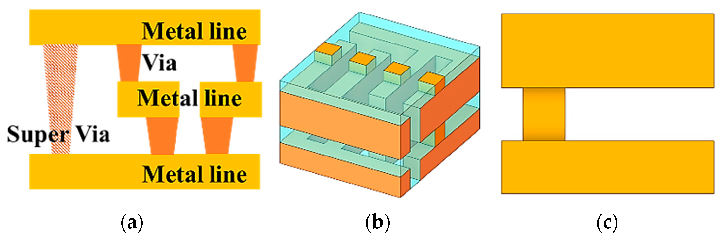
As revealed in
Figure 1b, the BEOL structure is meticulously brought to life within the simulator’s virtual environment. By faithfully replicating real-world conditions, this simulation approach bridges the gap between theoretical predictions and practical scenarios, fostering a deep understanding of the system’s behavior under varying conditions. Efforts to achieve efficiency in research outcomes while retaining their relevance led to the creation of a simplified model. This model captures the essential aspects of the complex BEOL structure while streamlining its complexity. By focusing on the core attributes that significantly impact power transmission and reliability, the model preserves the fundamental characteristics that warrant investigation. This simplified representation is illustrated in
Figure 1c, where the upper metal line, lower metal line, and connecting via are distilled into a visually digestible form. This model serves as the canvas on which the intricate dance of Joule heating and thermal dynamics is painted, enabling insightful interpretations and actionable conclusions.
Incorporating the concept of interconnect simplification is a strategic decision that magnifies the clarity of the study’s findings. This intricate network of components, encapsulating the upper metal line, lower metal line, and the connecting via, forms the cornerstone of modern microelectronics. The connection configuration of the metal line and via (plug) is not only used in the BEOL structure but also extends to the area between bumps and pads. Moreover, it is the same structure used in the interposer region associated with chip packaging technology, with only different names. The configuration, which involves connecting two different signal transmission layers orthogonally with plugs, serves as the fundamental structure for signal and power delivery in semiconductor systems. Therefore, the simplified structure can be expanded and applied across the entire spectrum of the semiconductor system, not limited to the BEOL area.
Figure 1c provides an insightful visualization of these elements, seamlessly illustrating their roles in power transmission and signal propagation. The synergistic interaction among these components governs the overall efficiency and reliability of the system, making it imperative to dissect their individual contributions to the thermal phenomenon under investigation.
This study conducted FEM analysis using analysis tools within Ansys (Simulator). The employed analysis tools included electric and steady-state thermal, each conducted as separate projects, and they were interlinked. When configuring the size of the simulation structure, we referred to the specifications of bumps and metal lines produced at the current process level. Bumps are typically manufactured with micro bump standards, approximately 20 μm in size, while metal lines, when positioned directly above transistors, have line widths in the range of ~20 nm [
18,
19]. Therefore, between the transistor and the bump, there are multiple layers of metal lines with line widths ranging from 20 nm to 20 μm. The connection between the bump and metal line ultimately has the same form, where it connects the upper metal and lower metal with a plug. Among these, we used the 20 μm line width as a reference and based our research on metal lines with widths of 15 μm and 30 μm as the standard for simulation specifications. The Joule heat values obtained from electric analysis were used as inputs within the simulation to derive temperature results in the steady-state thermal analysis, considering various material properties. To delve into specifics, the simulation model incorporated Cu alloy properties (isotropic elasticity with 1.1 × 10
5 MPa Young’s modulus and 0.34 Poisson’s ratio, isotropic thermal conductivity with 4.01 × 10
8 pW/μm·°C, and isotropic electric resistivity with 16.94 MΩ·μm at 20·°C) provided by Ansys Simulation for the metal line and via. After selecting the material, we configured the Mesh conditions for precise calculations. The chosen model, which is the BEOL structure, plays a critical role in receiving power and electrically transmitting input signals. In the case of our research target, high-power components within the BEOL structure experience elevated power densities, resulting in the generation of Joule heat. Consequently, the interconnect is subjected to extreme temperatures, leading to defects and reduced reliability. To accurately analyze the vulnerabilities of this BEOL structure and temperature effects caused by Joule heat, we set up a mesh consisting of 219,000 cubic elements with a width of 0.5 μm across the entire sample model. Each mesh element undergoes individual calculations, providing us with the desired results, including current density and Joule heat experienced by the sample, based on material properties, applied currents, and sample volume. Based on approximately 200,000 meshes, the time required to extract current density, Joule heating, and temperature changes in individual mesh units in this structure is approximately 5 min, allowing for the simulation of roughly 40,000 meshes per minute. While the relative simplicity of the structure composed of metal lines and vias contributes to this efficiency, it is worth noting that if we had conducted the same analysis by creating actual samples and measuring their electrical and thermal properties, it would have taken several days. Therefore, utilizing a simulation proved to be a highly efficient approach for our research. In essence, if the current level is known, it is possible to determine the ratio of metal line width to via width based on simulation results, ensuring that it does not compromise reliability.
Once the mesh settings were completed, we configured the electrical settings for the analysis. We conducted a total of three simulations, all aimed at comparing and analyzing trends in heat distribution based on the area ratio between metal lines and vias. It is important to note that these simulations were not meant to replicate real-world conditions but, rather, to find the optimal area ratio. To achieve this, we excluded the actual melting point (~1084 °C) and boiling point (~2562 °C) of the materials used, as they were not relevant to our analysis. As depicted in
Figure 2 in the paper, the applied current flows from the top metal, passes through the via, and reaches the bottom metal with the specified ground voltage (0 V). This current is calculated within each pre-defined mesh element, producing the desired results, including total current density and Joule heating values.
In this study, our primary focus was on the thermal analysis of vias, which is why the thermal analysis was conducted as the final step. The two analysis tools are interconnected, with Joule heat values from the electric analysis converted into temperature in the thermal analysis. Similar to the electric analysis, we configured the settings for the thermal analysis. In the case of convection, the entire model was set as a boundary condition to analyze the heat generated by Joule heat due to the current flowing through the metal line and via. We used the stagnant air-simplified case (5 pW/μm2·°C) provided by Ansys as the import convection data. The ambient temperature was set to 22 °C, which is room temperature. With these settings, the solution was applied to calculate the temperature, considering Joule heat values from the electric analysis, material properties of the Cu alloy, and the volume of the entire model. In this study, we identified the vulnerable areas where the metal line and via experienced extreme temperatures and used these as the temperature limits for the simulation. Therefore, we built the data for the temperature distribution trends in the model structure using only the maximum values from the simulations. (1) Comparison analysis of area ratio (1~15) between metal lines and vias for two samples with widths of 15 μm and 30 μm, respectively (applied current: 10 mA for the 15 μm width sample, 40 mA for the 30 μm width sample). (2) Comparison analysis of area ratio (1~15) within the 30 μm width sample structure under different applied currents (20 mA, 40 mA, 60 mA) from Simulation 1. (3) Comparison analysis of area ratio (1~15) for the 15 μm width sample with varying heights of the top metal (15 μm, 30 μm, 60 μm) under an applied current of 10 mA.
3. Results
In this study, as previously mentioned, an analysis was meticulously conducted through simulations to comprehensively investigate the reliability degradation resulting from heat generation due to the flow of current through vias of varying sizes. Research on the reliability of BEOL structures is relatively limited compared to FEOL and packaging studies. Even the existing research primarily focuses on material or process optimization activities, and there is a shortage of results that can provide practical guidance for the design of actual interconnect structures [
20,
21].
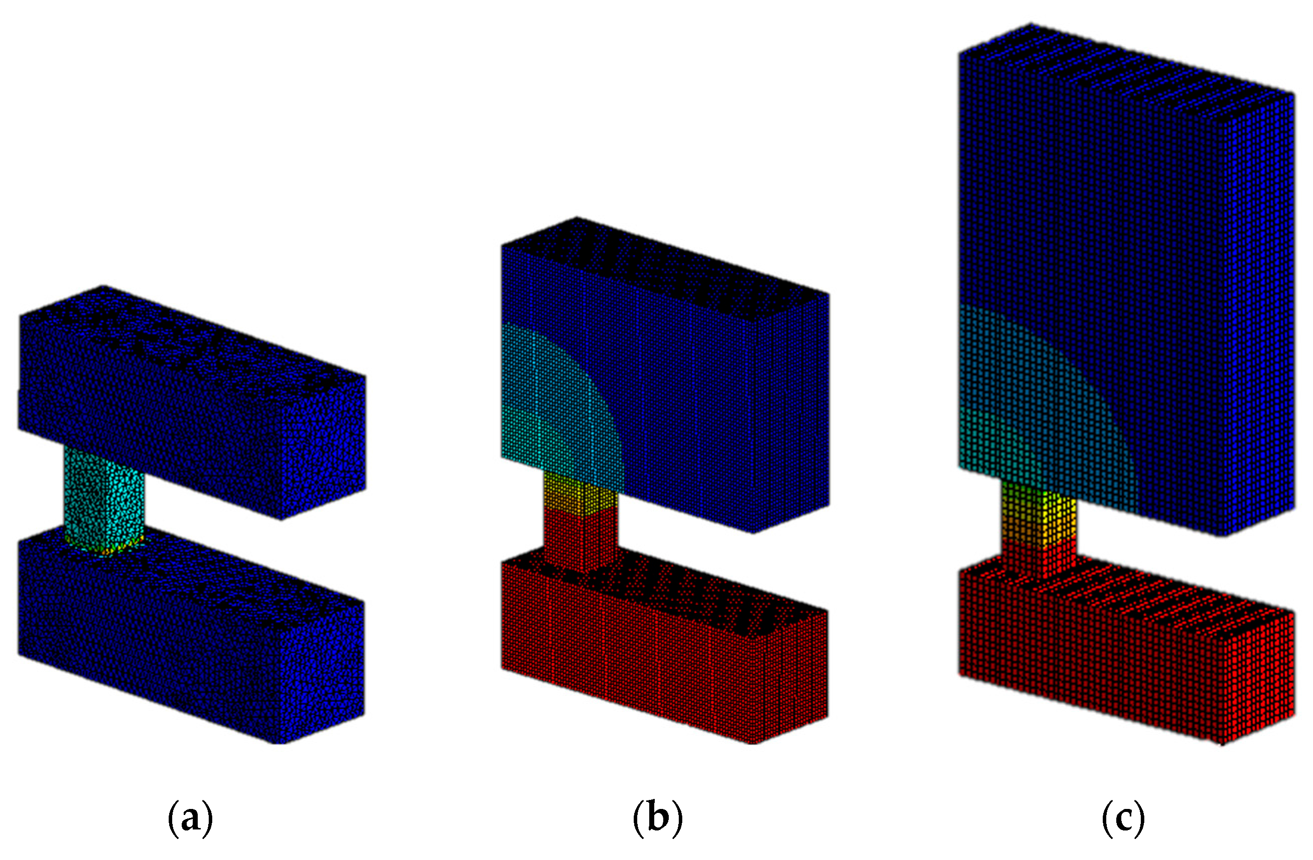
Figure 2 serves as an illustrative example of the simulation results, showcasing the impact of the via dimensions on the temperature distribution and subsequent reliability concerns.
The structural configuration was designed in such a way that current is injected into the upper metal line while being extracted from the lower metal line. This configuration allowed us to delve into the intricate details of the simulation outputs within the Ansys environment. The simulation allows for thermal analysis of structures implemented using various parameters [
22]. Its outcomes encompass a spectrum of parameters, including current density, heat distribution attributed to Joule heating, and the resulting temperature changes across different spatial regions. The comprehensive nature of these results provides extensive insight into the complex interplay between various factors that influence the behavior of the interconnect structure. As shown in
Figure 2a,b, the gradual modification of the via size unveils the intricate relationship between dimensions and temperature profiles across distinct regions, reinforcing the need for a nuanced approach in interconnect design to ensure optimal performance and reliability.
Figure 2c provides a zoomed-in perspective, specifically focusing on the via region. This detailed view offers a deeper understanding of the temperature distribution across different mesh points, shedding light on the local variations in temperature and other critical parameters.
To investigate the reliability of the via, particularly the factors influencing the temperature rise when signals are applied, we examined how temperature varies with the area ratio between the metal line and via (ranging from 1 to 15). We conducted simulations to explore the impact of input current magnitude, the influence of input line size while maintaining current density, and the effects of input line size while keeping via current density constant. These simulations were conducted with a baseline temperature set at room temperature (22 °C). Initially, we performed a simulation to understand how the temperature variation caused by Joule heating in the via, when current flows through both the metal line and the via, is affected by scaling down.
Figure 3 presents the results of this simulation. Scaling down primarily involves reducing the sizes of the via and the metal line. As the size decreases from the upper metal line to the lower metal line, the dimensions gradually diminish, including that of the connecting via. In other words, in a scaled-down system, forming a smaller via allows them to be connected to a smaller lower metal line. Therefore, it was essential to analyze the impact of the size of the via on heat generation. To do so, we examined the extent of heat generation based on the area ratio of the via in contact with the metal line.
To perform the simulation, the baseline dimensions of the metal line were set to 15 μm (width and height), and the via was gradually reduced in size in the form of a square prism, with one side of the cross-section starting at 15 μm. When the metal line and via fit perfectly without any gaps (where the width of the metal line is 15 μm and the length of one side of the via is also 15 μm), it was defined as area ratio 1. Here, we progressively reduced the size of the via while varying the area ratio (the area of the metal line relative to the cross-sectional area of the via) up to 15. This allowed us to examine the temperature changes in the via caused by the flow of current.
Figure 3a provides an in-depth analysis of how the dimensions of the metal line influence the system. In this investigation, we carefully set the width and height of the metal line at 15 μm and 30 μm, respectively, while maintaining uniform current density applied to the metal line. This allowed us to closely examine the temperature variations within the via, primarily focusing on the area ratio as our variable of interest. The graphical representation reveals a distinctive second-degree polynomial pattern. In the case of metal lines in semiconductor systems, research has shown that increasing the width can reduce stress [
23]. However, for vias, such research findings do not exist. Even if we were to apply similar results, vias are more challenging to size according to the designer’s preferences because they are subject to size constraints imposed by the specifications of the upper and lower metal lines. Nevertheless, by confirming the presence of a second-degree polynomial pattern here, we can deduce that as the size ratio between the metals decreases, the temperature rise becomes progressively more severe. Therefore, it can be concluded as a preliminary observation that the specifications for vias cannot be arbitrarily reduced. At an area ratio of approximately three, we note a significant turning point where the temperature effectively doubles. This intriguing pattern suggests a critical threshold point in the relationship between the area ratio and temperature amplification within the via. Delving deeper into our findings, an intriguing insight comes to light. Even when we maintain a consistent area ratio, such as in the case of the wider metal line with dimensions of 30 μm for both width and height, we encounter elevated temperatures within the via. However, it should be noted that when the overall system specifications (metal line and via) change in conjunction with the current, the temperature rise does not exhibit a proportional relationship with the current. This observation raises an important consideration: the overall current magnitude plays a pivotal role in determining the thermal behavior of the interconnect system. In essence, our experiments underscore that the total amount of current significantly influences the system’s overall temperature, and this effect persists even when we rigorously uphold uniform current density as a constant parameter.
To more deeply explore the impact of current magnitude, we adhered to a rigorous experimental protocol. In this rigorously controlled study, we kept the dimensions of both the metal line and the via constant, maintaining a width of 15 μm and a height of 30 μm. However, we introduced a variable that held the key to unraveling the intricate relationship between the current magnitude and temperature behavior: the current magnitude itself. Incrementally, we augmented the current magnitude by three distinct levels: 20 mA, 40 mA, and 60 mA. This allowed us to adopt a more granular perspective when scrutinizing the effects of varying current magnitudes. The results, as depicted in
Figure 3b, unveiled a pattern that echoed our earlier discoveries. Specifically, as the current magnitude steadily increased, we once again encountered a temperature rise conforming to a second-degree polynomial function, mirroring our prior observations.
Notably, an intriguing revelation surfaced when we examined the data closely. When the overall current was elevated to higher levels, the graph exhibited a noticeable upward shift. Furthermore, when keeping the specifications consistent, we observed that the temperature rise is proportional to the square of the overall current; in other words, it is proportional to the square of the current density within the via (when the current doubles, the temperature rise increases by a factor of four, and when the current triples, the temperature rise increases by a factor of nine). This shift was a clear indicator of the interconnect system reaching higher temperatures, even in the context of intensified Joule heating factors induced by the augmented overall current. Interestingly, this phenomenon echoed a parallel occurrence we had observed previously: a substantial doubling of temperature centered around an area ratio of approximately three. This recurrent observation underscores the potential risks associated with this specific ratio, which appear to persist across varying experimental conditions.
The recurring manifestation of this phenomenon, regardless of the conditions, underlines its robustness and its critical role in governing the thermal behavior of the system. Our systematic investigation, which thoroughly examined the interplay between current magnitude and area ratio, has provided us with comprehensive insights. Through a meticulously controlled manipulation of current variables and a rigorous analytical approach, we have consistently unveiled trends indicative of a second-degree polynomial temperature escalation. These trends, as we have come to understand, are often clustered around the area ratio of approximately three. Furthermore, it becomes increasingly evident that the effects of the current magnitude accentuate these trends, reaffirming their profound significance in shaping the overall performance and thermal behavior of the interconnect system.
We did not just aim to find the point where the temperature doubles; rather, we sought to determine a practical criterion for the occurrence of defects in interconnects using metal due to thermal stress. By combining the results of multiple papers, we found that reliability could be affected starting from around ~150 °C [
24,
25,
26,
27]. Furthermore, by refining the temperature change graph based on the area ratio (
Figure 2 and
Figure 3), a formula
can be obtained. In other words, if we take 150 °C as the reference temperature, doubling the input current would require doubling the via width to prevent any additional temperature increase. Based on the formula, when 40 mA of current flows through a 30 μm wide metal line, resulting in a temperature of 150 °C, the area ratio is approximately three (indicating a via width of 10 μm). If the current is reduced to 20 mA, halving it, we can expect the via to also be halved, allowing for scaling down to 5 μm with an area ratio of ~six, which aligns with the simulation results. Similarly, when 10 mA of current flows through a 15 μm wide metal line, reaching a temperature of 150 °C, and then the current is reduced to 20 mA (halved), we can anticipate the via being halved to 2.5 μm (with an area ratio of ~six), which is also consistent with the graph.
Upon examining the results from the previous
Figure 2 and
Figure 3, it became evident that, ultimately, an increase in the total current applied to the system, even with the same current density flowing through the via, leads to comparatively higher heat generation. On the basis of this insight, we speculated that, even with consistent current density in the via, reducing the overall current flowing through the system could potentially mitigate the temperature rise within the via. Therefore, we sought to find an interconnect structure that could enhance the reliability of the via based on the simulation method described earlier.
To achieve a reduction in the overall current while maintaining consistent current density within the via, one possible approach is to decrease the current density in the metal line. In other words, the input current into the metal line remains the same, but by altering certain specifications, the current flow per unit area is decreased. However, it is important to note that in semiconductor interconnect structures, the width and spacing of lines are typically determined so as to meet the specifications of the entire system. Therefore, changing the width of the lines may not be a feasible option. As a more practical alternative, we considered increasing the height of the metal line during the structure formation process through patterning and deposition techniques. This adjustment would effectively reduce the current density flowing through the metal line while keeping the metal line’s width unchanged. We proceeded with simulations while making such structural changes in this direction.
Figure 4 depicts the structure used for the mentioned simulations. Building upon a structure with a metal line width of 15 μm, we increased the height to 15 μm, 30 μm, and 60 μm, following the previous simulation approach to observe temperature changes based on the area ratio in the interconnect structure, similar to the results obtained earlier. The input current values into the interconnect structure remained consistent. As the height increased, the current density in the metal line decreased, while the current density flowing through the via remained constant.
Figure 5 presents the outcomes of the simulations conducted using the structure from
Figure 4. Similar to the results of the previous simulations, all the results show a temperature increase based on the area ratio, displaying a second-degree polynomial pattern. Furthermore, there is a consistent trend of the temperature doubling around an area ratio of approximately three, compared to the initial temperature at an area ratio of one, as observed in the earlier simulations.
However, there are some notable differences in these results. As anticipated, an increase in the height of the metal line leads to a decrease in both the initial temperature and the temperature rise. This trend becomes more pronounced at heights of 30 μm and 60 μm. When the width of the metal line is maintained at 15 μm and only the height is increased from 15 μm to 30 μm, the temperature rises within the via decrease, but the absolute difference remains relatively minor, around 8 °C, despite doubling the height. However, when the height is doubled from 30 μm to 60 μm (which is four times the height of the 15 μm model), a consistent approximately two-fold reduction in temperature across various area ratios is observed. These findings highlight that increasing the height of the metal line—effectively lowering the current density within the metal line—gradually and significantly reduces the Joule heating generated within the via. Consequently, this substantially suppresses temperature rise effects.
The Joule heating responsible for the temperature rise in the via is generated by the interaction between the moving charge carriers (electrons) and the atomic ions that make up the conductor. Electrons are accelerated by the electric field, but they lose kinetic energy with each collision with ions. Conversely, the energy of ions increases through these interactions. As a result, the kinetic or vibrational energy of ions translates into heat, leading to an increase in the temperature of the conductor (via). Considering this in connection with the causes of Joule heating, even when the current density in the via is the same (i.e., the current flowing through the upper metal line connected to the via is the same), when the current density in the upper metal line is lower, it can be inferred that the acceleration of electrons is relatively reduced. The key parameters related to the energy transferred by electrons in collisions with ions include the quantity and velocity of electrons. Since the quantity of electrons is the same, the only variable that can lead to differences is velocity. Even with the same quantity of electrons, the reduced acceleration results in less energy transfer during collisions with ions, leading to a lower temperature rise as a consequence.
Furthermore, because this trend does not exhibit linearity, it has also been confirmed that increasing the thickness of the metal line to the maximum extent allowed by the process and BEOL specifications can progressively enhance the overall reliability of the entire interconnect system. This can be considered valuable standardized guidance for improving the reliability of semiconductor interconnect systems in research related to enhancing reliability.


