Article

A Multi-Beam XL-MIMO Testbed Based on Hybrid CPU-FPGA Architecture

National Mobile Communications Research Laboratory, Southeast University, Nanjing 210096, China
*
Author to whom correspondence should be addressed.
Electronics 2023, 12(2), 380; https://doi.org/10.3390/electronics12020380
Submission received: 5 December 2022 / Revised: 4 January 2023 / Accepted: 6 January 2023 / Published: 11 January 2023
(This article belongs to the Special Issue Extremely Large-Scale MIMO for 6G Wireless Transmission)

Abstract

:
To support more users and higher data rates in future communication networks, the extremely large-scale massive multiple-input multiple-output (XL-MIMO) is considered a promising technique. The booming research on XL-MIMO necessitates a reconfigurable XL-MIMO testbed that can be used to validate new research ideas in real wireless environments and collect data for XL-MIMO channel characteristics analysis. To provide such a reliable and convenient testbed, we designed a multi-beam XL-MIMO testbed based on the hybrid CPU-FPGA architecture and channel calibration schemes. The ability to customize modules makes our testbed a convenient verification platform for future communication systems. Moreover, numerous trial measurement results in the indoor near-field scenario with moderate user equipment (UE) mobility are presented, and the excellent performance indicates that our testbed is an ideal platform for the evaluation of XL-MIMO-related algorithms.

1. Introduction

With the rapid increase in the number of smart devices and the rise of emerging applications such as virtual reality and smart cities, future networks are expected to support more users and higher data rates. Compared to massive multiple-input multiple-output (MIMO), extremely large-scale multiple-input multiple-output (XL-MIMO) with much more antennas can provide higher spectral efficiency, and are thus regarded as one of the key techniques in future communications.
However, the evolution from massive MIMO to XL-MIMO means not only a change in the number of antennas, but also a fundamental change in the electromagnetic (EM) field characteristics. In the XL-MIMO systems, the Rayleigh distance, which is the boundary between near-field and far-field transmission, is not negligible compared to the distance between the base stations (BSs) and user equipments (UEs) [1,2]. Therefore, the array will experience a spherical wavefront instead of a planar wavefront, and the angle of arrival/departure (AoA/AoD) between the BSs and UEs vary over the array [3]. Moreover, the beamforming technique is applied in XL-MIMO systems to concentrate power in angle domain. Thus, fine beam alignment is required, which is achieved by the procedure known as beam management. Generally, the procedure consists of two steps: (1) initial access procedure for idle users [4,5], which allows mobile UEs to establish communication links with BSs; (2) beam tracking procedure [6], which is used for communication links maintenance during the mobility of UEs.
Many algorithms, including baseband signal processing algorithms and array processing algorithms, are based on ideal assumptions that usually do not exist in realistic scenarios, resulting in the potential deterioration of algorithm performance. Thus it is essential to implement new research ideas on testbeds and examine their performance in real-world environments [7]. On the one hand, the performance of testbeds should be excellent enough to support the evaluation of a variety of algorithms. On the other hand, the testbed should allow the researchers to custom the waveforms, frame structures, coding and modulation schemes and other modules to provide convenience for algorithm verification. In other words, the testbed architecture should be flexible and scalable enough through modular design and parametric design, which contributes to the examination of techniques of future communication systems.
Having realized the importance of testbeds, several testbeds have been implemented to confirm the potential of critical techniques for future communication systems. For example, in [8,9,10,11] massive MIMO testbeds deployed in the sub-6G band was implemented, while in [12,13,14] mmWave massive MIMO testbeds with 20 MHz bandwidth was implemented. Furthermore, the 5G NR-based end-to-end mmWave testbed with hybrid beamforming architecture was implemented in [15,16], but the universal software radio peripherals with reconfigurable I/O (USRP-RIO) used in the testbeds only support a maximum bandwidth of 120 MHz. From the above review, it is obvious that existing testbeds either only support sub-6 GHz bands, or only support narrow-band communication in mmWave bands, or only support one beam, which cannot meet the requirements of massive users and high data rate transmission. In addition, they have yet to implement an XL-MIMO testbed. To address these limitations, we are determined to develop a testbed that supports a maximum bandwidth of 400 MHz and the verification of various baseband algorithms in XL-MIMO communication with hybrid beamforming architecture, which is conducive to the follow-up research. On the one hand, the testbed can collect data received by the phased array antenna so that it can be used for channel characteristics measurements, including broad-band effects and near-field effects, which will contribute to the research of XL-MIMO channel models and other XL-MIMO-related algorithms. On the other hand, the testbed can be easily reproduced by other research groups and used for the evaluation of various algorithms in real-world environments due to its modular and parametric design. The detailed characteristics of our testbed are as follows:
1.
Multiple beams: In our testbed, a maximum of eight beams are supported and can be further expanded. Moreover, calibration of amplitude and phase deviations, which are caused by phased array antennas, analog-to-digital converters (ADCs) and cables with different lengths, are implemented. Thus, algorithms corresponding to multi-user scenarios can be evaluated using our testbed.
2.
The flexible and fast deployment of high-throughput baseband algorithms: The field programmable gate array (FPGA) can realize high-speed data processing while the developing period is long, as opposed to x86 servers. Thus, FPGA and x86 servers are combined to support the fast deployment of arbitrary algorithms. Moreover, our test platform adopts a modular and parametric design, which enables the customization of different algorithms, waveforms and parameters.
3.
The mmWave band and broad bandwidth: The operating carrier frequency and signal bandwidth are 28 GHz and 400 MHz, respectively, so that the testbed can be used for the evaluation of algorithms related to broadband mmWave signal and measurement of broadband mmWave channel characteristics.
4.
Flexible beam patterns: In our testbed, various desired beam patterns can be achieved by adjusting the phase shifter on each antenna element, which contributes to the evaluation of different beamforming algorithms.
The rest of the paper is organized as follows. In Section 2, the general architecture of our testbed is overviewed. In Section 3, we give an example of our testbed, where system parameters definition, frame structures and specific modules are described. Some experiments are performed in Section 4, and the experimental results are presented. Some conclusions are given in Section 5.

2. System Architecture

In this section, an overview of the top-level architecture of our testbed is introduced, followed by the channel calibration operation and software architecture.

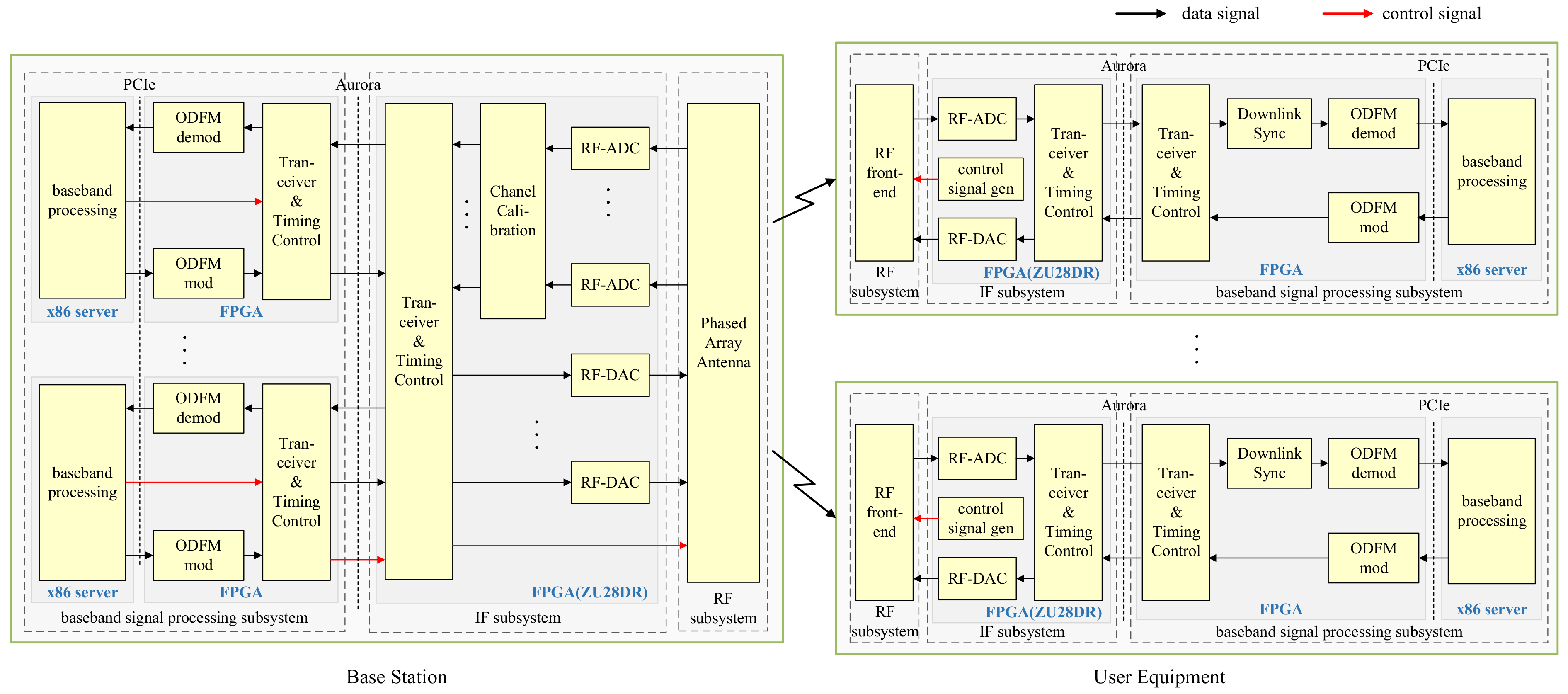
2.1. Hardware Architecture

The testbed is divided into BS part and UE part, and both of them consist of three subsystems: radio frequency (RF) subsystem, intermediate frequency (IF) subsystem and baseband signals processing subsystem, as illustrated in Figure 1. For both the BS and the UEs, the RF subsystem is responsible for the conversion between the IF and RF signal and corresponding RF signal processing, the IF subsystem is responsible for the conversion of the analog IF signal and digital baseband signal as well as the data forward, and the baseband signal processing subsystem is responsible for the processing of the baseband signal. Specifically, the x86 servers are responsible for frequency-domain data processing, while alveo u200 and u50 are responsible for the remaining procedures including OFDM modulation/demodulation and downlink synchronization. Differently, control signals for phased array antenna configuration are generated in the x86 server at the BS side, while the control signals for RF front-end configuration are generated in the ZU28DR at the UE side.
(1) Baseband signal processing subsystem: As for baseband signal processing, the hybrid CPU-FPGA architecture is applied to meet the requirements of high throughput and fast algorithm deployment simultaneously, where the algorithms requiring high throughput and less frequent modifications are deployed on FPGAs, and the remaining algorithms are deployed on x86 servers. To prevent the x86 server from a bottleneck of the testbed’s throughput, techniques including multithreaded programming can be adopted, and the memory of servers should be large enough to avoid potential data congestion on the PCIe bus. Thus, the x86 servers that have Xeon Platinum 8375C CPU with 32 cores and 64 GB DDR4 memory are applied in BS and UEs. Since the BS carries out the processing of multiple UEs’ data, the alveo u200 accelerator cards with more resources are applied in the BS, while alveo u50 accelerator cards are applied in the UEs. In this way, the high throughput requirements of the baseband algorithms are met, and the fast deployment of the algorithms is achieved.
(2) IF subsystem: Since the IF subsystem is supposed to fulfill the conversion between baseband and IF signals as well as analog and digital signals, the RFSoC ZCU111 evaluation kit equipped with radio frequency analog-to-digital converters (RF-ADCs) and radio frequency digital-to-analog converters (RF-DACs) is deployed, where RF-ADCs/RF-DACs integrate digital down converters (DDC)/digital up converters (DUC) for the conversion between IF signals and baseband signals. This kit features a Zynq UltraScale+ RFSoC supporting eight 12-bit 4.096 Gsps ADCs across four tiles, eight 14-bit 6.554 Gsps DACs across two tiles and 16 GTY transceivers [17,18], which enables ZCU111 to exchange data with accelerator card through aurora protocol and to connect RF-ADCs/RF-DACs with RF subsystem via SMA cable.
(3) RF subsystem: To support the characteristics of multi-beam, XL-MIMO, mmWave and adaptive beams, the phased array antenna equipped with configurable phase shifters that operate at the mmWave band is adopted in the BS. The phased antenna array consists of Tx/Rx modules, antenna subarrays and a local oscillator (LO) module, as shown in Figure 2. Detailed descriptions are given in the following content.
1.
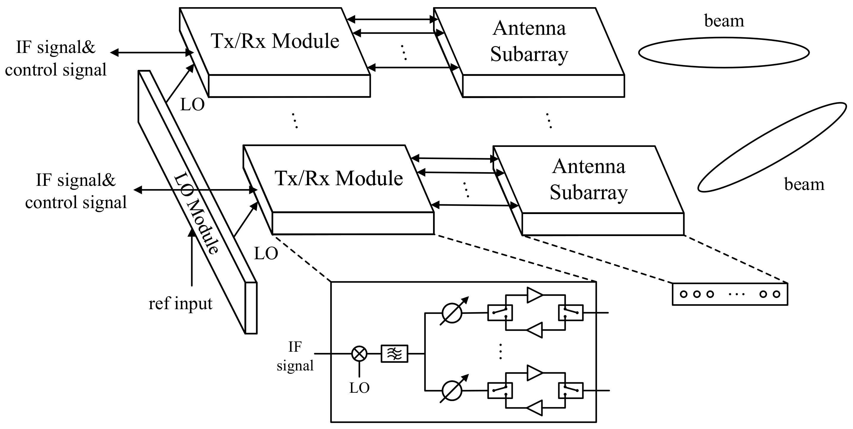
The LO module receives a 10 MHz reference signal and generates a 25.2 GHz LO signal, which is further transmitted to Tx/Rx modules through an power divider for the transmission between 2.8 GHz IF signals and 28 GHz RF signals.
2.
The Tx/Rx module comprises a mixer, a bandpass filter (BPF), a power divider, phase shifters, power amplifiers (PA), low noise amplifiers (LNA) and switches. The Tx/Rx module receives a control signal and configures phase shifters, amplifiers and switches, where the phase shifter is 6-bit quantized with the resolution of 5 . 625 .
3.
As shown in Figure 2, each antenna subarray is equipped with a uniform linear array (ULA) with antennas separated by λ s / 2 , where λ s is the wavelength of the RF signal.
Figure 2. The architecture of the phased antenna array. Phase shifters, amplifiers and switches in Tx/Rx modules are controlled by the control signal, and the control circuit is omitted.
Electronics 12 00380 g002

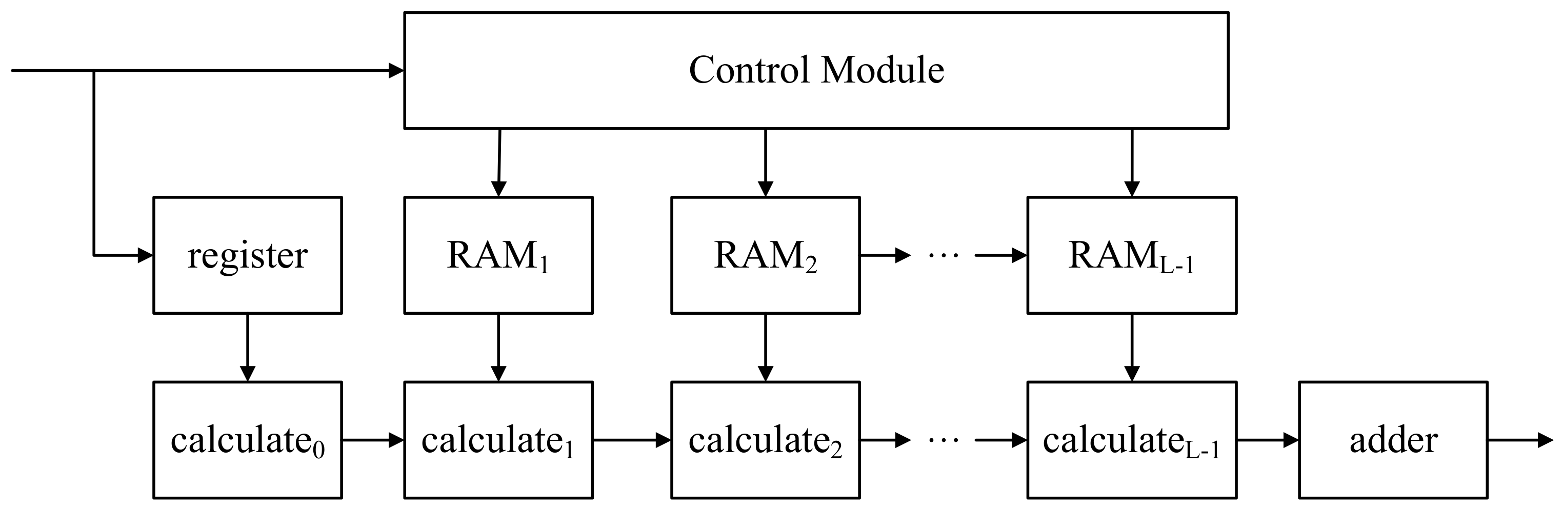
2.2. Channel Calibration

Many array processing algorithms are based on the assumption that there are no phase and amplitude deviations among multiple channels. However, the channel mismatch caused by antennas, amplifiers, ADCs and cables with different lengths at each RF chain will lead to performance degradation of array processing algorithms. To cope with that, channel calibration including phase and amplitude calibration is required. In our testbed, phase and amplitude deviations come from three sources: deviations caused by components inside the phased array antenna including antenna elements and amplifiers, deviations caused by signal propagation in cables of different lengths, and deviations introduced between different ADCs. By calibrating these three parts separately, the channel calibration of the system can be completed.

2.2.1. Calibration of Phased Array Antenna Related Deviation

The phase and amplitude deviations between eight antennas connected to the same RF chain are corrected in this section, since the deviations between RF chains can be compensated along with the cable related deviation.
Consider a ULA of N antennas separated by a distance of λ / 2 , where λ is the signal wavelength. To complete the receiving calibration, a sine wave s ( t ) with frequency f is transmitted via a horn antenna placed in front of the phased array antenna. Ignoring the Gaussian noise, the received signal at the i-th antenna is approximated as
y i ( t ) = h g i r a i r s ( t ) e j 2 π d i / λ e j ϕ i e j ψ i r , i = 1 , 2 , , N ,
where g i r and ϕ i are LNA gain and phase shifter value connected to the i-th antenna respectively, d i is the distance from the horn antenna to the i-th antenna element of phased array antenna, h is the channel gain, a i r and ψ i r are the amplitude and phase errors caused by the active and passive components connected to the i-th antenna. Taking the first antenna as reference, Equation (1) can be rewritten as
y i ( t ) = g i r g 1 r ( t ) γ i r e j 2 π d i d 1 λ e j ( ϕ i ϕ 1 ) e j θ i r · y 1 , i = 1 , 2 , , N ,
where γ i r = a i r / a 1 r , θ i r = ψ i r ψ 1 r . The amplitude and phase differences of the i-th antenna compared to the first antenna can be measured with a vector network analyzer (VNA), denoted as γ i r , V N A and θ i r , V N A , respectively. From Equation (2), we know that
γ i r = g 1 r g i r γ i r , V N A , θ i r = 2 π d i d 1 λ ( ϕ i ϕ 1 ) θ i r , V N A .
Transmitting the sine wave s ( t ) through the i-th antenna at the phased array antenna, the signal x i ( t ) is received at the horn antenna. Similar to the procedure of receiving calibration, the transmitting amplitude and phase deviations denoted as γ i t and θ i t can be expressed as
γ i t = g 1 t g i t γ i t , V N A , θ i t = 2 π d i d 1 λ ( ϕ i ϕ 1 ) θ i t , V N A ,
where γ i t , V N A and θ i t , V N A denote the amplitude and phase differences of x i ( t ) compared to x 1 ( t ) measured with a VNA, g i t , i = 1 , 2 , , N is gain of the PA connected to the i-th antenna. By inserting extra phase shifters and amplifiers with fixed values, the transmitting and receiving calibration are completed, and the Tx/Rx module in Figure 2 can be modified to the architecture in Figure 3.

2.2.2. Calibration of RF-ADC/RF-DAC and Cable-Related Deviation

As mentioned in Section 2.1, the RF-ADCs/RF-DACs are placed across multiple tiles, where each tile has its own independent clocking and data infrastructures. To support multi-beam transmission, more than one tile is required, which needs to synchronize the output of each RF-ADC/RF-DAC with the presence of the clock skew, FIFO latencies and other factors. Fortunately, the multi-tile synchronization (MTS) feature provided by RFSoC ZCU111 can be utilized to achieve relative and deterministic multi-tile alignment.
After the calibration of the RF-ADC/RF-DAC related deviation, the phase errors caused by cables with different lengths need to be corrected, where the cables are used to connect the RF-ADCs/RF-DACs to the phased array antenna. Let β k ( f ) , k = 1 , 2 , 3 , , 8 denote the phase of output signal at channel k (or equivalently, the output of k-th RF-ADC) at frequency f, and φ k ( f ) = β 0 ( f ) β k ( f ) denotes the phase deviation between channel k and channel 0 at frequency f.
In the ideal situation, FIR filters with phase response φ k ( f ) can be adopted to compensate for the phase deviation between channel k and channel 0, thus the output signal phase β ^ k ( f ) of channel k after calibration will be β 0 ( f ) , where the phase deviation between channel k and channel 0 is eliminated. Meanwhile, the amplitude response of the filter for channel k should be close to 1 to keep the amplitude relationship between channel k and channel 0 unchanged after calibration.
To obtain the FIR filters for channel k , k = 1 , 2 , , 7 , we need to obtain the analytic form of the phase deviation between channel k and channel 0. Assume the phase deviation between channel k and channel 0 has the following form:
ψ k ( f ) = p k , 1 f n + p k , 2 f n 1 + + p k , n f + p k , n + 1 ,
where p k , i , i = 1 , 2 , , n + 1 are fit parameters and f is the frequency. By obtaining M samples of frequency f, i.e., f 1 , f 2 , , f M and corresponding measured average phase deviation φ ¯ k ( f 1 ) , φ ¯ k ( f 1 ) , , φ ¯ k ( f M ) , we can rewrite Equation (5) as
f 1 n f 1 n 1 1 f 2 n f 2 n 1 1 f M n f M n 1 1 p k , 1 p k , 2 p k , n + 1 = φ ¯ k ( f 1 ) φ ¯ k ( f 2 ) φ ¯ k ( f M ) .
Solving the above equation, we can obtain the polynomial coefficients p k , 1 , , p k , n + 1 of the polynomial for channel k. After acquiring the analytic form of phase deviations, we will derivate the frequency response of each FIR filter. Let H k ( f ) denote the frequency response of the FIR filter applied for channel k and H k ( f ) can be obtained by minimizing the following Chebyshev norm:
H k ( f ) = arg min H k ( f ) E k ( f ) c h e b ,
where E k ( f ) c h e b is defined as
E k ( f ) c h e b = max f | H k ( f ) exp ψ k ( f ) | ,
where | · | is the absolute value.
It is known that the relationship between the i-th sampling point of an FIR filter’s input s ( i ) and the filter’s output r ( i ) is
r ( i ) = l = 0 L 1 h l s ( i l ) ,
where h l is the l-th tap of the filter, L is the number of taps. Noting that complex multiplication can be written as
( a + j b ) ( c + j d ) = ( a c b d ) + ( a d + b c ) j = ( a + b ) c ( c + d ) b + j ( c + d ) b + ( a b ) d ,
we can rewrite Equation (9) as
r ( i ) = l = 0 L 1 h l s ( i l ) = l = 0 L 1 A i , l l = 0 L 1 B i , l + j l = 0 L 1 B i , l + j l = 0 L 1 C i , l ,
where
A i , l = { h l } + { h l } { s ( i l ) } , B i , l = { s ( i l ) } + { s ( i l ) } { h l } , C i , l = { h l } { h l } { s ( i l ) } ,
where { · } and { · } denote the real part and imaginary part of ( · ) , respectively.
The architecture of the channel calibration module is illustrated in Figure 4. The control module and RAM j collaborate to control the delay of each tap. The calculation module, named calculate j , is responsible for the calculation of l = 0 j A i , l , l = 0 j B i , l , l = 0 j C i , l according to Equation (11) and is implemented using three DSPs. After that, r ( i ) is calculated by adder using the output of calculate L 1 with two DSPs.
The results of seven channel calibration modules are presented in Figure 5 and Figure 6. It can be observed from the figure that the modules can reduce the phase differences from about 40 30 to less than ± 10 , the maximum amplitude deviations are reduced from about −53 dB to less than −55 dB, which meets the requirement of our system.

2.3. Software Architecture

There are also some challenges corresponding to the high-speed process of broadband signals faced by the current architecture. x86 servers might be the bottleneck of the testbed’s throughput because of its disadvantages in high-speed data processing, which means multi-threaded programming, single instruction multiple data (SIMD) and other techniques can be applied for x86 servers processing speed improvement. The detailed solutions to the challenge are presented in the following content.
Figure 7 illustrates the block diagram of the software implementation, including the data storage format of the reception queue and transmission queue and the relationship between different modules. Data stored in the reception queue can be written to disk for data collection, which is omitted in Figure 7.
In the downlink slots, six threads are allocated to the downlink baseband processing module to obtain frequency-domain symbols, which are further written to the transmission queue. Meanwhile, the control signals containing beamforming (BF) vectors for reception and PA gain are generated in the BF vector generation module with one thread and written to the transmission queue. After that, the PCIe transmitter allocated with two threads fetches packets from the transmission queue and sends them to the FPGAs.
In the uplink slots, the PCIe reads data packets from FPGAs to the reception queue, with which two threads are allocated. After that, the uplink data is conveyed to the uplink baseband processing module for bit stream recovery, where 18 threads are allocated. Meanwhile, the BF vector generation module determines users’ positions using uplink data and generates corresponding BF vectors for transmission, which is further written to the transmission queue along with padding data. Finally, the data packets in the transmission queue are sent to FPGAs via the PCIe transmitter.

3. Example: A Multi-Beam mmWave Testbed

Taking the 3rd Generation Partnership Project (3GPP) 5G new radio (NR) standards as a reference, we implemented an example testbed, which uses orthogonal frequency division multiplexing (OFDM) waveform, 5G-like frame structure and system parameters. The system parameters and frame structure design are presented, followed by the description of OFDM modulation/demodulation modules.

3.1. System Parameters Design

The parameters adopted in our testbed are according to 3GPP 5G NR standards [19,20,21]. To obtain high throughput, the subcarrier spacing is designed to be 120 kHz. The IFFT/FFT size of OFDM modulation/demodulation is 4096, while the subcarriers used for transmission and protection are 3168 and 928, respectively. The CP length of the l-th symbol and numerology μ is
N CP , l μ = 144 κ · 2 μ + 16 κ l = 0 or l = 7 · 2 μ 144 κ · 2 μ l 0 and l 7 · 2 μ ,
where κ = T s / T c , T c is the sampling period of the OFDM signals, T s = 1 / ( Δ f r e f N f , r e f ) , Δ f r e f = 15 kHz, N f , r e f = 2048 . According to Equation (13), the CP length is 544 for the first symbol of each subframe and 288 for the rest symbols. The detailed system parameters are summarized in Table 1.

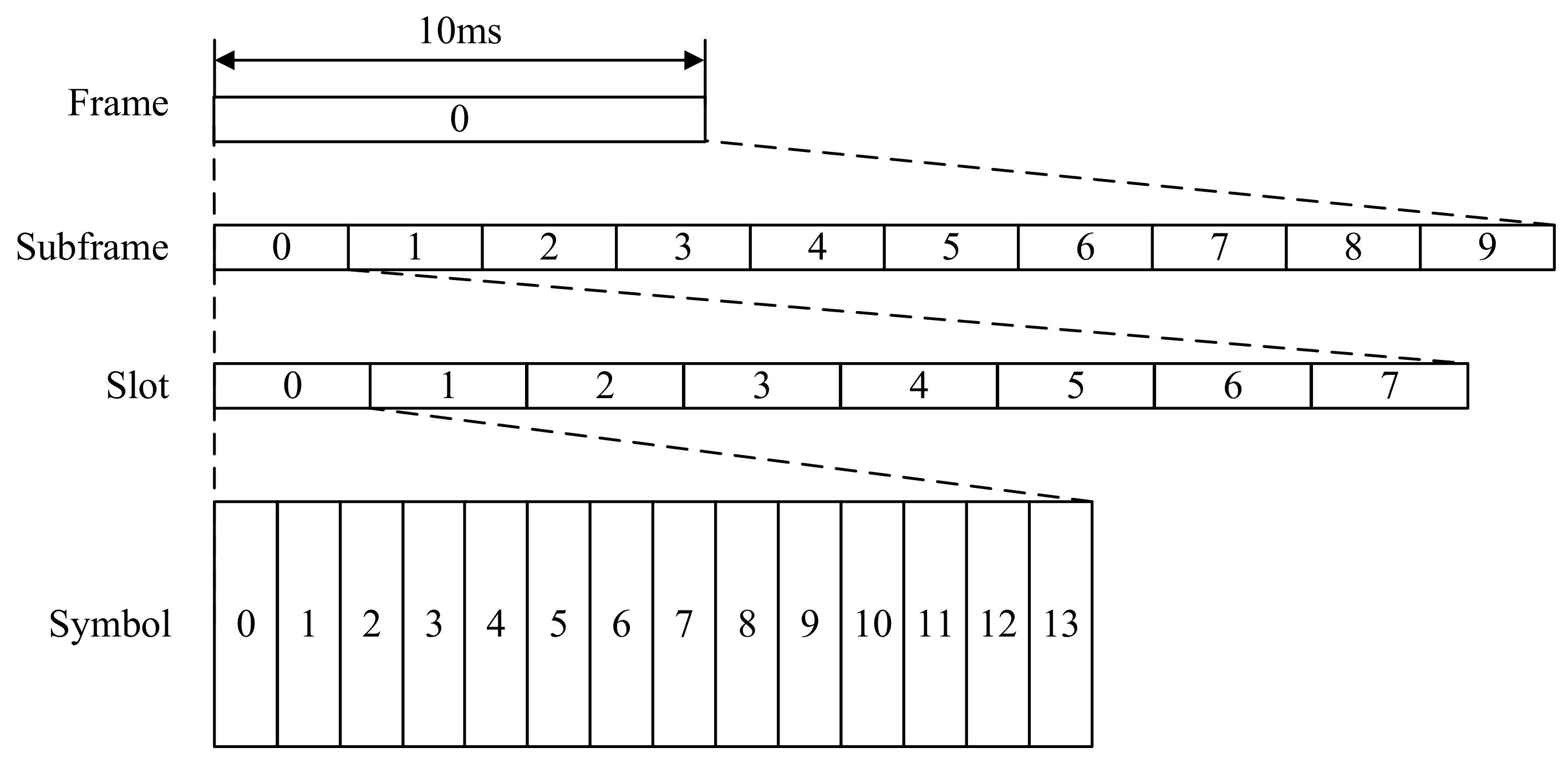
3.2. System Frame Structure

The 5G-like frame structure is adopted in our testbed. Each radio frame has a duration of 10 ms and is divided into ten equal-size subframes of 1 ms duration. Each subframe comprises eight slots for 120 kHz subcarrier spacing. Therefore, each frame consists of 80 slots when subcarrier spacing is 120 kHz. Each slot is further divided into 14 OFDM symbols in our system. The primary synchronization signal (PSS) for downlink synchronization is placed in the first OFDM symbol of each frame according to 5G NR standards. The frame structure designed for our testbed is shown in Figure 8.
In each frame with 80 slots, downlink transmissions are organized in slots 0 to 63, while uplink transmissions are organized in slots 66 to 77. The phased array antenna configuration is organized in the remaining slots. The UEs perform reception and synchronization after power-up. Thereafter, UEs will perform transmission in the coming uplink slots, and the BS will perform reception in pre-allocated uplink slots regardless of UEs’ synchronization state.

3.3. OFDM Modulation and Demodulation

Since FPGA has a maximum clock frequency of hundreds of megahertz while the signal sampling rate is up to 491.52 Msps, the clock frequency of the FPGA is not high enough for the real-time computation of 4096-point IFFT/FFT, a parallel approach of 4096-point IFFT/FFT operation is proposed. Taking IFFT as an example, the input frequency-domain data are divided into four groups with index k 1 and k 2 , each group has N 2 = N / 4 points, where N is the IFFT size. Let k = 4 k 1 + k 2 denote the index of frequency-domain data, k 1 = 0 , 1 , , N 2 1 , k 2 = 0 , 1 , 2 , 3 . Similarly, let n 1 and n 2 denote the index of output parallel data, and n = n 2 N 2 + n 1 is the index of the time-domain data, n 1 = 0 , 1 , , N 2 1 , n 2 = 0 , , 3 . The following equation holds according to the periodicity of the twiddle factor W N n k ,
W N n k = e j 2 π k n N = e j 2 π 4 k 1 + k 2 n 2 N 2 + n 1 4 N 2 = e j 2 π k 1 n 2 + 2 π k 2 n 2 4 + 2 π k 1 n 1 N 2 + 2 π k 2 n 1 4 N 2 = W 4 n 2 k 2 W N 2 n 1 k 1 W N n 1 k 2 .
Let N C P denote the CP length, x ( n ) denote the time-domain sequence obtained by the IFFT operation. By inserting CP into x ( n ) , we can obtain x ( n ) as
x ( n ) = x n 2 N 2 + n 1 = 1 N k = 0 N 1 X ( k ) W N k n W N k N C P = 1 4 k 2 = 0 3 1 N 2 k 1 = 0 N 2 1 X 4 k 1 + k 2 W N 2 k 1 n 1 N C P W N n 1 N C P k 2 W 4 n 2 k 2 .
According to Equation (15), the following steps can be taken to obtain the sequence x ( n ) .
1.
Perform IFFT operation to each 1024-point data channel and then insert N C P -point CP;
2.
Multiply the output of step 1 by the complex number W N n 1 N C P ;
3.
Perform 4-point IFFT to the output of four channels. The first 4096 points of the result sequence are x ( n ) .
The architecture of the corresponding parallel IFFT module is presented in Figure 9. Complex multiplication and 1024-point IFFT are implemented using the CORDIC IP core and FFT IP core, respectively. The 4-point IFFT is implemented simply by adding/subtracting and exchanging real and imaginary parts of data. The results are finally output serially via FIFO.
Similar to the parallel IFFT operation, we can obtain the parallel FFT algorithm. The results can be computed as
X ( k ) = n 2 = 0 3 n 1 = 0 N 2 1 x ( 4 n 1 + n 2 ) W N 2 n 1 k 2 W N k 2 ( n 2 m ) W 4 ( n 1 m ) k 1 .
The hardware architecture of parallel FFT modules is similar to that of parallel IFFT modules and is omitted for simplicity.

4. Experimental Results

In this section, some experiments are carried out to evaluate the performance of our testbed described in Section 3 in the indoor near-field scenario, including the data transmission capability and beam management procedure.

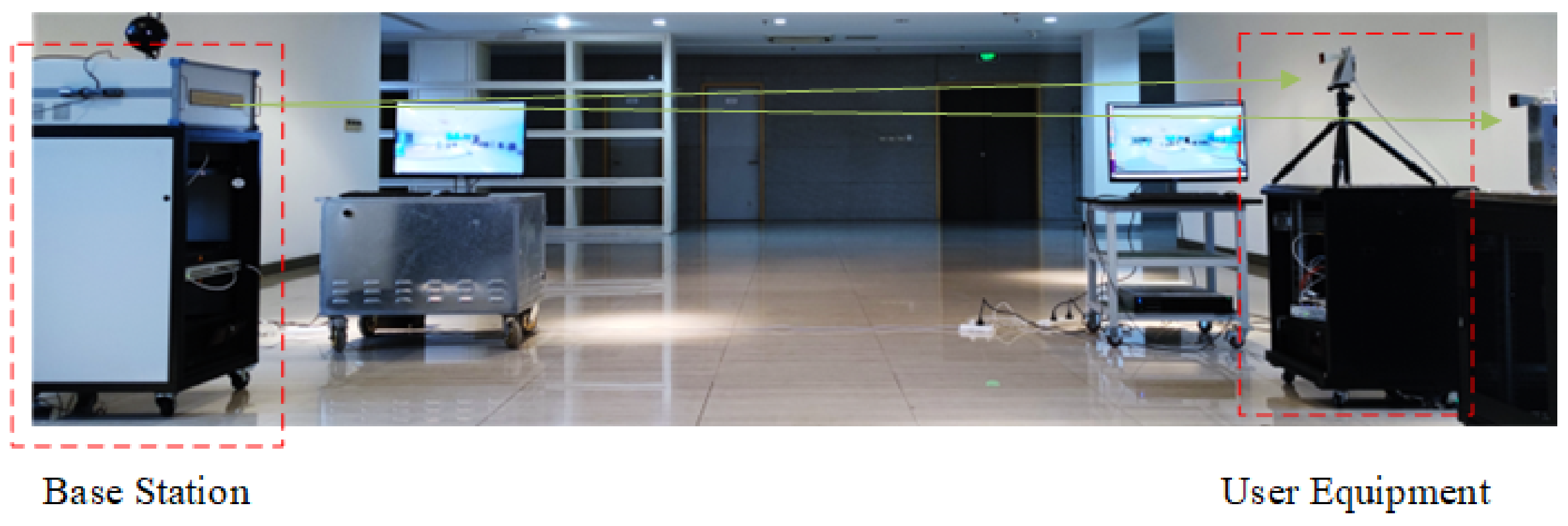
4.1. Measurement Scenario

To verify the performance of our testbed in a multi-beam scenario, two UEs and one BS are used for measurement. They are placed in the indoor near-field scenario, as shown in Figure 10. The first user is placed at an angle of 16 , while the other user is at an angle of −11 , where the positive angle means clockwise to the normal of the BS.

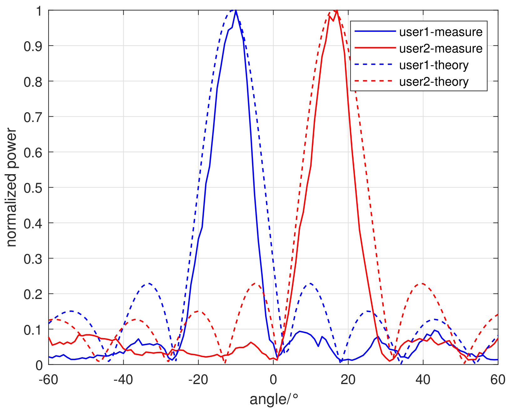
4.2. Beam Management Measurement

As horn antennas are used in UEs, it is required to keep them pointing to the phased array antenna during the movement. The experimental beam patterns and theoretical beam patterns calculated by the UEs’ position are shown in Figure 11. As can be observed from the figure, the received power reaches its peak value at −11 and 17 , respectively, which indicates that the user positions measured by the testbed are −11 and 17 . Considering that the actual positions of the two users are 16 and 11 , the measured angle has an error of about 1 with the actual results, which shows that the measured user positions are in good agreement with the actual positions in the near-field scenario. The same test was performed during users’ movement, and the angle errors are less than ± 1 .

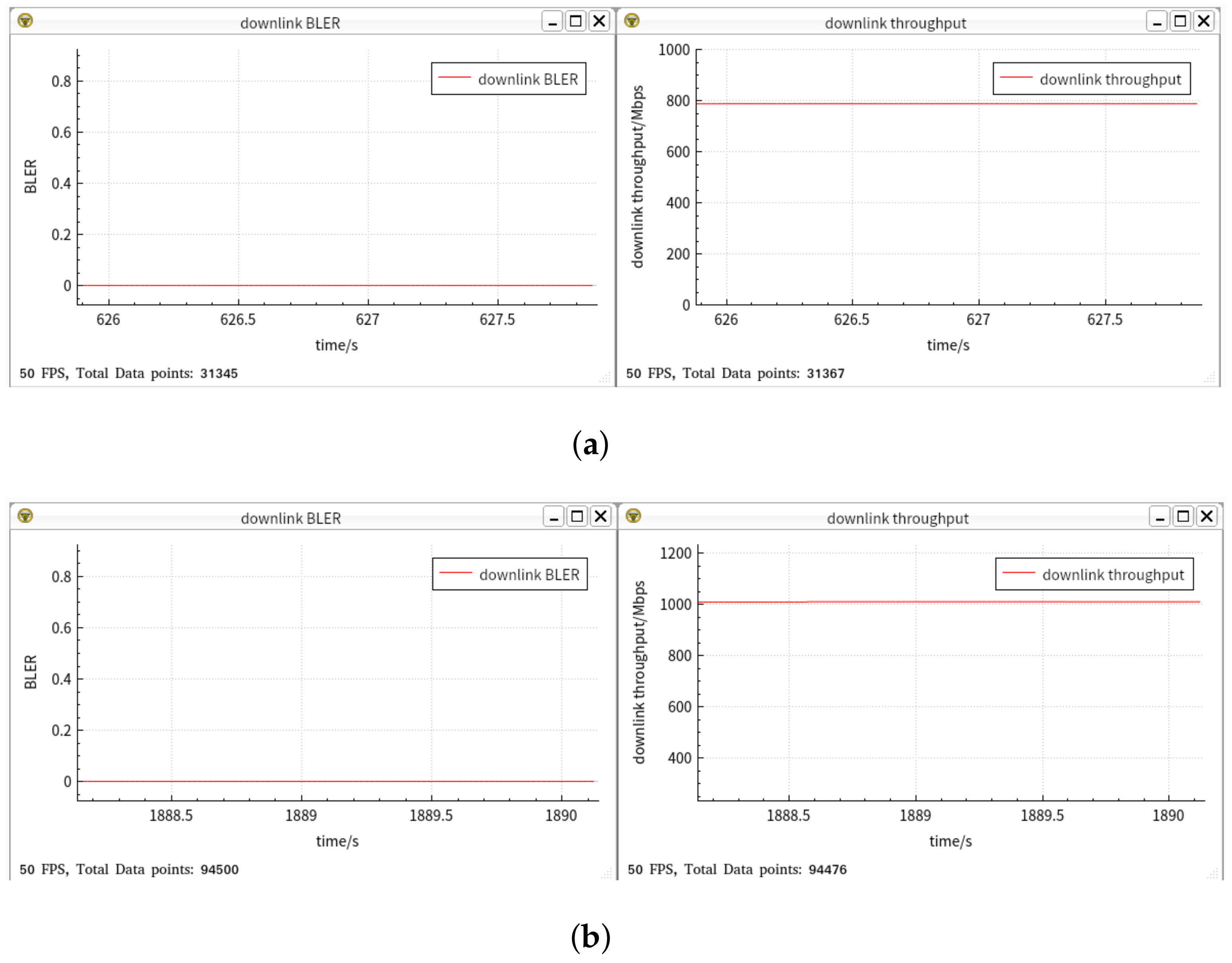
4.3. Data Transmission Measurement

Two modulation schemes, 16-QAM modulation with code rate 658/1024 and 64-QAM modulation with code rate 567/1024, are tested successively with the received IF signal power fixed to −7.5 dBm. When the optimal beam is decided, the BS transmits downlink signals to two users simultaneously and suppresses the interference of sidelobes to the other user. After receiving downlink signals, UEs perform downlink synchronization for frame head determination and OFDM demodulation to obtain frequency-domain symbols at the accelerator card. Thereafter, channel estimation, equalization and other operations are executed on the x86 server, and bit streams are recovered. As can be observed from Figure 12, which presents the constellation after channel equalization, the constellation points of 16-QAM modulation are clear, and the constellation points of 64-QAM modulation are also relatively clear.
The block error rate (BLER) and throughput results of our example testbed are presented in Figure 13. Under the −7.5 dBm received power, the BLER of the two modulation schemes is low (less than 1 × 10 4 during the experiment under both modulation schemes), which means that both modulation schemes can be applied in practical scenarios. In addition, the receiving throughput under 16-QAM modulation and 64-QAM can reach about 787.3 Mbps and 1009.3 Mbps, respectively, indicating that the system can achieve a throughput of more than 1 Gbps of each beam in the near-field scenario.

5. Conclusions

In this paper, we designed and implemented a multi-beam XL-MIMO testbed. Specifically, the flexible and fast deployment of high throughput baseband algorithms is supported in the baseband signals processing subsystem. In the RF subsystem, the value of each phase shifter can be configured as adaptive beam patterns. Moreover, the testbed supports multi-beam transmission after channel calibration. These characteristics make our testbed flexible and high-throughput. The experiment results evaluated in the indoor near-field multi-beam scenarios demonstrated that the angle deviation caused by our beam management module is less than ± 1 and the transmission BLER is close to zero, which verified the excellent performance of our testbed in the near-field scenario.

Author Contributions

Investigation, T.F.; Resources, W.W.; Software, T.F., Y.G., C.S., P.C. and W.X.; Supervision, W.W.; Writing—original draft, T.F.; Writing—review and editing, G.S. and W.W. All authors have read and agreed to the published version of the manuscript.

Funding

This work was supported in part by the National Key Research and Development Program of China under Grant 2019YFB1803102 and in part by the Jiangsu Province Basic Research Project under Grant BK20192002.

Data Availability Statement

Not applicable.

Conflicts of Interest

The authors declare no conflict of interest.

References

  1. Lu, Y.; Dai, L. Double-Side Near-Field Channel Estimation for Extremely Large-Scale MIMO System. arXiv 2022, arXiv:2205.03615. [Google Scholar]
  2. Yang, J.; Zeng, Y.; Jin, S.; Wen, C.K.; Xu, P. Communication and Localization With Extremely Large Lens Antenna Array. IEEE Trans. Wirel. Commun. 2021, 20, 3031–3048. [Google Scholar] [CrossRef]
  3. Wang, Z.; Zhang, J.; Du, H.; Sha, W.E.; Ai, B.; Niyato, D.; Debbah, M. Extremely Large-Scale MIMO: Fundamentals, Challenges, Solutions, and Future Directions. arXiv 2022, arXiv:2209.12131. [Google Scholar]
  4. Giordani, M.; Mezzavilla, M.; Zorzi, M. Initial Access in 5G mmWave Cellular Networks. IEEE Commun. Mag. 2016, 54, 40–47. [Google Scholar] [CrossRef] [Green Version]
  5. Liu, D.; Wang, L.; Chen, Y.; Elkashlan, M.; Wong, K.K.; Schober, R.; Hanzo, L. User Association in 5G Networks: A Survey and an Outlook. IEEE Commun. Surv. Tutor. 2015, 18, 1018–1044. [Google Scholar] [CrossRef] [Green Version]
  6. Polese, M.; Giordani, M.; Mezzavilla, M.; Rangan, S.; Zorzi, M. Improved Handover Through Dual Connectivity in 5G mmWave Mobile Networks. IEEE J. Sel. Areas Commun. 2017, 35, 2069–2084. [Google Scholar] [CrossRef]
  7. Quadri, A.; Zeng, H.; Hou, Y.T. A Real-Time mmWave Communication Testbed with Phase Noise Cancellation. In Proceedings of the IEEE INFOCOM 2019—IEEE Conference on Computer Communications Workshops (INFOCOM WKSHPS), Paris, France, 29 April–2 May 2019. [Google Scholar]
  8. Kuhne, T.; Caire, G. An Analog Module for Hybrid Massive MIMO Testbeds Demonstrating Beam Alignment Algorithms. In Proceedings of the ITG Workshop on Smart Antennas, Bochum, Germany, 14–16 March 2018. [Google Scholar]
  9. Shepard, C.; Yu, H.; Anand, N.; Li, E.; Marzetta, T.; Yang, R.; Zhong, L. Argos: Practical many-antenna base stations. In Proceedings of the 18th Annual International Conference on Mobile Computing and Networking, Istanbul, Turkey, 22–26 August 2012. [Google Scholar]
  10. Shepard, C.; Yu, H.; Zhong, L. ArgosV2: A flexible many-antenna research platform. In Proceedings of the 19th Annual International Conference on Mobile Computing and Networking, Snowbird, UT, USA, 16–20 October 2017. [Google Scholar]
  11. Shepard, C.W.; Doost-Mohammady, R.; Guerra, R.E.; Zhong, L. ArgosV3: An Efficient Many-Antenna Platform. In Proceedings of the 23rd Annual International Conference on Mobile Computing and Networking, Bochum, Germany, 14–16 March 2018. [Google Scholar]
  12. Chung, M.; Liu, L.; Johansson, A.; Nilsson, M.; Zander, O.; Ying, Z.; Tufvesson, F.; Edfors, O. Millimeter-Wave Massive MIMO Testbed with Hybrid Beamforming. In Proceedings of the Asilomar Conference on Signals, Systems, and Computers, Pacific Grove, CA, USA, 1–4 November 2020. [Google Scholar]
  13. Gunnarsson, S.; Chung, M.; Johansson, A.; Liu, L.; Tufvesson, F.; Edfors, O.; Zander, O.; Ying, Z.; Samanta, K.; Clifton, C. mmWave Massive MIMO in Real Propagation Environment: Performance Evaluation Using LuMaMi28GHz. In Proceedings of the Asilomar Conference on Signals, Systems, and Computers, Pacific Grove, CA, USA, 31 October–3 November 2021. [Google Scholar]
  14. Chung, M.; Liu, L.; Johansson, A.; Liu, L.; Tufvesson, F.; Edfors, O.; Zander, O.; Ying, Z.; Samanta, K.; Clifton, C. LuMaMi28: Real-Time Millimeter-Wave Massive MIMO Systems with Antenna Selection. arXiv 2021, arXiv:2109.03273. [Google Scholar]
  15. Wang, K.; Yang, X.; Li, X.; Went, C.K.; Jin, S. SDR Implementation of an End-to-End mmWave Testbed Based on Phased Antenna Array. In Proceedings of the 2019 11th International Conference on Wireless Communications and Signal Processing (WCSP), Xi’an, China, 23–25 October 2019. [Google Scholar]
  16. Yang, X.; Zhang, J.; Yang, B.; Wang, K.; Li, X.; Jin, S. A Scalable Implementation for Real-Time Phased Antenna Array mmWave Testbeds. In Proceedings of the 2019 IEEE/CIC International Conference on Communications in China (ICCC), Changchun, China, 11–13 August 2019. [Google Scholar]
  17. ZCU111 Evaluation Board User Guide (UG1271). Available online: Https://docs.xilinx.com/v/u/en-US/ug1271-zcu111-eval-bd (accessed on 2 October 2018).
  18. Zynq UltraScale+ RFSoC Product Data Sheet: Overview (DS889). Available online: Https://docs.xilinx.com/v/u/en-US/ds889-zynq-usp-rfsoc-overview (accessed on 8 April 2021).
  19. Technical Specification Group Radio Access Network, NR, Physical Channels and Modulation, document 3GPP TS 38.211 V15.9.0, 3rd Generation Partnership Project. June 2021.
  20. Technical Specification Group Radio Access Network, NR, User Equipment (UE) radio transmission and reception, Part 2: Range 2 Standalone, document 3GPP TS 38.101-2 V17.4.0, 3rd Generation Partnership Project. December 2021.
  21. Technical Specification Group Radio Access Network, NR, Base Station (BS) radio transmission and reception, document 3GPP TS 38.104 V16.3.0, 3rd Generation Partnership Project. March 2020.
Figure 1. Overview of our proposed XL-MIMO testbed in the multi-UE scenario.
Electronics 12 00380 g001
Figure 3. Modified Tx/Rx Module for transmitting and receiving calibration.
Electronics 12 00380 g003
Figure 4. The architecture of channel calibration modules.
Electronics 12 00380 g004
Figure 5. Phase deviations of each channel. The phase differences are reduced from about 40 30 to about 10 4 . (a) Phase deviations before calibration; (b) Phase deviations after calibration.
Electronics 12 00380 g005
Figure 6. Amplitude deviations of each channel. The maximum amplitude deviations are reduced from about −53 dB to less than −55 dB. (a) Amplitude deviations before calibration; (b) Amplitude deviations after calibration.
Electronics 12 00380 g006
Figure 7. Data storage format and relationship between different modules.
Electronics 12 00380 g007
Figure 8. The frame structure. Each frame is divided into 80 slots. Each slot is further divided into 14 OFDM symbols.
Electronics 12 00380 g008
Figure 9. The architecture of parallel IFFT module.
Electronics 12 00380 g009
Figure 10. The indoor test scenario.
Electronics 12 00380 g010
Figure 11. The measured and theoretical beam patterns of the given two users scenario.
Electronics 12 00380 g011
Figure 12. Received constellations under different modulation schemes. (a) Received constellation under 16-QAM modulation; (b) Received constellation under 64-QAM modulation.
Electronics 12 00380 g012
Figure 13. The BLER and throughput results of our example testbed. (a) The BLER and throughput results under 16-QAM modulation; (b) The BLER and throughput results under 64-QAM modulation.
Electronics 12 00380 g013
Table 1. System parameters design.
ParamterValue
Carrier frequency28 GHz
Intermediate frequency2.8 GHz
Bandwidth400 MHz
Subcarrier spacing120 kHz
Operation modeTDD
FFT size4096
# of used subcarriers3168
CP length288 or 544
# of OFDM symbols per frame1120
Modulation schemesQPSK, 16QAM, 64QAM
Disclaimer/Publisher’s Note: The statements, opinions and data contained in all publications are solely those of the individual author(s) and contributor(s) and not of MDPI and/or the editor(s). MDPI and/or the editor(s) disclaim responsibility for any injury to people or property resulting from any ideas, methods, instructions or products referred to in the content.

