
Application of Metal Oxide Memristor Models in Logic Gates


Department Fundamentals of Electrical Engineering, Technical University of Sofia, 8 Kliment Ohridski Blvd, 1000 Sofia, Bulgaria
Electronics 2023, 12(2), 381; https://doi.org/10.3390/electronics12020381
Submission received: 2 December 2022
/
Revised: 31 December 2022
/
Accepted: 8 January 2023
/
Published: 11 January 2023
(This article belongs to the Section Artificial Intelligence Circuits and Systems (AICAS))
Abstract
:Memristors, as new electronic elements, have been under rigorous study in recent years, owing to their good memory and switching properties, low power consumption, nano-dimensions and a good compatibility to present integrated circuits, related to their promising applications in electronic circuits and chips. The main purpose of this paper is the application and analysis of the operations of metal–oxide memristors in logic gates and complex schemes, using several standard and modified memristor models and a comparison between their behavior in LTSPICE at a hard-switching, paying attention to their fast operation and switching properties. Several basic logic gates—OR, AND, NOR, NAND, XOR, based on memristors and CMOS transistors are considered. The logic schemes based on memristors are applicable in electronic circuits with artificial intelligence. They are analyzed in LTSPICE for pulse signals and a hard-switching functioning of the memristors. The analyses confirm the proper, fast operation and good switching properties of the considered modified memristor models in logical circuits, compared to several standard models. The modified models are compared to several classical models, according to some significant criteria such as operating frequency, simulation time, accuracy, complexity and switching properties. Based on the basic memristor logic gates, a more complex logic scheme is analyzed.
Keywords:
metal–oxide memristor models; modified window function; OR; AND; NOR; NAND; XOR; LTSPICE library models; logic gates1. Introduction
The memristor element, predicted by Chua in 1971 and formed in 2008 by Stanley Williams, is a nano-size, passive, two-terminal and highly nonlinear electronic element with good switching and memory properties [1,2]. The first material memristor prototype was built on amorphous titanium dioxide (TiO2), incompletely saturated by oxygen vacancies. It could hold its conductance after switching the sources off. Its resistance is altered by external current or voltage pulses [2,3]. Together with the various types of memristors, such as polymeric, magnetic tunnel, spintronic and others, the memristors founded on transition metal oxides are preferably analyzed, due to their better memory and switching properties, stable parameters and characteristics [2]. Memristors are applicable to many different electronic circuits and devices, such as neural networks, non-volatile memories, digital and analog reconfigurable circuits, logical gates, in-memory computing schemes and many others [4,5,6,7]. The manufacturing of such electronic schemes requires accurate and high-speed functioning SPICE (Simulation Program with Integrated Circuits Emphasis) [8] memristor models, and this is the main reason that several of the standard metal–oxide memristor models, such as those of Biolek [9,10] and Lehtonen–Laiho [11], can be improved by modifications and by applying different window functions [6,11,12]. This paper is motivated by the necessity of realization of high-speed logic gates [13,14,15] and more complex digital logical schemes with a large number of memristors in chips [16], which are very important for the realization of electronic circuits with artificial intelligence. They are successfully applicable in the electronics industry and are based on the present Complementary Metal Oxide Semiconductor (CMOS) integrated circuits technologies, where the metal–oxide memristors are effectively used, due to their nano-size dimensions, lower power consumption, the possibility of operation in a hard-switching mode, representing rectifying effects and good switching and memory properties, and a comparison of their basic classical and modified models, according to their behavior and switching properties in the SPICE environment. For the realization of the main logical functions NOT, OR, AND, and more complex logic schemes such as NOR, NAND and XOR, the metal–oxide memristors are used together with CMOS transistors in complete structures. In this work, the LTSPICE (Linear Technology SPICE) software [17,18] is used, because it is an open and free environment, very convenient for electronic circuits simulations and analysis, and is preferred by many research engineers and scientists.
In Section 2, a brief description of metal–oxide memristors and their basic models is presented. Section 3 discusses the realization of metal–oxide memristor models in LTSPICE. Section 4 represents the considered memristor-based logic gates and circuits and their behavior. A more complex logic scheme, based on the fundamental AND, OR and NOT logical elements is analyzed in the LTSPICE environment in Section 5. In Section 6, a comparison of the considered memristor models, according to several important criteria, is presented. The results are discussed in Section 7. The concluding remarks are presented in Section 8.
2. Metal–Oxide Memristors and Their Modeling
In this section, a brief introduction to metal–oxide memristors and their modeling is presented, for the better understanding of their operation and applicability in logic schemes. Two main types of such memory elements are filament-type and interface-type memristors. Together with their advantages, such as good memory and switching properties, low energy consumption, and nano-size dimensions, the memristors have some disadvantages, according to CMOS elements, such as comparatively low OFF to ON ratio, not very high endurance and other specific effects. However, the memristors have many promising applications in non-volatile memories with very high density, in neural chips and other electronic devices with artificial intelligence. Although the memristors are under intensive investigations and analyses, they are still manufactured in small-size laboratories and the created prototypes of memristor integrated circuits and chips are not applied in mass production at the present moment. However, the manufacturing, modeling and engineering of memristors and memristor-based schemes are key points in the design and generation of novel electronic devices and circuits with optimized performance and various applications.
2.1. Basics of Metal–Oxide Memristors and Their Modeling
The widely applicable and analyzed metal–oxide memristor elements are based on titanium, hafnium, niobium, tantalum and other transition metals [2]. The metal oxide memristor element has two terminals—anode and cathode, sometimes denoted as top electrode (te) and bottom electrode (be) [2,19]. A thin layer of metal oxide partially doped by oxygen vacancies is placed between the electrodes. In the doped region of the oxide material, a certain amount of oxygen vacancies with a positive charge are available. Their quantity is proportional to the resistance of the memristor element, also known as a memristance and usually denoted by M [1]. The memory effect of the memristor element is based on accumulating electric charges, proportional to the time integral of the electric current. The switching properties of the memristor are related to the change of its memristance between a minimal and a maximal value, denoted by RON and ROFF. The state variable of the memristor is usually denoted by x and is expressed as a ratio between the sizes of the doped region and those of the whole memristor. Its change is proportional to the time integral of the applied voltage [1].
Several related standard memristor models, such as those of Williams–Strukov [1], Joglekar [4], Biolek [9] and Lehtonen–Laiho [11] are used and analyzed in the present paper. Some modified and improved metal–oxide memristor models are applied as well [20,21]. Each metal oxide-based memristor model contains at least two or more basic equations. The first one represents the state-dependent relationship between the memristor current I and the applied voltage v [1,6]—Equation (1):
where the conductance of the memristor G(x), also known as a memductance, changes between its OFF-state and ON-state limiting values—GON and GOFF. Their reciprocal values are denoted as RON and ROFF and are known as ON-state and OFF-state memristances. When the OFF and ON resistances of memristors have high values, then the memory element has lower power consumption. The second and the other equations of the metal oxide memristor model, if available, relate the time derivative of the memristor state variables (in the present case—the quantity x) and the current [1,6]—Equation (2):
In Equation (2), k is a physical constant, dependent on the ionic dopant mobility µ, the specific resistance of the memristor element, and its sizes, and f(x) is a window function, ensuring the restriction of the state variable x in the range [0, 1] and representing the boundary effects for a hard-switching operating mode [6,9,16]. The solution of Equations (1) and (2) leads to the deriving of the current–voltage relationship of the memristor, dependent on the initial value of the state variable x0 [6]. In most cases, these equations are numerically solved, using a suitable software environment. In the next sub-section, two standard memristor models (Biolek and Lehtonen–Laiho) and two improved models, denoted by B1 and B2 and based on the Biolek and Joglekar models, are described.
2.2. A description of the Applied Metal–Oxide Memristor Models
In the first part of this sub-section, the classical memristor models of Biolek [9] and Lehtonen–Laiho [11] are discussed.
The memristor model proposed by Biolek [9] is frequently used for analysis of titanium dioxide memristors and memristor-based circuits and is presented by Equation (3). The first equation includes the memristor state variable x and expresses the current–voltage dependence, while the second one presents the relationship between the time derivative of the state variable x and the memristor current i [9]:
According to the first equation, the structure of the memristor could be represented as a series connection of the doped and the un-doped regions. The window function fB(x,i), proposed by Biolek and included in Equation (3) is presented by (4) [9]:
where p is a positive integer, and the expression stp(.) is the standard Heaviside step function [9]. The classical Biolek window is able not only to restrict the state variable x in the interval [0, 1], but also to suitably represent the boundary effects for a hard-switching mode [6,9]. The classical Heaviside function stp(.) is a simple one, but it is a non-differentiable math expression and sometimes leads to convergence problems in the SPICE environment [2,9]. As a complete structure, the Biolek model is a simple and very good one, but it could not completely express the change in the ionic mobility for higher-level signals and usually operates at low- and middle-frequency signals.
The standard Lehtonen–Laiho memristor model [11] is frequently used for analysis of titanium dioxide and hafnium dioxide memristors and is represented by Equation (5). The first equation, relating the memristor current and the voltage, includes two math terms. The first one is an exponential dependence on the voltage, and the second term contains the state variable and a sine–hyperbolic dependence on voltage [11]. The second equation relates the time derivative of the state variable x and the voltage v. The standard Biolek window function fB(x,i) [9] is used in the state differential equation:
The coefficients γ, χ, n, β, α, a and m are used for tuning the memristor model, according to experimental current–voltage characteristics of metal–oxide memristors [6,11]. The Lehtonen–Laiho model is a comparatively complex one, and includes a large number of elementary math operations. It requires a high amount of computer resources for the simulation of devices and circuits with many memristors [6]. This model has very good accuracy, it is flexible, and could successfully express the alteration of the ionic dopant drift mobility with the applied memristor voltage.
In the following second part of this paragraph, two modified memristor models [20,21] are discussed. The first modified metal–oxide memristor model, which will be denoted by B1 [20], is based on the Biolek model and uses a modified window function with an additional sinusoidal component. It is expressed by the next Equation (6).
The first equation of the considered modified memristor model B1 represents the relationship between the current and voltage, and the quantities GOFF and GON are the OFF-state and ON-state conductances of the memristor, connected in parallel. A modified Biolek window function, based on the improved analog of the classical Heaviside step function, uses an enhanced version of the standard Biolek window. The included activation threshold vthr allows the operation of the memristor model in different modes—hard-switching and soft-switching, and also as a linear resistor with a constant value. If the memristor voltage is lower than the activation threshold vthr, then the state variable x remains with its initial value and the memristor behaves as a linear resistor [6,20]. Otherwise, the state variable x changes proportionally to the time integral of the applied voltage. At a hard-switching mode, the state variables reach their boundary values and the memristor behaves as a semiconductor-rectifying diode. In logic gates and schemes, the memristors usually operate in a hard-switching mode and the memristance changes in a very broad interval.
A smooth and differentiable step-like function stpp(.) is expressed by the final equation of the memristor model and is applied instead of the standard Heaviside function. This sigmoidal function is applied for a partial avoidance of convergence problems in the SPICE environment. Its sharpness in the region of switching is controlled by the coefficient s. This modified memristor model has a good accuracy, a little bit lower, but very near to those of the Lehtonen–Laiho model [11]. The modified model [20] is simplified, with a reduced number of the mathematical operations, and due to this it operates faster than the original Lehtonen–Laiho memristor model.
The second modified metal oxide memristor model B2 [21] is based on the standard Joglekar and Biolek models and on a modified window function with an additional polynomial component. It is presented by Equation (7). The first equation of the modified model relates the memristor current i and voltage v:
The state differential equation takes into account the nonlinear ionic dopant drift, dependent on the memristor voltage, and also includes the activation threshold, separating the basic operating modes of the metal oxide memristor. The used modified window function is based on both Biolek and Joglekar windows and has a high nonlinearity. It changes in a broad range and ensures the operation of the model at low-level and high-frequency signals [21]. The considered modified memristor model includes an activation threshold, separating its operation as a linear resistor and as a memory element.
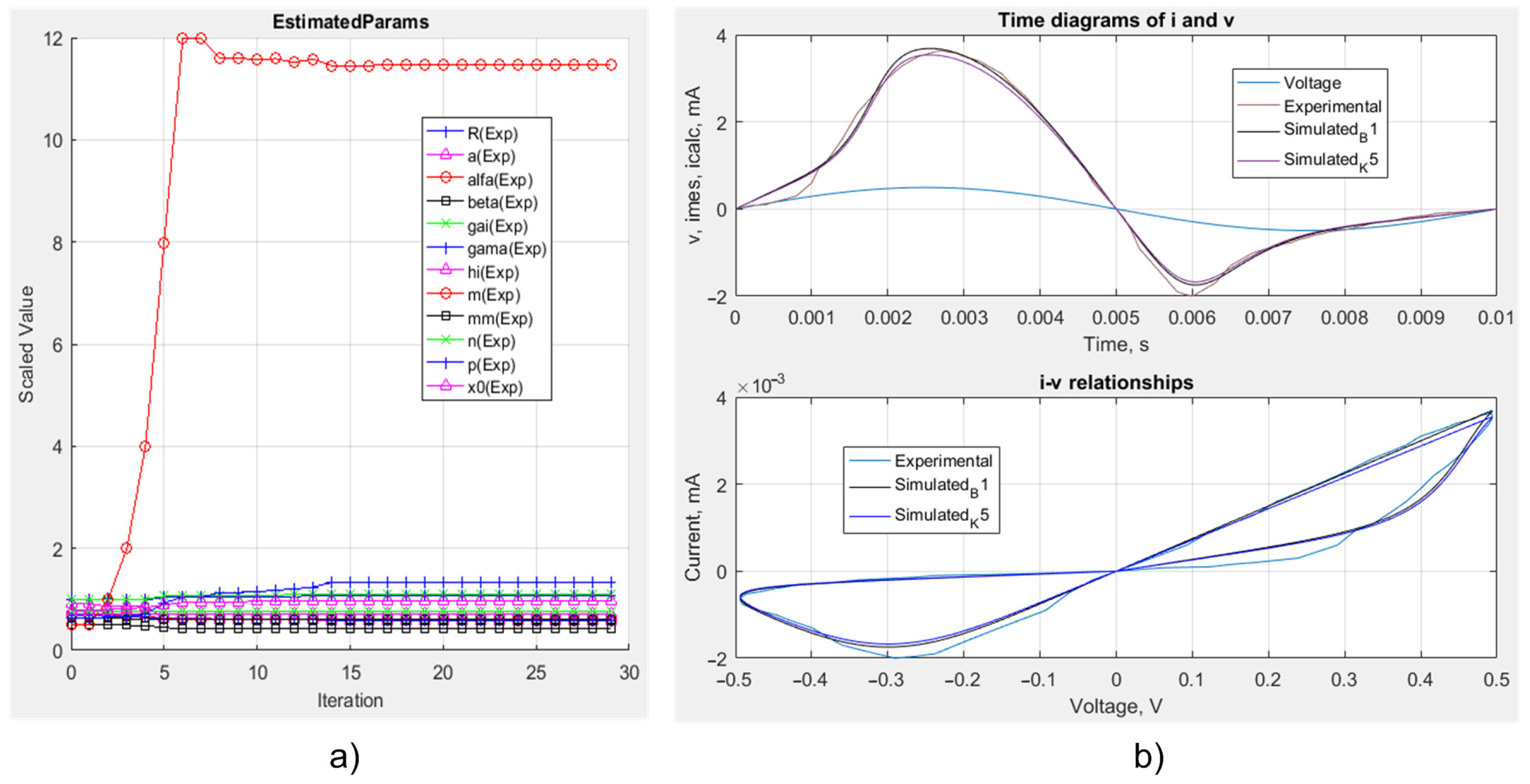
The adjustment of the described memristor models is based on a comparison to the experimental current–voltage relationships of metal–oxide memristors and minimization of the Root Mean Square (RMS) error between them in a Simulink and MATLAB environment. The optimization procedure is based on a gradient descending algorithm [6,11]. The trajectories of the parameters of the Lehtonen–Laiho memristor model are presented in Figure 1a for a representation of the tuning processes of such models. Similar procedures are used for tuning the other considered memristor models. After obtaining the optimal values of the parameters, the memristor models are analyzed in a sinusoidal mode, and the time diagrams and the respective current–voltage characteristics are presented in Figure 1b for comparison of the results. According to the error, the Lehtonen–Laiho model has the minimal RMS error, followed by the models B2, B1 and the Biolek model. Additional experiments at sine-wave signals with different frequencies confirm that all the considered models express shrinking the current–voltage hysteresis loops with increasing the frequency, which is one of the main fingerprints of the memristor elements [1,6].
In the next section, the LTSPICE realization of the described standard and modified metal–oxide memristor models is considered, paying attention to the integration of the time derivative of the memristor state variable and a technique for a partial prevention of convergence problems.
3. LTSPICE Memristor Models’ Realization
Compared to the other SPICE products for analysis and simulations of electronic circuits and devices, such as OrCAD PSpice, HSPICE, CADENCE and others, the LTSPICE software is considered preferable by many researchers and scientists due to its open and free license, the simple and user-friendly interface and improved convergence [8,18]. These are the main reasons for this software to be applied in the present research. LTSPICE software was initially created by Linear Technology and is now developed by the Analog Devices Corporation [8]. This software could be freely downloaded and installed on Windows and Mac operating systems, using the following link: https://www.analog.com/en/design-center/design-tools-and-calculators/ltspice-simulator.html (accessed on 12 October 2022). The LTSPICE environment allows a simplified generation of new and user-defined elements and schematics and their analysis at different operating modes.
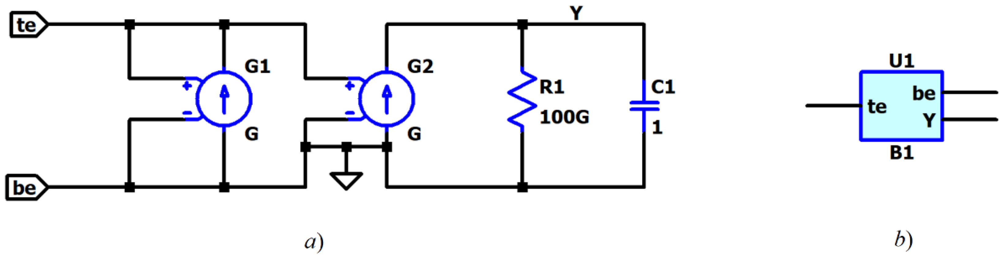
An equivalent LTSPICE schematic of a metal–oxide memristor model is presented in Figure 2a for discussion and explanation of its operation. It is based on the corresponding mathematical models of metal–oxide memristor elements. The main terminals of the memristor are denoted as te (top electrode, anode) and be (bottom electrode, cathode). The terminal Y is an optional one, and its electric potential is proportional to the memristor state variable x [18]. The current of the dependent source G2 represents the time derivative of the memristor state variable, according to the respective state differential equation of the memristor model. This current is integrated by the capacitor C1 to obtain the memristor state variable x. The resistor R1 has a very high resistance and partially prevents the occurrence of convergence problems in the SPICE environment. The transition of the voltage across the capacitor changes more smoothly, when the resistor R1 is connected in parallel to it, and in this way the convergence in SPICE is improved. The dependent source G2 is controlled by the voltage across the memristor, the current of which flows through the source G1. The symbol of the memristor model B1 in LTSPICE environment is presented in Figure 2b for an expression of its visualization in electronic circuits and schemes [12,18].
The applied analyses of memristor models and many other standard and modified models’ LTSPICE codes with detailed explanations for generation and use are freely accessible at the following link: https://github.com/mladenovvaleri/Advanced-Memristor-Modeling-in-LTSpise (accessed on 18 October 2022) [12].
4. Memristor-Based Logic Gates
In this section, several basic and commonly used memristor-based logic gates [22,23,24]—AND, OR, NAND and NOR—are considered and analyzed, applying the previously discussed standard and modified metal–oxide memristor models. An XOR logical scheme with a large number of memristors, based on the main logic gates, is also considered and analyzed, and the successful and fast operation of the modified metal–oxide memristor models is confirmed. Various types of memristors, such as interface-type and filament type, are applicable to logic circuits and schemes [25,26,27,28]. The memory effects of metal–oxide memristors are based on different conductive mechanisms and the accumulation of electric charges in the nanostructure [1,2]. In logic gates and schematics, based on CMOS elements and memristors, a switching mechanism is applied [28]. When the resistances of the switching elements in ON and OFF states have high values, then the power consumption is decreased. In this sense, the engineers and scientists make a lot of effort, together with professionals in different fields of science, such as physics, chemistry and technology, to optimize the manufacturing technology of memristor-CMOS based integrated circuits, paying attention to the development of new materials and techniques for increasing the OFF to ON ratio, for improvement of the switching and memory properties and the endurance of memristor elements.
4.1. Memristor-Based AND Gate
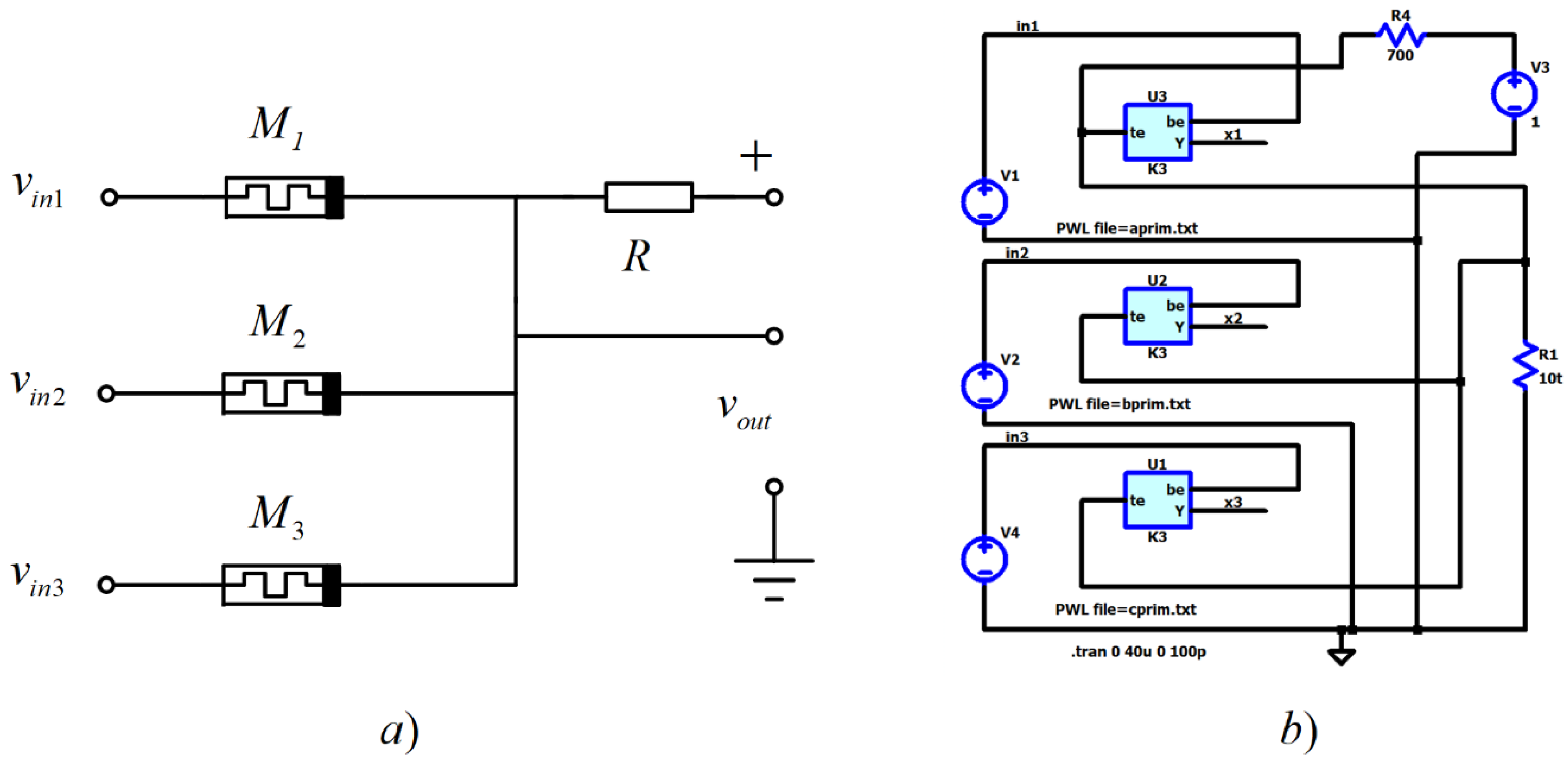
The considered AND logic gate with three inputs is shown in Figure 3a, and its LTSPICE realization in Figure 3b for additional discussion on its structure and principle of operation [23,24]. The schematic is based on the standard diode-resistor logic gate AND [23,24], by replacement of the semiconductor diodes with metal–oxide memristors, denoted by M1, M2 and M3 in the first sub-figure and by U1, U2 and U3 in the LTSPICE schematic presented in Figure 3b. The signal of logical unity is presented by a voltage pulse with a positive polarity and a level of 1 V. The duration of the pulses is about 90 ns. The logical zero is coded by pulses with the same duration and a level of −1 V, due to the necessity of a hard-switching operation of different types of metal–oxide memristor elements—filament and interface-type memristors [25,26,27]. The resistance R is about 700 Ω. If all the input signals are unities, then the memristors are in the OFF state and the output voltage signal corresponds to logical unity. In all other cases, the output voltage signal corresponds to logical zero.
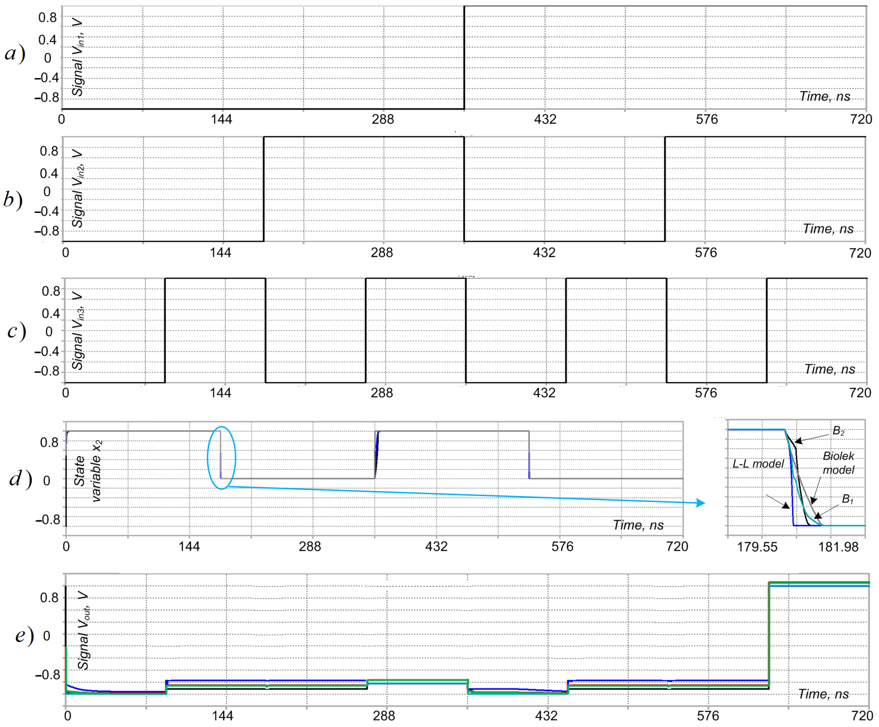
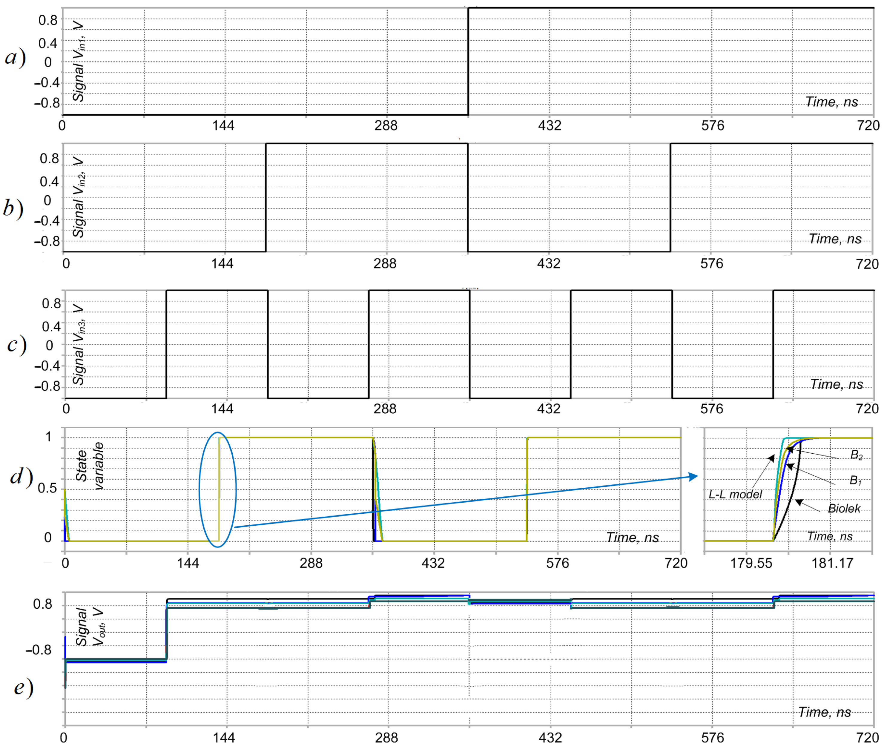
Figure 4a–c represent the time diagrams of the input voltage signals vin1, vin2 and vin3; the respective memristor state variable x2 is shown in Figure 4d and the output signal vout in Figure 4e, according to the behavior of the applied metal oxide memristor models. The memristor state variables according to the used classical and modified models alter between unity and zero, but with different switching times. Observing the change of the memristor state variable in the zoomed time diagram—Figure 4d—it is visible that the Lehtonen–Laiho model corresponds to the lowest switching time, followed by the modified memristor models B1, B2 and the standard Biolek model. The time diagram of the output signal, presented in Figure 4e, confirms the proper operation of the three-input logic gate, realizing the logical function AND.
4.2. Memristor-Based OR Gate
The schematic of a memristor-based OR gate with three inputs is presented in Figure 5a for a description of its structure and functioning [24]. Its LTSPICE realization, needed for analysis and simulations, is shown in Figure 5b. If some of the signals vin1, vin2 or vin3 or all of them are logical unities, then the respective memristors are in ON-state and the output signal has a high value, corresponding to logical unity. Only if all the input signals are zero, will the output voltage have a very low level and correspond to logic zero. The time graphs of the input signals are shown in Figure 6a–c, the state variable x2 is depicted in Figure 6d and the output signal is presented in Figure 6e for further discussion. From the time diagram shown in Figure 6e it is visible that the output signal corresponds to logic function OR.
The state variables of the memristors, according to the applied standard and modified models, varies between zero and unity, owing to the operation of the memristor elements in a hard-switching mode. The considered standard and modified memristor models express different switching times. From the curves presented in the zoomed time diagram in Figure 6d, it is visible that, according to the variation of the state variable, the Lehtonen–Laiho memristor model has the shortest switching time, followed by the modified models B1, B2 and the standard Biolek memristor model.
4.3. Memristor-CMOS Based NAND and NOR Gates
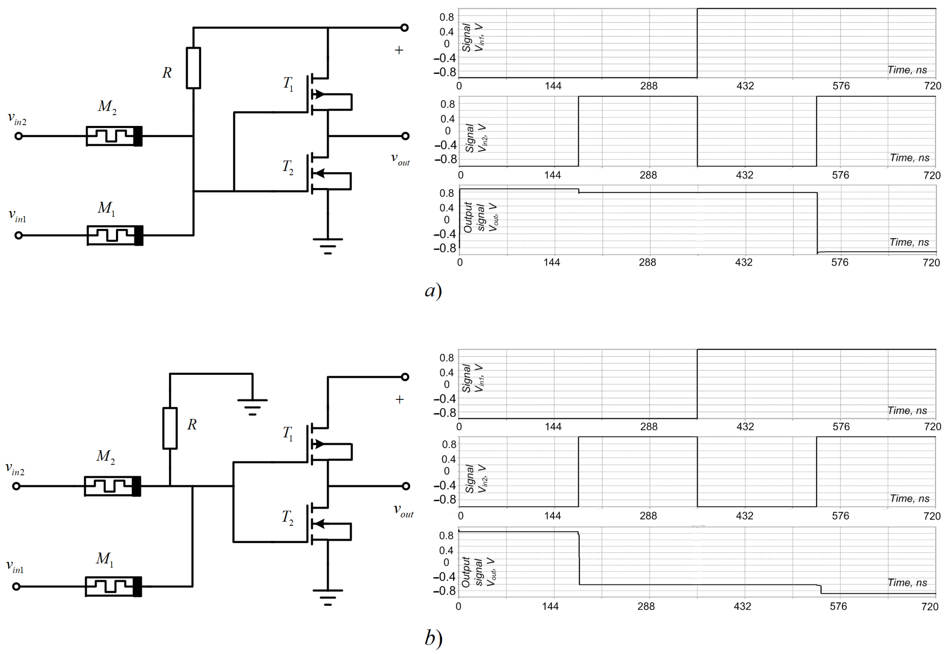
In this paragraph, NAND and NOR logic gates, based on CMOS transistors [22,23] and metal–oxide memristors, are considered and presented in the left-hand side of Figure 7a,b for further description and explanations. In these logic circuits, the memristors are responsible for the realization of logical operations AND, OR, while the CMOS transistors are used for the logic operation NOT. The transistor T1 is an n-channel MOSFET of type Si4866DY, and the element T2 is a p-channel MOS transistor of type IRF7210. The respective time diagrams of the input and output signals are presented in the right-hand-side of Figure 7 for confirmation of the correct operation of the applied memristor models—Biolek, Lehtonen–Laiho, B1 and B2 and the considered logical schematics in the LTSPICE environment.
5. A Complex Memristor-Based Logic Circuit
In this section, a XOR logical scheme based on a large number of memristors and CMOS transistors is considered and shown in Figure 8a for additional explanation and discussion. The input signals of the logical scheme are denoted by vin1 and vin2, and the output signal by vout. The XOR logical function is realized, using the elementary logic operations AND, OR and NOT [23]. The considered schematic is realized using two logic gates NOT, two logic gates AND, and a logical element OR. The first invertor is created by the MOSFET transistors T1 and T2, and the second one by the MOS transistors T3 and T4. The first AND element is created by the memristors M1 and M2, and the second logical element AND by the metal–oxide memristors M4 and M5. The OR logic gate is represented by the memristors M3 and M6.
The time diagrams of the input signals vin1, vin2, and the output signal vout, are represented in Figure 8b for confirmation of the proper operation of the considered complex logic circuit with many memristors and the applied classical and modified metal–oxide memristor models. Considering the time diagram of the output voltage vout, presented in Figure 8d, it is visible that the logical function XOR is successfully realized by the considered CMOS-memristor based logical scheme.
In the next section, a brief comparison of the applied LTSPICE memristor models, according to their behavior, switching properties and several basic criteria, is presented.
6. A Comparison of the Applied Memristor Models
The metal–oxide memristor models, used for analysis of the considered logic circuits, are compared according to their behavior in the analyzed logical circuits and using several main criteria for comparison—simulation time, switching properties, operating frequency, RMS error, accuracy and complexity [6,16]. The results are summarized in Table 1 for comparison of the metal–oxide memristor models.
The simulation time of a memristor model is proportional to the amount included in its equation’s elementary mathematical operations. In the present case, the standard Biolek memristor model has the lowest simulation time and, owing to this, the highest operating speed, followed by the metal–oxide modified memristor models B1 and B2 and the standard Lehtonen–Laiho model.
The complexity of a memristor model is proportional to its simulation time and depends on the number of math operations included in the model. According to the complexity, the modified metal–oxide memristor models B1 and B2 are simpler than the classical Lehtonen–Laiho model, which has the highest complexity. The enhanced models B1 and B2 have high accuracy and operating frequency, very near to those of the Lehtonen–Laiho memristor model. Owing to their reduced complexity, the modified models B1 and B2 are appropriate for the analysis of complex electronic circuits and devices with a large number of memristor elements.
The switching properties of a metal oxide memristor model are related to the rapid change of the memristance and the respective state variable under applied voltage or current pulses. In the present case of consideration, the Lehtonen–Laiho model has the best switching properties, followed by the modified metal–oxide memristor models B2, B1 and the classical Biolek memristor model.
The operating frequency of a memristor model depends on its ability to properly express the change of the state variable and the memristance, proportionally to the applied voltage signals. For metal oxide-based memristor models, low frequency is between 0.5 Hz and 1 kHz; middle frequency between 1 kHz and 100 kHz, respectively; and high frequency no lower than 100 kHz. The Lehtonen–Laiho memristor model has the highest operating frequency, followed by the modified metal–oxide memristor models B2, B1 and the standard Biolek model.
The root mean square (RMS) error of a metal–oxide memristor model is expressed as a sum of the squared differences between the values of the memristor current, according to experimental and simulated current–voltage relationships.
The accuracy of a metal–oxide memristor model is inversely proportional to its RMS error. It represents its capability to correctly express experimental current–voltage relationships with a minimal error. When the RMS error is not higher than 4%, the accuracy of the memristor model is high, the middle accuracy of a memristor model corresponds to an RMS error between 4 and 6%, and the low accuracy is related to an RMS error higher than 6%. The standard Lehtonen–Laiho memristor model has the best accuracy, followed by the improved models B2, B1 and Biolek’s standard memristor model.
7. Discussion
In this work, several memristor-CMOS based logic schemes are considered and analyzed. For the emulation of the logical functions AND, OR, a hard-switching operation of the memristor elements is required. For the realization of the basic logical function NOT, CMOS transistors are applied for inversion of the input signal. The analysis of the considered memristor-CMOS based logic gates AND, OR, NAND, NOR and a more complex digital circuit with many memristors, realizing XOR logic functions in LTSPICE, confirms that the applied modified and improved metal–oxide memristor models, together with the standard Lehtonen–Laiho model have better switching properties than the standard Biolek memristor model. The standard Biolek model and the applied modified memristor models have faster operation in the SPICE environment, owing to their simplified expressions, and they are successfully applicable for analyses of complex digital memristor-CMOS-based logical electronic circuits.
8. Conclusions
After the conducted analyses of several memristor-CMOS based logic gates and more complex digital schemes with many memristor elements, realizing AND, OR, NAND, NOR and XOR logical functions in LTSPICE environment, it could be concluded that the applied modified and improved metal–oxide memristor models, together with the standard Lehtonen–Laiho model, have better switching properties and a little bit lower operating speed than the classical Biolek model and are effectively applicable in complex logical electronic schemes. When applied in the memristor models’ smooth and differentiable step-like function, the modified window functions, based on the improved sigmoidal function and the use of LTSPICE environment, prevent the occurrence of convergence problems during the simulations and analyses. The modified memristor models have faster operation than the corresponding standard memristor models and, owing to this, they are suitable for the analysis and engineering of digital circuits and devices with a large number of memristors.
The engineering and design of memristor-CMOS based logical electronic circuits in LTSPICE, applying simplified and improved memristor models, is realized and this is an important step in the realization of optimized, low-power and high-density digital integrated electronic chips, with various applications in analog and digital electronic schemes and circuits with artificial intelligence.
Funding
This research received no external funding.
Data Availability Statement
Not applicable.
Conflicts of Interest
The author declares no conflict of interest.
References
- Strukov, D.B.; Snider, G.S.; Stewart, D.R.; Williams, R.S. The missing memristor found. Nature 2008, 453, 80–83, Erratum in Nature 2009, 459, 1154. [Google Scholar] [CrossRef] [PubMed]
- Mohammad, B.; Jaoude, M.A.; Kumar, V.; Al Homouz, D.M.; Abu Nahla, H.; Al-Qutayri, M.; Christoforou, N. State of the art of metal oxide memristor devices. Nanotechnol. Rev. 2016, 5, 311–329. [Google Scholar] [CrossRef]
- Linn, E.; Siemon, A.; Waser, R.; Menzel, S. Applicability of Well-Established Memristive Models for Simulations of Resistive Switching Devices. IEEE Trans. Circuits Syst. I Regul. Pap. 2014, 61, 2402–2410. [Google Scholar] [CrossRef] [Green Version]
- Joglekar, Y.N.; Wolf, S.J. The elusive memristor: Properties of basic electrical circuits. Eur. J. Phys. 2009, 30, 661–675. [Google Scholar] [CrossRef] [Green Version]
- Molter, T.W.; Nugent, M.A. The generalized metastable switch memristor model. In Proceedings of the CNNA 2016, 15th International Workshop on Cellular Nanoscale Networks and Their Applications, VDE, Dresden, Germany, 23–25 August 2016; pp. 1–2. [Google Scholar]
- Ascoli, A.; Corinto, F.; Senger, V.; Tetzlaff, R. Memristor Model Comparison. IEEE Circuits Syst. Mag. 2013, 13, 89–105. [Google Scholar] [CrossRef]
- Ascoli, A.; Tetzlaff, R.; Biolek, Z.; Kolka, Z.; Biolkova, V.; Biolek, D. The Art of Finding Accurate Memristor Model Solutions. IEEE J. Emerg. Sel. Top. Circuits Syst. 2015, 5, 133–142. [Google Scholar] [CrossRef]
- May, C. Passive Circuit Analysis with LTspice®: An Interactive Approach; Springer Nature: Cham, Switzerland, 2020; p. 763. ISBN 978-3-030-38304-6. [Google Scholar] [CrossRef]
- Biolek, Z.; Biolek, D.; Biolkova, V. SPICE Model of Memristor with Nonlinear Dopant Drift. Radioengineering 2009, 18, 210–214. [Google Scholar]
- Kvatinsky, S.; Wald, N.; Satat, G.; Kolodny, A.; Weiser, U.; Friedman, E. MRL—Memristor Ratioed Logic. In Proceedings of the 2012 13th International Workshop on Cellular Nanoscale Networks and their Applications, Turin, Italy, 29–31 August 2012; pp. 1–6. [Google Scholar]
- Lehtonen, E.; Laiho, M. CNN using memristors for neighborhood connections. In Proceedings of the 2010 12th International Workshop on Cellular Nanoscale Networks and their Applications (CNNA 2010), Berkeley, CA, USA, 3–5 February 2010; pp. 1–4. [Google Scholar]
- Mladenov, V. A Unified and Open LTSPICE Memristor Model Library. Electronics 2021, 10, 1594. [Google Scholar] [CrossRef]
- Hoffer, B.; Rana, V.; Menzel, S.; Waser, R.; Kvatinsky, S. Experimental Demonstration of Memristor-Aided Logic (MAGIC) Using Valence Change Memory (VCM). IEEE Trans. Electron Devices 2020, 67, 3115–3122. [Google Scholar] [CrossRef]
- Teimoori, M.; Ahmadi, A.; Alirezaee, S.; Ahmadi, M. A novel hybrid CMOS-memristor logic circuit using Memristor Ratioed Logic. In Proceedings of the 2016 IEEE Canadian Conference on Electrical and Computer Engineering (CCECE), IEEE, Vancouver, BC, Canada, 15–18 May 2016; pp. 1–4. [Google Scholar]
- Kvatinsky, S.; Ramadan, M.; Friedman, E.G.; Kolodny, A. VTEAM: A general model for voltage-controlled memristors. IEEE Trans. Circuits Syst. II Express Briefs 2015, 62, 786–790. [Google Scholar] [CrossRef]
- Mladenov, V. Advanced Memristor Modeling: Memristor Circuits and Networks; MDPI: Basel, Switzerland, 2019; p. 170. ISBN 978-3-03897-104-7. [Google Scholar] [CrossRef]
- Wang, X.Y.; Zhou, P.F.; Eshraghian, J.K.; Lin, C.Y.; Iu, H.H.C.; Chang, T.C.; Kang, S.M. High-density memristor-CMOS ternary logic family. IEEE Trans. Circuits Syst. I Regul. Pap. 2020, 68, 264–274. [Google Scholar] [CrossRef]
- Solovyeva, E.B.; Azarov, V.A. Comparative Analysis of Memristor Models with a Window Function Described in LTspice. In Proceedings of the 2021 IEEE Conference of Russian Young Researchers in Electrical and Electronic Engineering (ElConRus), St. Petersburg/Moscow, Russia, 26–28 January 2021; pp. 1097–1101. [Google Scholar] [CrossRef]
- Kim, K.M.; Williams, R.S. A Family of Stateful Memristor Gates for Complete Cascading Logic. IEEE Trans. Circuits Syst. I Regul. Pap. 2019, 66, 4348–4355. [Google Scholar] [CrossRef]
- Mladenov, V.M.; Zaykov, I.D.; Kirilov, S.M. Application of a Nonlinear Drift Memristor Model in Analogue Reconfigurable Devices. In Proceedings of the 2022 26th International Conference Electronics, Palanga, Lithuania, 13–15 June 2022; pp. 1–6. [Google Scholar] [CrossRef]
- Mladenov, V.M.; Zaykov, I.D.; Kirilov, S.M. A Nonlinear Titanium Dioxide Memristor Model for Memory Crossbars Analysis. In Proceedings of the 2022 26th International Conference Electronics, Palanga, Lithuania, 13–15 June 2022; pp. 1–6. [Google Scholar] [CrossRef]
- Cho, K.; Lee, S.-J.; Eshraghian, K. Memristor-CMOS logic and digital computational components. Microelectron. J. 2015, 46, 214–220. [Google Scholar] [CrossRef]
- Maini, A. Digital Electronics—Principles, Devices and Applications; John Wiley & Sons, Ltd.: Hoboken, NJ, USA, 2007; p. 726. ISBN 978-0-470-03214-5. [Google Scholar]
- Mladenov, V. Application of Metal Oxide Memristor Models in Logic Gates. In Proceedings of the International Symposium on Theoretical Electrical Engineering ISTET 2022, Szczecin, Poland, 28–30 June 2022. [Google Scholar]
- Biolek, D.; Kohl, Z.; Vavra, J.; Biolková, V.; Bhardwaj, K.; Srivastava, M. Mutual transformation of flux-controlled and charge-controlled memristors. IEEE Access 2022, 10, 68307–68318. [Google Scholar] [CrossRef]
- Kunwar, S.; Somodi, C.B.; Lalk, R.A.; Rutherford, B.X.; Corey, Z.; Roy, P.; Zhang, D.; Hellenbrand, M.; Xiao, M.; Mac-Manus-Driscoll, J.L.; et al. Protons: Critical Species for Resistive Switching in Interface-Type Memristors. Adv. Electron. Mater. 2022, 9, 2200816. [Google Scholar] [CrossRef]
- Park, H.-L.; Kim, M.-H.; Lee, S.-H. Control of conductive filament growth in flexible organic memristor by polymer alignment. Org. Electron. 2020, 87, 105927. [Google Scholar] [CrossRef]
- Reuben, J. Rediscovering Majority Logic in the Post-CMOS Era: A Perspective from In-Memory Computing. J. Low Power Electron. Appl. 2020, 10, 28. [Google Scholar] [CrossRef]
Figure 1.
(a) Parameters’ trajectories during a tuning process of a metal–oxide memristor model denoted by K5; (b) Time diagrams of the simulated and experimental memristor current according to the Lehtonen–Laiho model denoted as K5 and the modified memristor model B1, and the corresponding current–voltage relationships.

Figure 2.
(a) An equivalent schematic of the LTSPICE memristor model; (b) A symbol of a memristor model in LTSPICE environment.
Figure 2.
(a) An equivalent schematic of the LTSPICE memristor model; (b) A symbol of a memristor model in LTSPICE environment.

Figure 3.
(a) Memristor-based logic gate AND with three inputs; (b) LTSPICE realization of the three-input memristor logic gate AND.
Figure 3.
(a) Memristor-based logic gate AND with three inputs; (b) LTSPICE realization of the three-input memristor logic gate AND.

Figure 4.
(a) Time diagram of input signal vin1, (b) the input signal vin2, (c) a diagram of the input signal vin3, (d) the memristors state variable x2, and (e) the output signal vout, for the three-input logic gate AND.
Figure 4.
(a) Time diagram of input signal vin1, (b) the input signal vin2, (c) a diagram of the input signal vin3, (d) the memristors state variable x2, and (e) the output signal vout, for the three-input logic gate AND.

Figure 5.
(a) Memristor-based OR gate with three inputs; (b) LTSPICE realization of the three-input OR gate.
Figure 5.
(a) Memristor-based OR gate with three inputs; (b) LTSPICE realization of the three-input OR gate.

Figure 6.
(a) Time diagram of input signal vin1; (b) a graph of the input signal vin2; (c) the input signal vin3; (d) time diagrams of the state variable x2; (e) the output signal for the three-input logic gate OR.
Figure 6.
(a) Time diagram of input signal vin1; (b) a graph of the input signal vin2; (c) the input signal vin3; (d) time diagrams of the state variable x2; (e) the output signal for the three-input logic gate OR.

Figure 7.
(a) Memristor-based NAND gate with CMOS transistors and the corresponding time diagrams of input and output signals; (b) memristor-CMOS NOR gate and the time graphs of the input and output signals.
Figure 7.
(a) Memristor-based NAND gate with CMOS transistors and the corresponding time diagrams of input and output signals; (b) memristor-CMOS NOR gate and the time graphs of the input and output signals.

Figure 8.
(a) A memristor-CMOS based XOR logic circuit, realized by two invertors (including the transistors T1, T2 and T3, T4), two AND logic gates (realized by the memristors M1, M2 and by M4, M5, respectively), and a logic element OR (realized by the memristors M3, M6); (b) Time diagrams of the input signal vin1; (c) a graph of the input signal vin2; (d) time diagram of the output signal vout.


Table 1.
A comparison of the applied memristor models—the standard models of Biolek and Lehtonen–Laiho, and the modified metal–oxide memristor models B1 and B2.
Table 1.
A comparison of the applied memristor models—the standard models of Biolek and Lehtonen–Laiho, and the modified metal–oxide memristor models B1 and B2.
| Memristor Model | Biolek | Lehtonen–Laiho | B1 | B2 |
|---|---|---|---|---|
| Simulation time, ms | 16.6 | 18.4 | 17.1 | 17.5 |
| Switching properties | Middle | Good | good | good |
| Operating frequency | low, middle | High | high | high |
| RMS error, % | 5.86 | 3.62 | 3.93 | 3.81 |
| Accuracy | middle | High | high | high |
| Complexity | low | High | low | low |
Disclaimer/Publisher’s Note: The statements, opinions and data contained in all publications are solely those of the individual author(s) and contributor(s) and not of MDPI and/or the editor(s). MDPI and/or the editor(s) disclaim responsibility for any injury to people or property resulting from any ideas, methods, instructions or products referred to in the content. |
© 2023 by the author. Licensee MDPI, Basel, Switzerland. This article is an open access article distributed under the terms and conditions of the Creative Commons Attribution (CC BY) license (https://creativecommons.org/licenses/by/4.0/).
Share and Cite
MDPI and ACS Style
Mladenov, V. Application of Metal Oxide Memristor Models in Logic Gates. Electronics 2023, 12, 381. https://doi.org/10.3390/electronics12020381
AMA Style
Mladenov V. Application of Metal Oxide Memristor Models in Logic Gates. Electronics. 2023; 12(2):381. https://doi.org/10.3390/electronics12020381
Chicago/Turabian StyleMladenov, Valeri. 2023. "Application of Metal Oxide Memristor Models in Logic Gates" Electronics 12, no. 2: 381. https://doi.org/10.3390/electronics12020381
Note that from the first issue of 2016, this journal uses article numbers instead of page numbers. See further details here.