Article

A Novel Compact Gysel Power Divider with Bandpass Filtering Responses

1
School of Electronic and Information Engineering, Harbin Institute of Technology (Shenzhen), Shenzhen 518055, China
2
The Guangdong Provincial Key Laboratory of Aerospace Communication and Networking Technology, Shenzhen 518055, China
*
Author to whom correspondence should be addressed.
Electronics 2023, 12(17), 3578; https://doi.org/10.3390/electronics12173578
Submission received: 20 July 2023 / Revised: 11 August 2023 / Accepted: 15 August 2023 / Published: 24 August 2023
(This article belongs to the Special Issue Microwave Devices: Analysis, Design, and Application)

Abstract

:
This study presents a novel compact design of the Gysel topology and a filtering power divider (FPD) that utilizes a coupling structure. The proposed design replaces the traditional four-quarter wavelength transmission lines of the Gysel power divider with transmission lines and lumped components, resulting in a significantly reduced circuit size. Furthermore, the introduction of this coupling structure ensures the integration of the filtering and power division functions. Two transmission zeros are created near the passband to enhance the frequency selectivity of the responses. Theoretical analysis is carried out, and closed-form equations are derived based on the even–odd-mode method. To validate the theory, a three-port equal Gysel FPD operating at 2 GHz was designed and fabricated. The simulated and measured results demonstrate that this FPD has good power splitting and filtering capability with the size of 0.15 λ g × 0.25 λ g ( λ g is the medium wavelength of the central frequency), which is a significant reduction compared to the existing Gysel FPDs. The simulated and measured results are presented to verify the theoretical derivation, demonstrating good features, such as a return loss greater than 15 dB, isolation greater than 15 dB, and an insertion loss of about 4.02 dB (3 + 1.02 dB) in the passband.

1. Introduction

Power dividers play a crucial role in wireless communication systems. Two well-known and widely used power divider designs are the Wilkinson power divider [1,2,3] and Gysel power divider [4,5]. While the Wilkinson power divider is commonly employed, the Gysel power divider offers distinct advantages for high-power applications due to its grounded isolation resistor design, which facilitates efficient heat dissipation. However, the Gysel power divider is larger in size compared to the Wilkinson power divider because of the inclusion of four additional quarter-wavelength transmission lines. Therefore, reducing the size of the Gysel power divider while maintaining its advantages is an important research objective.
Modern wireless communication systems demand high integration and performance while minimizing losses and costs. To address these requirements, the integration design of filters and power dividers, which occupy a large area in wireless communication systems, has attracted the attention of many researchers. Various approaches have been proposed to integrate filter and power dividers [6,7,8,9,10,11,12,13,14,15,16,17,18,19]. In [6,7], the method of cascading the filtering circuit with the power divider is used; this method has system size reduction limitations. In [8,9,10,11,12,13,14,15,16,17], different filtering structures, which exhibit 90 phase shift characteristics, are utilized as substitutes for the quarter-wavelength transmission line, such as stepped-impedance resonators (SIRs) [8,9], three-line coupled structures [10,11], coupled resonators [12,13], and multimode resonators [14,15,16,17]. This method can effectively achieve functional integration and significantly reduce the size. However, it imposes stricter requirements on the phase of the filtering structure. Also, the filtering circuit and power-splitting circuit can be merged together to obtain dual functions [18,19]. Although these methods achieve smaller sizes, they pose challenges when combined with the Gysel topology. In fact, there is still much potential for the miniaturization of the Gysel filtering power divider (FPD).
In this study, a novel compact Gysel FPD is proposed, where the four-quarter wavelength microstrip lines in the Gysel topology are replaced by two transmission lines, two inductors, and two capacitors. This modification significantly reduces the overall size of the power divider while ensuring the ideal matching and isolation of the three ports. To verify the design, theoretical derivation, simulated and measured results are given and compared with existing studies. The structure has the following characteristics: (1) compact size; (2) dual filtering and power division functions; (3) two transmission zeros near the passband; and (4) high power-handling capacity.

2. Design of the Proposed Compact Gysel FPD

Figure 1 shows the configuration of the compact Gysel FPD proposed in this study. In contrast to the conventional Gysel power divider, this design replaces the four-quarter wavelength transmission lines with two transmission lines, two inductors, and two capacitors. Additionally, two filtering structures that exhibit 90 phase shift characteristics are incorporated to replace the quarter-wavelength transmission lines in the power divider, enabling the power divider to perform filtering functions [12]. The grounding resistor design retains the advantages of the Gysel power divider, making it suitable for high-power applications.
Since the circuit is symmetrical, the even–odd-mode method is introduced to analyze the parameters of this design. The port impedance is set to be Z L and each parameter is normalized, using it as the reference impedance. The transmission lines, inductance, and capacitors are assumed to be ideal.

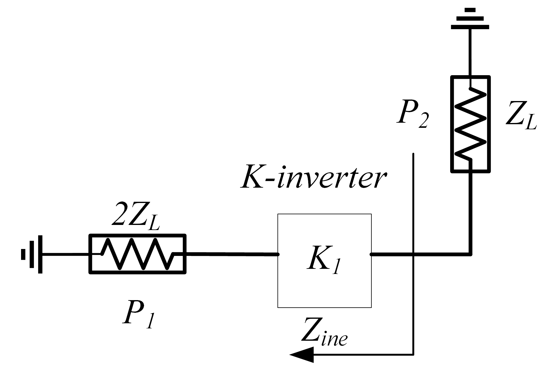
2.1. Analysis of the K-Inverter

Figure 2 shows the equivalent circuit of the K-inverter based on the coupling structure. There are two paths for power transmission between the input and output of the structure; each path consists of two transmission lines with electrical lengths of θ 1 and θ 2 , respectively. Where θ i = 2 π f l i ε e / c , i = 1, 2, ε e denotes the effective dielectric constant, f denotes the operating frequency, l denotes the length of the transmission line, c denotes the speed of light in the free space, and the coupling strength between the two transmission lines is represented by a capacitance C with a very small value. Specifically, the K value of the K-inverter and the positions of the two transmission zeros can be obtained from the following equations [12]:
K = cos θ 1 cos θ 2 2 ω C
f z 1 = c ( 4 l 1 ε e )
f z 2 = c ( 4 l 2 ε e )
where l 1 and l 2 are the lengths of lines θ 1 and θ 2 ; they should satisfy at the operating frequency f 0 :
f 0 c 2 l 1 + l 2 ε e
θ 1 + θ 2 π
Thus, two transmission zeros can be generated at frequencies f z 1 and f z 2 . If l 1 l 2 , it can be found from Equations (1) and (2b) that f z 1 f 0 f z 2 . The two transmission zeros are located at the lower and higher sides of f 0 .
Based on the above analysis, a filtering circuit model is simulated. Rogers 4003 with a dielectric constant of 3.38 and a thickness of 0.81 mm is chosen as the substrate. The simulation results of the equivalent structure are shown in Figure 3, with parameters of θ 1 = 103.5 , θ 2 = 73.4 , and C = 0.036 pF. The results show that the structure can operate as a high-selectivity filter. Moreover, the bandwidth of the structure can be flexibly adjusted by adjusting the values of θ 1 and θ 2 . When the difference between θ 1 and θ 2 becomes lower, the bandwidth also becomes narrower. The simulated bandwidth variations are shown in Figure 4.

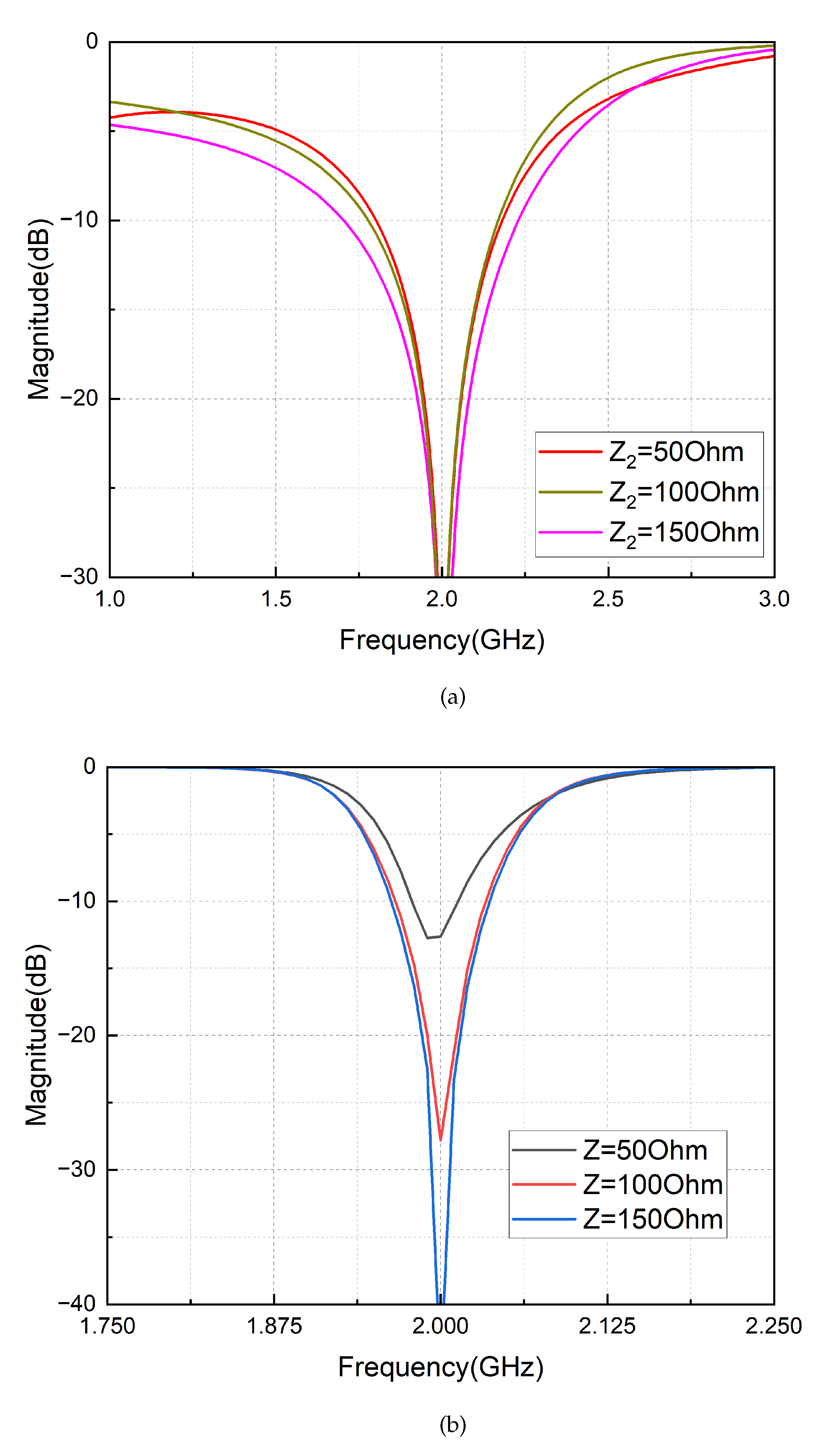
2.2. Analysis of the Even Mode

Figure 5a shows the equivalent circuit of the even mode, with the equivalent impedance divided into two parts: Z i n e 1 and Z i n e 2 . Considering that the K-inverter has a phase shift characteristic of 90 , the following expression can be obtained:
Z i n e 1 = K 1 2 2
Z i n e 2 = Z R 1 + j ω L + j Z tan θ Z + j R 1 + j ω L tan θ
In order to obtain the desired port characteristics of the device, it is necessary to match the impedance to Z L :
Z L = Z i n e 1 / / Z i n e 2
Therefore, it is divided into a real part and an imaginary part:
Re Z i n e 2 = R 1 Z 2 ( 1 + tan 2 θ ) Z ω L tan θ 2 + R 1 2 tan 2 θ
Im Z i n e 2 = Z [ ω L + Z tan θ Z ω L tan θ R 1 2 tan θ ] Z ω L tan θ 2 + R 1 2 tan 2 θ
To reduce the computational effort, the equation itself is processed before the parameters are substituted into Equation (4). When the device is in the even-mode excitation, it is crucial to ensure that all the energy is directed toward the two ports of the power divider rather than being dissipated on the isolation resistors. To simplify the calculation, it is assumed that the real part of the input impedance Z i n e 2 approaches infinite; when the path can be approximated as an open circuit, then there will be no current passing through the resistors. In order to minimize the impact of Z i n e 2 on the power division, it is desirable to maximize the value of Z i n e 2 in Equation (5), requiring a smaller denominator. Thus, it is necessary to satisfy the following condition. In order to achieve this goal, the most direct approach is to set the denominators in Equations (5a) and (5b) to zero. As the denominator is in the form of a sum of squares, the only way to obtain equivalent conditions is to make both factors equal to zero:
Z ω L tan θ 0
Based on Equation (6), the first parameter equation can be obtained as follows:
L Z ω tan θ
Therefore, when the impedance Z of the microstrip line is maximized and the isolation resistance R 1 is minimized, the equivalent impedance can be increased to the greatest extent possible, reducing the impact of the isolation network on power distribution.
However, considering the error and effect in practical applications, in addition to ensuring that Equation (7) is satisfied, it should also make Z as large as possible and the isolation resistance R 1 as small as possible. The larger the value of Z, the better the actual circuit effect, and the impact of the isolation network on the power division will be minimized. This circuit can be simplified into the structure shown in Figure 6; the equivalent impedance of the K-inverter can then be obtained:
Z ine 1 = 1
K 1 = 2

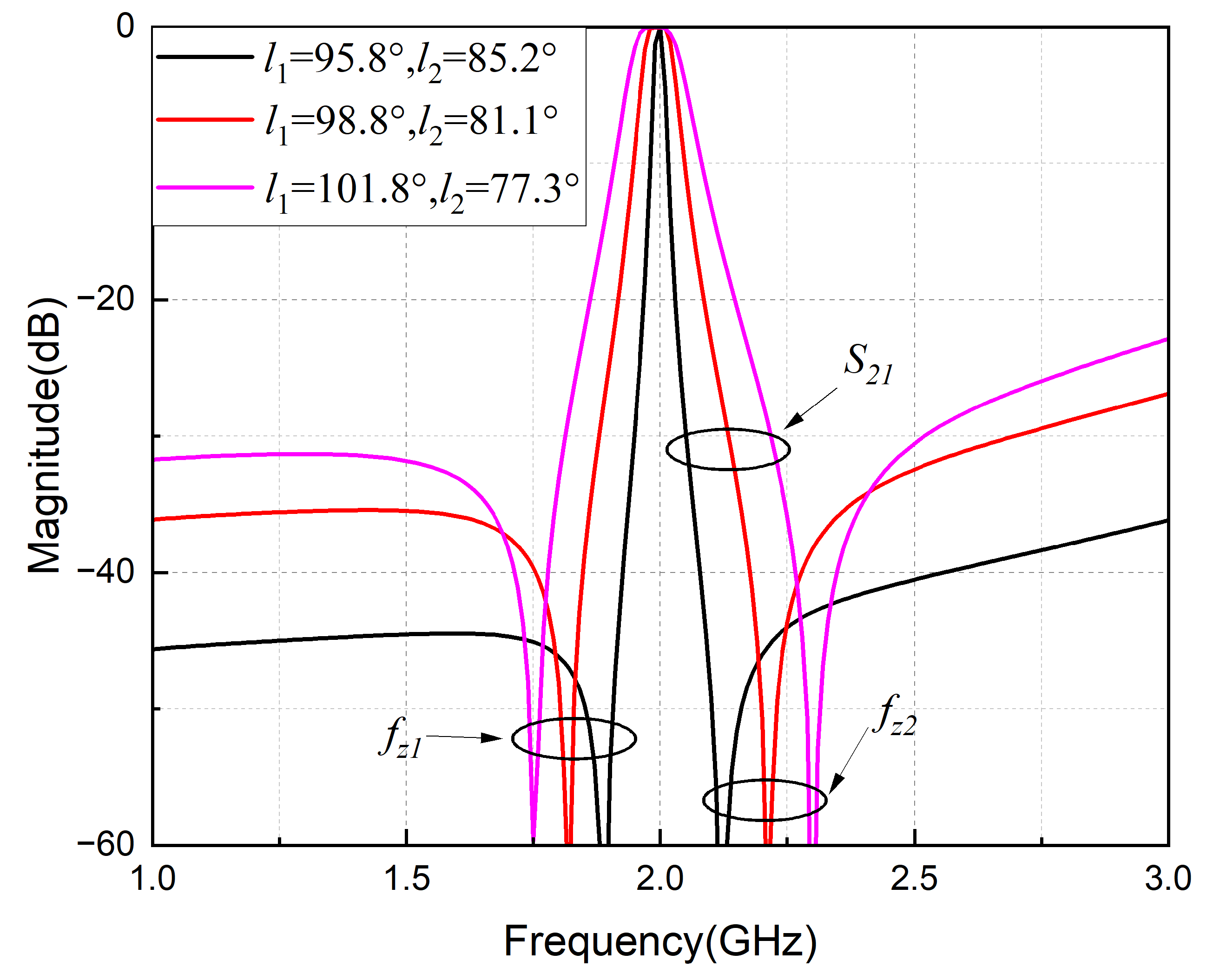
2.3. Analysis of the Odd Mode

In Figure 5b, the odd-mode equivalent circuit of the proposed design is depicted. For ease of calculation, the conductance is used here. Additionally, considering the 90 phase of the K-inverter, Figure 5b can be further simplified to the equivalent circuit in Figure 7.
Before performing the calculations, it is necessary to ensure that the imaginary part of Y i n o 1 is zero, and that R 1 is a value with a purely real part. To simplify the computation, the inductors, capacitors, and transmission lines within the structure are denoted as Part-M. In order to make the resistance, R 1 can change to a value with an imaginary part of 0 after Part-M; the phase characteristic of this impedance transformation structure should be n × 90 , where n = ± 1 , ± 2 ……; the A B C D matrix (9) of this structure is shown as follows:
A M B M C M D M = cos θ j Z sin θ j Y sin θ cos θ 1 2 ω 2 C L j ω L j 4 ω C ( 1 ω 2 C L ) 1 2 ω 2 C L
A M = cos θ 1 2 ω 2 C L 4 ω C Z sin θ 1 ω 2 C L
B M = j ω L cos θ + 1 2 ω 2 C L Z sin θ
C M = j Y sin θ 1 2 ω 2 C L + 4 ω C cos θ 1 ω 2 C L
D M = cos θ 1 2 ω 2 C L ω L Y sin θ W h e r e Y = 1 Z
Theoretically, variable n can take an infinite number of values. In practical applications, it is generally sufficient to consider only two cases: n = 1 or n = 2 , which can cover the remaining cases as well. For each of these two values, one of the following conditions should be satisfied:
A M = D M = 0
B M = C M = 0
When Equation (10a) is satisfied, determining the corresponding value of C results in either 0 or . As neither value is suitable for this structure, Equation (10a) cannot be satisfied.
Case 2 Equation (10b) is analyzed next, where it should satisfy the following:
ω L cos θ + 1 2 ω 2 C L Z sin θ = 0
Y sin θ 1 2 ω 2 C L + 4 ω C cos θ 1 ω 2 C L = 0
After substituting Equation (7) into Equation (11a), we obtain:
C = 1 2 ω Z sin θ cos θ
Next, we replace L and C in Equation (11b) with Equations (7) and (12).
Y sin θ cos 2 θ sin 2 θ + 2 Y 1 sin θ 1 1 2 sin 2 θ = 0
Since Y is not 0 and sin θ is also not 0, Equation (13) can be simplified into the following:
sin 4 θ + sin 2 θ 1 = 0
By the above calculation, the values of capacitance C and the electrical length of the microstrip line in the equivalent structure can be obtained. The characteristic impedance of the microstrip line and the values of the resistors will be calculated in the following sections. Until then, it is assumed that
Y i n o 2 = G + j B
Y i n o 1 = Y G + j B + j Y 1 tan θ Y + j G + j B tan θ W h e r e Y = 1 Z
To satisfy the matching condition, the following can be solved:
G = Y 2 1 + tan 2 θ Y 2 + tan 2 θ
B = Y tan θ 1 Y 2 Y 2 + tan 2 θ
For the equivalent circuit, as shown in Figure 7, the Y i n o 1 expression is shown as follows:
Y i n o 2 = 1 R 1 + j 2 ω C / / 1 j ω L + j 2 ω C
Similar to the analysis above, Y i n o 2 is split into real and imaginary parts:
G = R 1 R 1 2 1 2 ω 2 C L 2 + ω 2 L 2
B = 2 ω C R 1 2 ω L 1 2 ω 2 C L + 2 ω C R 1 2 1 2 ω 2 C L 2 R 1 2 1 2 ω 2 C L 2 + ω 2 L 2
By substituting Equations (7), (12), (17b), to (19b), and simplifying the equation, the following can be obtained:
Z 2 + R 1 2 1 sin 2 θ 1 c o s 2 θ R 1 2 + Z 2 tan 2 θ = Z 2 1 Z 2 tan 2 θ + 1
When Equation (14) holds, 1 sin 2 θ 1 c o s 2 θ 1 . Obviously, it is possible to obtain:
R 1 1
The above analysis of the imaginary part of Y i n o 1 has obtained the value of the resistors, and only the analysis of the characteristic impedance of Z is currently missing, substituting Equations (7), (12), (21), into (19a) to obtain the following:
1 1 + Z 2 tan 2 θ = 1 + tan 2 θ 1 + Z 2 tan 2 θ
This is obviously not true from the exact numerical solution. However, if the value of Z is large enough, it is always possible to make both the left and right sides of the equation approximately equal to 0. In fact, even if the value of Z is only 50 Ω , it is still possible to make the equation approximately valid. To test this hypothesis, simulations of the odd-mode matching performance and the overall structural matching performance for different values of Z are made.
Figure 8 demonstrates that different values of Z can achieve good matching for the odd-mode equivalent circuit. However, for the overall structure, increasing the value of Z results in better return–loss performance. When Z reaches 100 Ω or higher, the overall performance is already quite good. To ensure reliable performance, the value of Z can be selected based on the highest impedance of the corresponding substrate in the subsequent design. It is also advisable to verify the assumptions made for Z in the even-mode analysis in Section 2.2.

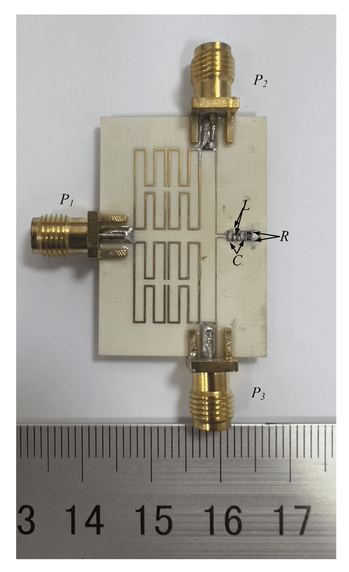
3. Simulation and Measurement of the Circuit

3.1. Design Procedure

Based on the above analysis, the whole design flow is as follows:
  • Determine the required index and frequency of the device, adjust the length and coupling strength of the two transmission lines in the filtering structure by Equations (1a) and (2), and match the equivalent impedance of the structure to 70.7 Ω [12].
  • Take the equivalent impedance of the microstrip line to 150 Ω or other values. Based on the existing frequency, use Equation (7) to calculate the inductance value, Equation (12) to calculate the capacitance value, Equation (14) to calculate the electrical length of the lines, and Equation (21) to calculate the resistance value.
  • Substitute each part into the structure to complete the design.
To verify the above derivation, an equal Gysel FPD operating at 2.1 GHz is designed. Rogers 4003 with a dielectric constant of 3.38 and a thickness of 0.81 mm was chosen as the substrate for this filtering divider. Figure 9 shows the layout of the proposed compact Gysel FPD, where l 1 = 31.5 mm, l 2 = 20 mm, S = 0.25 mm, C = 0.5 pF, L = 10 nH, R = 50 Ω , l = 13.8 mm, and w = 0.12 mm. The capacitor type is Murata GRM1555C2AR50WA01 and the inductor type is Murata LQG15HZ10NG02, both in an 0402 package. A photo of the power divider is shown in Figure 10, with a size of 0.15 λ g * 0.25 λ g .

3.2. Simulated and Measured Results

Figure 11 shows the simulated and measured results of this component, which shows the excellent performance of our designed compact FPD, whose actual operating frequency is at 2.08 GHz and the 3 dB passband is from 1.85 to 2.33 GHz. The input return–loss S 11 is lower than −15 dB in the passband, with a minimum value of −16.75 dB. The insertion loss curves ( S 21 and S 31 ) overlap closely, with a value of −4.02 dB in the passband. The corresponding curves exhibit an insertion loss of 4.02 (3 + 1.02) dB at an operating frequency of around 2.08 GHz, which is relatively low compared to the cascaded structure because it has both the power division and filtering response characteristics.
There are two transmission zeros near the passband, enhancing the frequency selectivity of the filtered power divider. Its isolation is below 15 dB throughout the passband, and the individual ports are well-matched. Finally, the structure can be implemented in other filter forms by ensuring that the filter phase satisfies the special property of 90 ± n × 180 . The size of the proposed design approaches that of the Wilkinson power divider while still retaining the excellent thermal capability of the Gysel power divider. This allows it to operate effectively in high-power applications.

3.3. Comparison

Table 1 presents the comparisons between the compact Gysel FPD proposed in this study and other existing designs. Most of the FPDs listed in the table are based on the Wilkinson topology, which is simpler than Gysel and does not have heat dissipation capabilities, rendering it unsuitable for high-power applications.
From this table, the circuit that we propose offers great performance and a well-matched response. The structure proposed in this study has a significant size reduction over currently existing FPDs. The size of this topology is primarily influenced by the filtering circuit, which significantly reduces the size increase caused by the quarter-wavelength microstrip lines in the Gysel power dividers. Compared to the design of the classic Gysel FPD [12], the insertion loss of this circuit decreases by 0.1 dB, but the size is reduced by approximately 37%, while good port-matching and isolation are achieved. The insertion loss of this structure is 4.0 (3 + 1.0) dB, which is lower than the insertion loss caused by cascading the filter and power divider. This value is good, even for the integrated design. Furthermore, our design incorporates two transmission zeros near the passband, significantly improving the frequency selectivity of the response. With these features, this circuit is useful for size miniaturization and high-power applications.

4. Conclusions

This study presented compact designs of the Gysel topology and an FPD employing a coupling structure. Leveraging the advantages of the lumped components, the circuit size has been significantly reduced, which is much smaller than the existing Gysel FPD. In addition, the theory and experiment show that this structure can effectively integrate the functions of power division and filtering. To verify the calculated circuit parameters, a three-port equal Gysel FPD operating at 2 GHz has been designed and fabricated. The measured results show that the device realizes the integrated design of the filter and power divider in the passband while ensuring good insertion loss and isolation. There are two transmission zeros in addition to the passband, resulting in high selectivity. With these features, this circuit is useful for size miniaturization and high-power applications.

Author Contributions

Conceptualization, Z.W., Z.C. and K.W.; methodology, Z.W. and K.W.; software, Z.W., Z.C. and K.W.; validation, Z.W., Z.C. and K.W.; formal analysis, Z.W. and K.W.; investigation, Z.W. and K.W.; resources, K.W.; data curation, Z.W. and K.W.; writing—original draft preparation, Z.W.; writing—review and editing, Z.W. and K.W.; visualization, Z.W. and K.W.; supervision, K.W.; project administration, K.W.; funding acquisition, K.W. All authors have read and agreed to the published version of the manuscript.

Funding

This work was supported in part by the National Key Research and Development Program of China (no. 2020YFB1807300), the National Natural Science Foundation of China under grant no. 62001140, the Shenzhen Science and Technology Program under grant no. KQTD20210811090116029, the Shenzhen Basic Research Program under grant no. GXWD20201230155427003-20200824201212001, and the Open Research Project of Guangdong Provincial Key Laboratory of Millimeter-Wave and Terahertz (no. 2019B030301002KF2002).

Data Availability Statement

The data can be shared upon request.

Conflicts of Interest

The authors declare no conflict of interest.

References

  1. Chau, W.M.; Hsu, K.W.; Tu, W.H. Filter-Based Wilkinson Power Divider. IEEE Microw. Wireless Compon. Lett. 2014, 24, 239–241. [Google Scholar] [CrossRef]
  2. Liu, Y.; Sun, S.; Zhu, L. 2n-Way Wideband Filtering Power Dividers with Good Isolation Enhanced by a Modified Isolation Network. IEEE Trans. Microw. Theory Tech. 2022, 70, 3177–3187. [Google Scholar] [CrossRef]
  3. Wang, D.; Guo, X.; Wu, W. Wideband Unequal Power Divider with Enhanced Power Dividing Ratio, Fully Matching Bandwidth, and Filtering Performance. IEEE Trans. Microw. Theory Tech. 2022, 70, 3200–3212. [Google Scholar] [CrossRef]
  4. Chen, H.; Zhou, Y.; Zhang, T.; Che, W.; Xue, Q. N-Way Gysel Power Divider with Arbitrary Power-Dividing Ratio. IEEE Trans. Microw. Theory Tech. 2019, 67, 659–669. [Google Scholar] [CrossRef]
  5. Nemati, R.; Karimian, S.; Shahi, H.; Masoumi, N.; Safavi-Naeini, S. Multisection Combined Gysel–Wilkinson Power Divider with Arbitrary Power Division Ratios. IEEE Trans. Microw. Theory Tech. 2021, 69, 1567–1578. [Google Scholar] [CrossRef]
  6. Wen, P.; Ma, Z.; Liu, H.; Zhu, S.; Ren, B.; Song, Y.; Wang, X.; Ohira, M. Dual-Band Filtering Power Divider Using Dual-Resonance Resonators with Ultrawide Stopband and Good Isolation. IEEE Microw. Wireless Compon. Lett. 2019, 29, 101–103. [Google Scholar] [CrossRef]
  7. Liu, Y.; Zhu, L.; Sun, S. Proposal and Design of a Power Divider with Wideband Power Division and Port-to-Port Isolation: A New Topology. IEEE Trans. Microw. Theory Tech. 2020, 68, 1431–1438. [Google Scholar] [CrossRef]
  8. Wang, X.; Ma, Z.; Xie, T.; Ohira, M.; Chen, C.P.; Lu, G. Synthesis Theory of Ultra-Wideband Bandpass Transformer and its Wilkinson Power Divider Application with Perfect in-Band Reflection/Isolation. IEEE Trans. Microw. Theory Tech. 2019, 67, 3377–3390. [Google Scholar] [CrossRef]
  9. Shao, C.; Li, Y.; Chen, J.X. Compact dual-band microstrip filtering power divider using T-junction structure and quarter-wavelength SIR. Electron. Lett. 2017, 53, 434–436. [Google Scholar] [CrossRef]
  10. Zhao, X.L.; Gao, L.; Zhang, X.Y.; Xu, J.X. Novel Filtering Power Divider with Wide Stopband Using Discriminating Coupling. IEEE Microw. Wireless Compon. Lett. 2016, 26, 580–582. [Google Scholar] [CrossRef]
  11. Yu, X.; Sun, S. A Novel Wideband Filtering Power Divider with Embedding Three-Line Coupled Structures. IEEE Access 2018, 6, 41280–41290. [Google Scholar] [CrossRef]
  12. Wang, K.X.; Zhang, X.Y.; Hu, B.J. Gysel Power Divider with Arbitrary Power Ratios and Filtering Responses Using Coupling Structure. IEEE Trans. Microw. Theory Tech. 2014, 62, 431–440. [Google Scholar] [CrossRef]
  13. Shen, G.; Che, W.; Xue, Q.; Feng, W. Novel Design of Miniaturized Filtering Power Dividers Using Dual-Composite Right-/Left-Handed Resonators. IEEE Trans. Microw. Theory Tech. 2018, 66, 5260–5271. [Google Scholar] [CrossRef]
  14. Li, Q.; Zhang, Y.; Wu, C.T.M. High-Selectivity and Miniaturized Filtering Wilkinson Power Dividers Integrated with Multimode Resonators. IEEE Trans. Compon. Packag. Manuf. Technol. 2017, 7, 1990–1997. [Google Scholar] [CrossRef]
  15. Song, K. Compact filtering power divider with high frequency selectivity and wide stopband using embedded dual-mode resonator. Electron. Lett. 2015, 51, 495–497. [Google Scholar] [CrossRef]
  16. Zhang, G.; Wang, J.; Zhu, L.; Wu, W. Dual-Band Filtering Power Divider with High Selectivity and Good Isolation. IEEE Microw. Wireless Compon. Lett. 2016, 26, 774–776. [Google Scholar] [CrossRef]
  17. Chen, M.T.; Tang, C.W. Design of the Filtering Power Divider with a Wide Passband and Stopband. IEEE Microw. Wireless Compon. Lett. 2018, 28, 570–572. [Google Scholar] [CrossRef]
  18. Zhang, X.Y.; Wang, K.X.; Hu, B.J. Compact Filtering Power Divider with Enhanced Second-Harmonic Suppression. Microw. Wireless Compon. Lett. 2013, 23, 483–485. [Google Scholar] [CrossRef]
  19. Wang, Y.; Zhou, C.; Zhou, K.; Wu, W. Compact dual-band filtering power divider based on SIW triangular cavities. Electron. Lett. 2018, 54, 1072–1074. [Google Scholar] [CrossRef]
  20. Deng, Y.; Wang, J.; Li, J.L. Design of compact wideband filtering power divider with extended isolation and rejection bandwidth. Electron. Lett. 2016, 52, 1387–1389. [Google Scholar] [CrossRef]
  21. Mandal, A.; Moyra, T.; Paul, P. Compact Low-pass Filtering-response Wilkinson Power Divider with Wide Harmonic Suppression. In Proceedings of the 2023 IEEE 13th Annual Computing and Communication Workshop and Conference (CCWC), Las Vegas, NV, USA, 8–11 March 2023; pp. 1243–1249. [Google Scholar] [CrossRef]
  22. Huang, F.; Zhu, L. Balanced-to-Unbalanced Filtering In-Phase Power Divider Based on 2-D Patch Resonator. IEEE Microw. Wirel. Technol. Lett. 2023, 33, 399–402. [Google Scholar] [CrossRef]
Figure 1. The equivalent circuit of the proposed Gysel FPD.
Electronics 12 03578 g001
Figure 2. The equivalent circuit of the K-inverter.
Electronics 12 03578 g002
Figure 3. Simulated response of the K-inverter.
Electronics 12 03578 g003
Figure 4. Simulated response of the K-inverter with different bandwidths.
Electronics 12 03578 g004
Figure 5. (a) Even-mode circuit and (b) odd-mode circuit of the proposed FPD.
Electronics 12 03578 g005
Figure 6. The simplified even-mode circuit.
Electronics 12 03578 g006
Figure 7. The simplified odd-mode circuit.
Electronics 12 03578 g007
Figure 8. Performance simulation diagrams for different Z. (a) The matching of the odd mode, (b) S 11 of the whole structure.
Electronics 12 03578 g008
Figure 9. Layout of the Gysel power divider with the filtering response.
Electronics 12 03578 g009
Figure 10. Photographs of the proposed fabricated circuit.
Electronics 12 03578 g010
Figure 11. Simulation and measurement results of the Gysel power divider with filtering responses. (a) S 11 , S 21 , S 31 . (b) S 22 , S 23 , S 33 .
Electronics 12 03578 g011
Table 1. Comparisons between the proposed Gysel FPD and the previous works.
CircuitFreqILISOSizeType
(GHz)(dB)(dB)( λ g × λ g )
[11]3.003.616.50.5 × 0.38Wilkinson
[12]1.963.9190.21 × 0.28Gysel
[14]3.503.9250.17 × 0.30Wilkinson
[15]2.414.2170.45 × 0.45Wilkinson
[20]2.154.3170.59 × 0.295Wilkinson
[21]2.254.3/0.38 × 0.21Wilkinson
[22]44.38230.88 × 0.97Wilkinson
This work2.084.0230.15 × 0.25Gysel
Disclaimer/Publisher’s Note: The statements, opinions and data contained in all publications are solely those of the individual author(s) and contributor(s) and not of MDPI and/or the editor(s). MDPI and/or the editor(s) disclaim responsibility for any injury to people or property resulting from any ideas, methods, instructions or products referred to in the content.

