1. Introduction
Physically unclonable functions (PUFs) work as one-way functions by mapping challenges to responses and can generate cryptographic primitives. They possess inherent randomness derived from manufacturing process inconsistencies, giving rise to their unique and non-reproducible nature [
1]. This distinctive characteristic renders PUFs valuable when used as “digital fingerprints”, which find applications in cybersecurity, including key generation, authentication, and true random number generation (TRNG).
The Internet of Things (IoT) is an emerging communication network that aims to connect many devices. A critical vulnerability of the IoT is that it connects many power-constrained devices. Power-constrained systems, limited in both power consumption and computational power, are often the weakest link in security systems as they present many vulnerabilities, such as key generation, storage, and distribution [
2,
3]. One of the significant advantages of PUFs is that they are well suited for use in power-constrained systems.
The field of cryptography has explored various types of memory PUFs, and among them, the magnetic random-access memory (MRAM) PUF stands out as a particularly promising option. The MRAM PUF is a low-power, non-volatile, high-endurance memory rated for space operation; it is radiation hardened and touted to become the standard for RAM. While numerous MRAM PUFs have been proposed, many have not been tested on low-power client devices and have limited challenge–response pairs (CRPs).
We introduce a novel design for a magnetic random-access memory (MRAM) ternary addressable physically unclonable function (TAPUF). Unlike traditional binary PUFs, this proposed design utilizes trits (three possible states) instead of bits (two possible states). The implementation of this TAPUF utilizes commercially available MRAM devices and it is specifically tailored to run on low-power client devices, thereby demonstrating its compatibility with power-constrained systems.
The main purpose of this research was to collect essential measurements related to the analog characteristics of MRAM devices. These measurements included inter-cell variation, intra-cell variation, medians, and ranges. Additionally, the research investigated specific metrics of the MRAM TAPUF design, such as uniqueness, reliability, and randomness. By analyzing these measurements and metrics, our study aims to offer a comprehensive understanding of the performance and characteristics of the MRAM TAPUF.
The main contributions of this paper are described as follows.
This paper proposes a novel PUF architecture that utilizes two MRAM devices;
We utilized the unstable CRPs to enhance reliability and security;
To address the scaling of CRPs, a technique called “differential read” was employed using MRAM cells from two devices. This approach effectively enhances the scalability of CRPs, allowing for improved performance and reliability in practical applications;
The PUF was implemented on low-power hardware, and the experimental results showed that the PUF had excellent BER, inter-chip Hamming distance, and entropy density.
The rest of this paper is organized into several sections.
Section 2 initiates the discussion by describing the MRAM technology, PUFs, TAPUFs, prior work in the field, and the novel contributions of this study. In
Section 3, we delve into the design of the MRAM TAPUF, explaining the enrollment process and the generation of bits on both the server and client sides.
Section 4 is dedicated to the implementation of the design in hardware. Moving on to
Section 5, the focus shifts to the electrical characterization of the MRAM devices and TAPUF, including evaluating the PUF’s merits, such as uniqueness, reliability, and randomness. In
Section 6, we present an overview of the advantages of our design, along with a comparative analysis of existing work. Finally,
Section 7 concludes the paper by addressing future research directions, identifying areas that require further investigation, and proposing potential avenues for future studies and experiments.
2. Background
2.1. Physically Unclonable Functions
PUFs are physical devices that act as one-way functions by mapping challenges to responses. The term “PUF” was coined in 2002 [
4]; however, the use of physical devices’ intrinsic features as security components dates back as far as 1984 [
5]. PUFs have been widely used since their introduction, with the most popular PUFs being memory PUFs.
A challenge–response pair (CRP) is defined as a PUF’s challenge and subsequent response. A PUF is considered stronger if it has a larger number of CRPs. The threshold between
weak and
strong PUFs is determined by how the number of CRPs scales with size [
6]. If a PUF’s CRPs scale linearly, the PUF is considered
weak; however, if the PUF’s CRPs scale exponentially or quadratically, the PUF is considered
strong.
Memory-based PUFs are a category of PUFs that leverage the inherent cell-to-cell variations of memory devices. They derive their responses from the diverse electrical characteristics of individual memory cells. A variety of memory PUFs have been proposed. The first and most popular are static random-access memory (SRAM) [
7,
8,
9,
10] PUFs. However, emerging memory technologies, such as resistive random-access memory (ReRAM) and MRAM PUFs, have also been proposed in [
11,
12,
13] and [
14,
15,
16,
17], respectively.
A PUF’s response variability might be affected by the environment or aging, making certain responses unstable. In binary addressable PUFs that consist of responses of only 0 s and 1 s, this can become an issue, as some responses might flip between 0 and 1, making them unreliable.
2.2. Ternary Addressable PUF (TAPUF)
A TAPUF or ternary PUF is a variation of a PUF that maps unstable responses to a third state X [
18,
19]. These responses, known as trits, allow for the flagging of unstable bits, so they are not used for authentication purposes or key generation. TAPUFs can lower the bit error rate (BER) by filtering out unstable cells. They can also increase the security of cryptographic protocols obfuscating the process [
20,
21]. Additionally, TAPUFs can leverage their ternary states for true random number generation protocols.
A TAPUF has certain limitations that need to be considered. One drawback is that it requires additional computational power to generate challenges, as the system needs to analyze and classify a larger number of responses. Additionally, it demands more bandwidth to transmit the responses since not all are utilized. Moreover, a mechanism for identifying and communicating unstable responses to the PUF must also be established.
2.3. MRAM Technology
Magnetoresistive random-access memory (MRAM) is an emerging technology that utilizes a magnetic tunnel junction (MTJ) configuration and was initially proposed by Julliere in 1975 [
22]. In this configuration, two ferromagnetic films are separated by a thin insulating material. One of the films is fixed in a specific magnetic orientation, while the other is free to change during programming cycles.
If the insulating material is thin enough, electrons can tunnel through it, effectively creating electrical resistance. This resistance is dependent on the thickness of the insulating material and may be behaviorally modeled as a resistor.
MRAM cells utilize this configuration to store information. The magnetization orientation in the ferromagnetic films is changed to encode data. The electrical resistance exhibited by the MRAM cell determines whether it stores a 0 or a 1. If the magnetic orientations of both films are aligned (parallel configuration), the MRAM cell exhibits lower resistance, a state of 0. Conversely, if the films have different magnetic orientations (anti-parallel configuration), the cell exhibits higher resistance for a 1.
The tunneling magnetoresistance ratio (TMR) refers to the relative change between the high and low resistance states in MRAM. A higher TMR ratio enhances the read capabilities of MRAM, making it easier to differentiate between the high and low states. In MRAM circuitry, CMOS transistors are employed, introducing series resistance typically in the k
range. This series resistance alters the overall relative resistance of MRAM cells. It must be considered when utilizing MRAM as memory or when using its resistance for purposes such as PUF responses. Several studies, including those by Apalkov et al. (2016) [
23] and Vatajelu et al. (2016) [
17], discuss the influence of magnetoresistive effects and considerations in MRAM.
MRAM technology can be classified as toggle, spin-transfer torque (STT), and spin-orbit torque (SOT) MRAM. These classifications are based on the method of writing to memory [
23]. These MRAM cells are shown in
Figure 1.
2.3.1. Toggle MRAM
The first generation of MRAM used a magnetic field to write the state of the MRAM cells. Toggle MRAM is the only first-generation MRAM to remain in production, and it uses the Savtechenko switching method [
24]. A notable advantage of this method is that it grants unlimited write endurance. However, a massive disadvantage to this writing method is that it is more difficult to scale [
23].
2.3.2. STT MRAM
STT MRAM represents the second generation of MRAM. STT uses a current passing between the two ferromagnetic layers, separated by a nonmagnetic spacer, to exert a torque on the magnetization of each layer to flip the free layer [
23,
25]. STT MRAM is capable of large TMRs, making it excellent for memory [
26]. The main advantages of STT MRAM are that it has fast read/write functionality, is easier to scale, and has high reliability.
STT MRAM represents the second generation of MRAM technology. In STT MRAM, a current passes between two ferromagnetic layers separated by a nonmagnetic spacer. This current exerts a torque on the magnetization of each layer, allowing the flipping of the free layer [
23,
25].
STT MRAM is known for its ability to achieve large TMRs, which makes it highly suitable for memory applications, as highlighted in [
26]. One of the key advantages of STT MRAM is its fast read/write functionality, enabling quick data access and modification. Additionally, it offers ease of scalability, meaning it can be efficiently implemented with various memory architectures and sizes. Moreover, STT MRAM exhibits high reliability, ensuring data integrity and long-term operation.
Overall, STT MRAM represents a significant advancement in MRAM technology, combining desirable characteristics, such as fast operation, scalability, and reliability, that make it a promising candidate for memory applications in various computing systems.
2.3.3. SOT MRAM
SOT MRAM is a promising technology that can potentially replace STT MRAM. In SOT MRAM, programming cycles involve applying electric currents parallel to the magnetic tunnel junction [
27]. This programming scheme is different from STT MRAM and is considered gentle, which improves the reliability of read cycles and reduces the likelihood of “read disturbs” occurring.
Additionally, SOT switching in SOT MRAM holds promise for enhancing the speed and endurance of MRAM technology while lowering power [
28]. However, it is important to note that SOT MRAM is still in the developmental stage and not yet ready for large-scale production. Intensive research programs are currently in progress to address challenges such as reducing bit error rates and decreasing the size of the memory cell. These efforts aim to make SOT MRAM a viable and commercially available memory technology in the future.
Figure 1.
Toggle MRAM (
left) [
29], STT MRAM (
middle) [
29], and SOT MRAM (
right) [
27].
Figure 1.
Toggle MRAM (
left) [
29], STT MRAM (
middle) [
29], and SOT MRAM (
right) [
27].
2.4. MRAM PUFs
An early MRAM PUF was proposed in 2014 by Zhang et al. [
30]. This MRAM PUF proposal uses two STT MRAM cells configured as a single PUF cell to generate their response. The STT MRAM cells are configured to a common state (e.g., high or low) and have their electrical resistance compared to generate a 0 or 1. Additionally, an automatic write-back (AWB) scheme is used; the MRAM cell with the lower resistance is written to 0 and the cell with the higher resistance is written to 1 to improve the BER. The researchers simulated this PUF design and presented an inter-distance of 0.501, an entropy calculation of 0.985, and a BER of
. STT MRAM PUF research has been further explored in subsequent studies, such as [
17,
31,
32].
In [
17], the approach involved writing all STT MRAM cells to a common state and tuning the reference current to the median of the responses. This resulted in an equal distribution of 0 s and 1 s. Simulation results demonstrated an inter-distance range of 0.499–0.501, entropy ranging from 0.994 to 0.999, and a BER between 0.05 and 0.07.
In [
31], the authors introduced diode-connected transistors to mitigate the effects of deterioration. Simulations of this proposal exhibited an improved BER of 0, with slight variations occurring under different temperature and voltage conditions, resulting in a BER range of 0.0001–0.0004.
In [
32], the authors put forth an STT MRAM PUF concept that involves comparing the resistances of multiple MTJ cells by passing a current through them. Through simulations, this proposal achieved a BER of 1.56% and a uniqueness metric of 50.0428%.
Another MRAM PUF design was proposed by Das et al. in [
33]. This design used the geometric variations in MTJs to generate responses. In short, the researchers destabilized the MTJs and then released them, and whichever state (i.e., 0 or 1) the MTJ preferred was used as a response. This design was simulated using stochastic LLG, and the design was found to have an inter-distance of 0.47, an entropy calculation of 0.99, and a BER of 0.0225.
Moreover, various MRAM-based TRNGs have been proposed in [
15,
16,
34,
35,
36]. These MRAM TRNGs use STT and toggle MRAM technology to generate truly random numbers with enough entropy to pass the NIST Testing Suite [
37].
2.5. Motivation and Contributions
Many of the MRAM PUF proposals discussed in
Section 2.4 have many shortcomings. First, most designs have CRPs that scale linearly with size, making them weak PUFs. Furthermore, many of these designs have only been simulated in software or rely on wafer-level reads, limiting their practical viability. To the best of our knowledge, our design is the first of its type to be implemented on a low-power client device to emulate real use cases.
Our work builds upon the work in [
38], which used MRAM devices to generate random sequences. This work differs from other MRAM PUF proposals, providing a novel MRAM TAPUF design with CRPs that scale quadratically with size, categorizing it as a strong PUF. The main contributions to this approach are as follows:
A novel design is introduced that uses two different MRAM devices, increasing the number of CRPs;
The PUF is implemented on a low-power device, better simulating actual use cases. This approach allowed us to evaluate the PUF’s performance under realistic conditions and assess its suitability for practical applications.
3. MRAM TAPUF Design
In this design, we exploit the electrical resistances of two MRAM cells obtained from different MRAM devices using a technique called differential cell pairing. This approach allows us to combine and match various MRAM devices, creating a new set of CRPs. Therefore, the number of PUF configurations is , where p is the population of MRAM devices.
The number of CRPs in this design is determined by the square of the MRAM cells on each device, denoted as n. For example, if there are 16 MRAM cells on each device, the number of CRPs would be .
MRAM cells exhibit distinct physical variations among themselves, even when they are programmed to the same state. These variations are reflected in the electrical resistance of the MRAM cells, which is influenced by small physical discrepancies that occur during the manufacturing process.
The MRAM TAPUF follows a specific operational pattern. It receives a challenge from a server accompanied by enrollment information. The challenge comprises a pair of addresses indicating the locations of two MRAM cells. The electrical resistances of these MRAM cells are then converted into two voltages, and a response is generated based on a simple comparison of the voltages. A diagram of this TAPUF design can be found in
Figure 2.
The electrical resistances from a pair of MRAM cells are extracted and used to generate a ternary response (e.g., 0, X, 1). In this process, the locations of the MRAM cells in the pair are the challenge, and the comparison of the cells’ resistance is the response. Additionally, the resistance from each MRAM cell is extracted and then converted to voltage for enrollment and comparison. This is discussed further in
Section 4.
This design has two main steps: enrollment and bit generation.
3.1. Enrollment
To enroll a device, all MRAM cells are written to a common state (high- or low-resistance state). Afterward, each cell’s resistance is measured an r number of times. The average resistance of each cell is stored as the cell’s resistance, and the standard deviation of each cell is stored as the intra-cell variation. MRAM cells with relatively high intra-cell variation are flagged during this phase as unstable cells.
3.2. Bit Generation
To generate cryptographic bits, the server selects random addresses and then sends them to the client. The server utilizes software to compare the resistances of cell pairs in the database and generate an output bit. On the other hand, the client employs physical MRAM devices and analog circuitry to compare the resistances of cell pairs and generate an output bit. In an ideal scenario, the bits generated from the database and those generated from physical measurements should be identical. However, due to random variations in cell queries, there might be practical discrepancies between the two sets of bits.
TAPUFs generate three possible values for each trit: 0, X, or 1. These values are derived from the relative resistance of the TAPUF, which is measured in voltage. The classification of each trit is determined by the voltage difference between the two analog responses of a challenge pair.
Challenge pairs classified as X have a smaller voltage difference than those classified as 0 or 1. The reason for this is that challenge pairs with a smaller voltage difference are more vulnerable to variations in measurements, noise, or external interference. Hence, they are assigned the X classification to indicate their higher susceptibility. The state X is used internally to keep track of the unstable bits, and only states 0 and 1 are used to generate responses.
It is important to note that in the cryptographic protocols that we are studying, the TAPUF only uses the 0 and 1 responses. The X states are filtered internally. At a system level, the TAPUF behaves as a normal binary PUF, with binary streams of responses.
The voltage difference thresholds used to classify trits depend on the specific cryptographic protocol employed. In the context of this paper, the thresholds for trit classification are defined as the responses that fall within the bottom and top 25th percentiles. It is important to highlight that these thresholds can be adjusted to align with the requirements of different protocols.
The equation for bit generation and classification is provided in Equation (
1). In this equation, we utilize
and
to represent the voltage responses obtained from the selected MRAM cells. Additionally,
is used to represent the voltage threshold used for trit classification.
By considering the voltage difference between analog responses and applying appropriate thresholds, TAPUFs are able to classify trits as 0, X, or 1, effectively capturing variations and susceptibility to measurement and environmental factors.
4. Hardware Implementation
4.1. MRAM Device
The MRAM device utilized in this research was the Everspin MR4A16B 54TSSOP version. This commercially available device is organized as 1,048,576 words of 16 bits, providing a high-density memory solution. The MR4A16B employs toggle MRAM cells, which consist of one transistor and one magnetic tunnel junction (MTJ) cell. The MTJ cell comprises two ferromagnetic films with parallel magnetic field orientations. A visual representation of a toggle MRAM cell can be found in
Section 2.3.
The circuit that we designed allowed us to design differential PUFs. By selecting a pair of cells, one from the upper byte and another from the lower byte, and applying a small voltage to the device’s upper (UB) and lower (LB) pins, two currents can be generated. These currents flow from the source into the chosen MRAM cells. The amount of current flowing into a cell makes it possible to analyze particular MRAM cells. Additionally, a small printed circuit board (PCB) adapter was employed to facilitate the easy mixing and matching of multiple devices on a single board.
4.2. Client Device and Additional Hardware
4.2.1. Client Device
We implemented this design on a low-power client device. The Nucleo-1444 H743ZI2 development board was employed because of its low power consumption and quick development time. This development kit has 112 general input/output (GPIO) pins, 2 10–16 bit analog-to-digital converters (ADCs), 3.3 V and 5 V power supplies, and 2 MB of flash memory. This kit’s microcontroller unit (MCU) is the STM32H743ZI2, which operates at 3.3 V and 480 MHz.
4.2.2. Additional Hardware
The currents that enter the MRAM device are used to determine the resistance of the specific cells. To read the MRAM cells and compare them, it is necessary to convert the currents into voltages. Therefore, additional circuitry was required.
A fixed-value resistor was placed in series with the pins connected to MRAM cells. The resistor was placed in series for two reasons. The first reason was limiting the current flowing into the device to prevent internal damage. The second reason was to measure the voltage drop of known resistance in series with the electrical resistance of the MRAM cell, which allowed us to extract the MRAM cell’s relative resistance. Since the voltage drop of the fixed resistor was low (<20 millivolts), a precision amplifier was used to amplify the voltage drop to compare the resistances with greater accuracy.
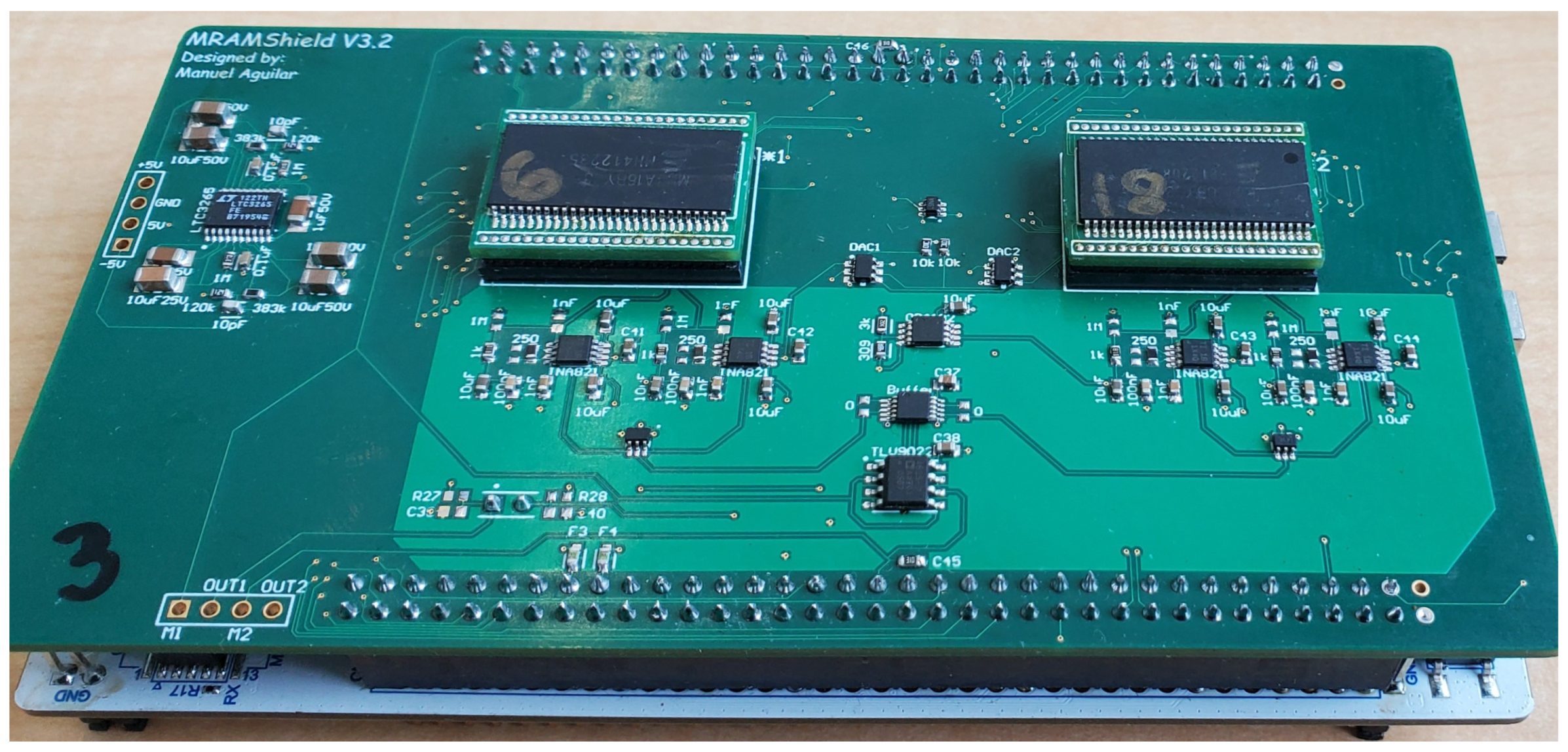
After the voltage drops of the responses were amplified, they were fed to a comparator which output a 0 or 1 depending on which voltage was higher. The comparator was not as crucial to this implementation as the differential amplifier; however, a precise comparator with a fast output swing is preferred. The comparator that was used for this hardware implementation was the ADA4625 op-amp. This op-amp was chosen because it has high precision and a fast output swing. A picture of the hardware circuitry and client device is shown in
Figure 3.
5. Electrical Characterization
5.1. Software
The server was emulated on a personal computer (PC) using python3 and pandas. Enrollment data were collected and stored in CSV files and were accessed using pandas.
The client device was operated using C++ code, which it used to execute any command the server gave. The server and client communication was achieved using pyserial. Using this configuration, we generated responses at a frequency of 33.33 KHz, drawing an average current of 260 mA during key generation. This translated to power consumption of approximately 1.3 W.
5.2. Response Characteristics
To gain a comprehensive understanding of the electrical characteristics of the MRAM devices’ relative resistances, we conducted a thorough analysis involving 30 MRAM devices. In these tests, we examined various parameters, including the mean, intra-cell variation, and inter-cell variation of the cells’ resistance values. Additionally, we evaluated the resistances by testing both the low-resistance and high-resistance states.
For each MRAM device, we performed ten separate reads, each consisting of 10,240 words. The average of these ten reads was considered the cell’s resistance. The intra-cell variation is a measurement that measures the variation in a cell’s resistance over multiple queries. It was calculated by taking the standard deviation of the ten reads.
Inter-cell variation measures the variations in cells within the same device. We assessed the inter-cell variation in the PUF by calculating the standard deviation between the average resistances of MRAM cells in the same device.
Series Resistance
As discussed in
Section 2.3, it is evident that the CMOS circuitry employed for accessing MRAM cells has a significant impact on the resistance obtained from these cells. Upon enrolling multiple devices, we made an intriguing discovery: MRAM cells situated on the same bit-line (such as 0, 1, 2, … 15) exhibited similar resistances. This implies that a cell located on bit
b at address
a will have resistances similar to one on the same bit
b even at a different address
c. This influence can lead to responses that are less “random” with a less-than-normal distribution.
Addressing the influence of the bit-line circuitry on the resistance of each MRAM cell is an important consideration. One approach to tackle this issue is to treat each bit-line as a separate PUF, ensuring that the resistances are independent for each bit-line. However, this approach is limited as it significantly reduces the number of available challenge responses for the PUF and requires carefully selecting MRAM devices with similar relative resistances.
Alternatively, the resistance of all bit-lines can be adjusted to ensure they possess the same median value. This adjustment is necessary to mitigate the impact of the varying bit-line series resistance and maintain consistency in the characteristics of the MRAM cells across different addresses. This method requires additional circuitry and enrollment time but it does not negatively impact the number of CRPs, nor does it require careful device pairing. Furthermore, since the resistances of specific bit-lines are indiscriminately shifted, the overall entropy of the MRAM cells remains unaffected.
Since the relative resistance of cells is measured in the form of a voltage drop, a voltage value can be added to shift the values so that all cells from different bit-lines have the same median values. This adjustment involves selectively modifying the resistances from specific bit-lines to shift their median values. In this study, we achieved this manipulation by incorporating a digital-to-analog converter (DAC) connected to the voltage reference pins of our amplifiers.
Initially, we conducted an enrollment process with a pair of MRAM devices to identify the bit-line with the highest median voltage value. This bit-line was chosen as the reference. Subsequently, all cells from other bit-lines were adjusted upward to achieve an equal median voltage value as the reference bit-line. These adjustments were then saved on the client’s device for future utilization.
Figure 4 compares the relative resistances of a single MRAM device with and without the applied shift in the bit-line median values.
The inter-cell to intra-cell ratio is the inter-cell variation divided by the intra-cell variation. Ideally, we want the inter-cell to intra-cell ratio to be as high as possible to minimize the BER. This means we want to maximize inter-cell variation and minimize intra-cell variation.
As discussed in
Section 5.2, the response statistics must be categorized by bit-line, as the bit-line CMOS series resistance heavily affects the cell’s response.
After enrolling 30 devices in both high- and low-resistance states, the enrollment data showed that, if the average response of a toggle MRAM cell written high (with CMOS series resistance) is T, the responses will range from of T. The average intra-cell variation was only of T, with the average bit-line inter-cell variation being of T, giving an inter-cell to intra-cell variation of 25.03.
The toggle MRAM cells written to a low-resistance state with CMOS series resistance had an average response of , with responses ranging from of L. The average intra-cell variation was of L, with the average bit-line inter-cell variation being of L, giving an inter-cell to intra-cell variation of 25.88.
The response statistics for both states can be found in
Table 1.
The average bit-line inter-cell to intra-cell ratio increased by 0.85 from a high to a low resistance state. Both MRAM states showed excellent statistical values for use as PUFs. While the low-resistance statistical values showed slightly better electrical characteristics, the difference was so minuscule that both states could be used to generate responses.
5.3. PUF Metrics
5.3.1. Inter-Distance
Correlation between MRAM devices can cause security risks, as the responses of one chip can give similar responses to those of other chips. To ensure no correlation between chips, we quantified the inter-chip Hamming distance (
), also known as the inter-distance metric.
is a random variable that describes the distance between two PUF responses to the same challenge for two different PUFs. The inter-distance value of a PUF is also a vital PUF metric as it allows one to quantify the uniqueness of a PUF [
39]. Specifically, it represents the Hamming distance (
) between a stream of responses from two distinct PUFs when subjected to the same challenges. The resulting distance is then divided by the total number of responses to produce the
. Ideally, the
of a PUF should be
0.50. The equation for the
is shown in Equation (
2).
To quantify the value of our PUF design, we carried out an experiment involving the generation of 15 response sequences. Each sequence consisted of a response obtained from a unique PUF configuration, where a configuration was defined as any unique pair of MRAM devices. These responses were acquired from the PUF in both its high- and low-resistance states. Each response sequence was bits long (1 Mb response), ensuring a substantial amount of data for analysis.
Furthermore, as part of our analysis, we generated two sets of sequences: one with unfiltered challenge–response pairs (CRPs) and another with CRPs filtered for X CRPs. We then calculated the average for each set.
For the unfiltered CRPs, the average was found to be 0.4797 in a low-resistance state and 0.4849 in a high-resistance state. On the other hand, for the filtered CRPs, where CRPs classified as X were removed, the average was determined to be 0.4997 in a low-resistance state and 0.4999 in a high-resistance state.
The results of these tests can be found in
Table 2. From these results, we can safely conclude that the responses obtained from both states exhibited similar
values, indicating that the resistive state of the MRAM devices does not significantly impact the uniqueness of the PUF responses.
Filtering ternary states yielded a more desirable value. This indicates that including ternary states in the MRAM PUF responses can introduce a bias towards 0 or 1, reducing the overall uniqueness. In other words, the presence of ternary states in the responses can potentially compromise the distinctiveness of the PUF, highlighting the importance of eliminating or minimizing such states to achieve higher uniqueness and reliability, as well as to minimize error.
5.3.2. Bit Error Rate
The BER is a measurement used to quantify the reliability of a PUF. It is calculated by generating a response sequence from a set of challenges on the client device and comparing it to the response sequence generated with the same set of challenges on the server side. The server uses enrollment data to generate responses, while the client uses the PUF to generate real-time responses. The number of discrepancies between the two sequences divided by the size of the response sequence is the BER.
The BER is similar to the intra-chip Hamming distance (
), which also quantifies the reliability of a PUF. The
of a PUF is a random variable describing the distance between two PUF responses from the same PUF using the same challenge. The BER compares the response of a PUF to that generated from enrollments. A formula for the BER is found in Equation (
3). In this equation, the
is the Hamming distance between a cryptographic key generated on the server using a set of challenges and a cryptographic key generated on the client using the same set of challenges.
Since our responses are in the form of voltages, an important factor in the BER is the settling time allowed for the output signal of the comparator to settle to a state. For most comparators, the slew rate of the output is dependent on the difference between the two inputs; making comparisons between voltages with a small difference requires more time to settle. Theoretically, a higher settling time will lead to more accurate responses as the comparator will have more time to settle into the output, especially with CRPs with small voltage differences.
To quantify the BER, we generated one million responses with different voltage differences, settling times, and resistive states. The voltage differences ranged from 1 to 12 mV in 1 mV steps, and the settling times ranged from 10 to 50
s in 10
s steps. Moreover, each test was performed in a high- and low-resistance state. The plot and values for the BER with the voltage difference, settling time, and resistive state are shown in
Figure 5.
Based on the conducted tests, we observed that, as the voltage difference and settling time increased, the BER decreased, which aligned with our expectations. Surprisingly, the responses generated from a low-resistance state exhibited a noticeably higher error rate compared to those generated from a high-resistance state. This unexpected result suggests that the higher intra-cell variation, measured in millivolts (mV), observed in the low-resistance state contributes to greater instability in the CRPs, resulting in an impact on the BER.
5.3.3. Entropy
Entropy is the measurement of randomness in a system. In cybersecurity applications, entropy quantifies the number of possible key combinations from a PUF’s CRPs, as shown in Equation (
1). In this equation,
E is the number of unique CRPs from a PUF, and
r is the size of the key.
While a PUF may have a large number of CRPs, the responses of a PUF should not be correlated to ensure a high level of security and randomness. Entropy density measures the amount of uncertainty or randomness in a sequence. It is a function of the distribution of the random variable. For PUFs, it represents a generalized and unconditional upper bound on the average predictability of an unobserved response. Ideally, an entropy value as close as possible to 1.00 is desired. To calculate the entropy, we used the Shannon entropy density function shown in Equation (
2) and described in [
40,
41]:
In this equation, represents the probability of the random variable X taking on the value x. The logarithm is usually taken to base 2 () to measure the entropy in bits. The negative sign ensures that entropy is always non-negative. The Shannon entropy measures the average amount of information needed to encode the outcomes of a random variable. It is highest when all outcomes are equally likely, indicating maximum uncertainty, and lowest when there is only one possible outcome, indicating no uncertainty.
To quantify the entropy of our MRAM PUF design, we generated a one million-bit-long key in both low- and high-resistance states. Additionally, we also generated a key filtered for ternary states and an unfiltered key. The results of these tests gave us 0.9994 (low resistance) and 0.995 (high resistance) for unfiltered keys, while yielding 0.99999 (low resistance) and 0.99999 (high resistance) for filtered keys.
5.4. Temperature Testing
Temperature testing is vital in the comprehensive electrical characterization of PUFs. As temperature variations can significantly influence the performance and reliability of electronic devices, it is imperative to evaluate the behavior of PUFs under different thermal conditions.
To assess the robustness and reliability of the PUFs, we conducted comprehensive tests and developed comprehensive characterizations at three different temperatures: 0 C, 23 C, and 80 C. To isolate the impact of temperature on the MRAM devices and exclude the influence if external measurement circuitry, we used flat flex cables and adapters during the temperature tests. This allowed us to focus solely on the temperature effects on the MRAM itself, gaining a clear understanding of its isolated thermal behavior.
By subjecting the PUFs to different temperature ranges and analyzing their responses, we aimed to gain valuable insights into their performance characteristics. This approach allowed us to identify potential vulnerabilities, enhance overall performance, and develop effective calibration or compensation techniques that can be applied when deploying the PUFs in real-world scenarios.
To test varying temperature conditions, we used the Associated Environmental Systems SD-501 temperature chamber. This chamber allowed us to create a wide range of temperature conditions, spanning from −37 C to 180 C. By examining the PUFs’ behavior across different temperature conditions, we could better understand the impact of temperature variations on their reliability and make informed decisions to optimize their operation and ensure their dependable performance in practical applications.
5.4.1. Response Characteristics
To gain a comprehensive understanding of the electrical characteristics of the MRAM PUF across different temperatures, we conducted enrollments with 30 MRAM devices at three specific temperatures: 0
C, 23
C, and 80
C. The detailed results are provided in
Table 3.
Upon analyzing the data, several patterns emerged. Firstly, in the low-resistance state, we observed that, as the temperature increased, the responses also increased. Conversely, in the high-resistance state, as temperature decreased, responses decreased.
Furthermore, we noticed that, as the temperature increased, the variation in the resistance between cells within a single device (intra-cell variation) increased, while the variation in the resistance between different devices (inter-cell variation) decreased. This trend led to a lower inter-cell to intra-cell variation ratio. However, even at 80 C, the inter-cell to intra-cell variation ratio remained higher than 20 for both resistive states, which is more than enough for reliable bit generation.
5.4.2. Bit Error Rate
To evaluate the BER under different temperatures (0 C, 23 C, 80 C), we conducted key generation experiments using the bottom and top 25th percentiles of responses. At each temperature, we generated a total of 1024 keys, each consisting of 1024 bits, which resulted in over one million bits being generated for each temperature. Additionally, for each temperature, a key was generated using the enrollments obtained at each temperature.
During the key generation process, we exclusively utilized state 1, which exhibited greater stability when subjected to lower voltage-pair differences. Moreover, a 20-microsecond settling time was used as it showed a good balance of speed and accuracy.
When using the bottom and top 25th percentiles, the minimum voltage pairs depended on the specific MRAM devices used. For the specific chips used for this test, we obtained voltage pairs with a voltage difference of 11 millivolts or greater.
The results of the BER at different temperatures are presented in
Table 4.
Upon analyzing the results, it became evident that temperature had a slight impact on the BER. As the temperature of the key generation deviated from the temperature at which enrollments were taken, an increase in the BER was noted.
However, this effect can be mitigated by conducting enrollments at various temperatures and selecting the enrollment that is closest to the operating conditions of the client device. By doing so, the impact of temperature on the BER can be minimized.
5.4.3. Uniqueness
To test the uniqueness of the MRAM PUF at different temperatures, we conducted the same tests as those performed at room temperature. Since the resistive state of the MRAM responses did not correlate to the , only high-resistance states were tested. As mentioned earlier, at 23 C, the average was 0.4849 for unfiltered responses and 0.4999 for filtered responses in a high-resistance state.
When the MRAM PUF was exposed to temperatures of 0 C and 80 C, no significant change was observed in the uniqueness of its responses. At 0 C, the average was 0.4820 for unfiltered responses and 0.4999 for filtered responses. Similarly, at 80 C, the average was 0.4753 for unfiltered responses and 0.4997 for filtered responses.
The results of these tests can be seen in
Table 5. From these results, we can conclude that temperature had no significant impact on the
for this PUF configuration.
5.4.4. Entropy
To assess the entropy of the PUF design’s responses under different temperatures, we calculated the Shannon entropy, as discussed in
Section 5.3, at 0
C and 80
C. In this analysis, we focused solely on the responses obtained from the high-resistance states, as the resistive state did not impact the entropy.
At 0 C and 80 C, the Shannon entropy values for unfiltered keys were 0.9982 and 0.9999, respectively. Similarly, for filtered keys, the Shannon entropy values at 0 C and 80 C were both 0.99999. These results led us to the conclusion that temperature did not have a significant effect on the entropy density of the PUF responses. The entropy remained consistent regardless of the temperature at which the responses were generated, reinforcing the stability and reliability of the PUF design in maintaining its entropy characteristics across varying temperatures.
6. Conclusions
We proposed a novel TAPUF design using two MRAM devices. This design uses extracted resistances to produce reliable responses at 33.33 kHz and characterizes analog and digital responses. We enrolled 30 MRAM devices in high- and low-resistance states at varying temperatures and characterized the analog responses. Additionally, we used real-time responses to calculate the and BER of the TAPUF design.
The electrical characterization of the PUF responses provided valuable insights into the PUF’s performance. One important finding was that the CMOS series resistance significantly impacted the PUF responses. However, this issue was successfully addressed by adjusting the PUF responses to ensure they all had the same median value. This modification enabled the MRAM TAPUF to maintain its entropy while accommodating a large number of CRPs ().
Furthermore, the inter-cell to intra-cell variation ratio of the PUF was excellent in both states, indicating consistent behavior across cells. Additionally, minimal difference was observed between the two states. When comparing the two states, the high-resistance state stood out with better metrics, particularly regarding the BER. At a challenge-pair voltage difference of 10 mV and a temperature of 23 C, the high-resistance state demonstrated exceptional performance with an inter-distance value of 0.4998, an entropy value of 0.9999, and a BER below .
Furthermore, this PUF design exhibited reliability across a temperature range of 0 C to 80 C. When enrollments were conducted at the same temperature as used for key generation, the BER remained extremely low. However, as the temperature difference between the enrollment temperature and the key generation temperature increased, an increase in the BER was observed. It is important to note that, even with significant temperature variations, the BER remained within acceptable limits, with a value of at 0 C and 80 C.
Additionally, the entropy and remained close to the ideal values under these temperature conditions. This indicated that the system maintained a reliable level of performance even under varying temperature conditions.
Compared to previously proposed MRAM PUF designs, this particular design demonstrated comparable, if not better, PUF metrics, as shown in
Table 6. These findings highlight the promising performance and reliability of this MRAM PUF design, suggesting its potential superiority over existing designs.
7. Future Plans
In future plans related to this work, the intention is to implement this design using established cryptographic protocols, such as the ternary addressable public key infrastructure [
21] and PUF-seeded post-quantum cryptography [
42]. The objective will be to assess the performance of the design by measuring the latency, the false rejection rate (FRR), and the false acceptance rate (FAR).
Furthermore, it is important to address the vulnerability of certain PUFs to machine learning attacks. Therefore, in order to evaluate the robustness of the MRAM TAPUF design, future work should involve conducting machine learning attacks.
Author Contributions
Conceptualization, M.A.R. and B.C.; Methodology, M.A.R.; Software, M.A.R.; Formal analysis, M.A.R.; Writing—original draft, M.A.R.; Writing—review & editing, M.A.R., M.A. and B.C.; Visualization, M.A.R. and B.C.; Supervision, B.C.; Project administration, B.C.; Funding acquisition, B.C. All authors have read and agreed to the published version of the manuscript.
Funding
This research received no external funding.
Data Availability Statement
The data presented in this study are available in this article.
Acknowledgments
The authors would like to thank Everspin Technologies Inc. for their support in supplying the MRAM devices and the instructions on how to access the MRAM cells directly. The research was sponsored by the Army Research Laboratory and was accomplished under Cooperative Agreement Number W911NF-23-2-0014. The views and conclusions contained in this document are those of the authors and should not be interpreted as representing the official policies, either expressed or implied, of the Army Research Laboratory or the U.S. Government. The U.S. Government is authorized to reproduce and distribute reprints for Government purposes notwithstanding any copyright notation herein.
Conflicts of Interest
The authors declare no conflict of interest.
References
- Gassend, B.L.P. Physical Random Functions. Ph.D. Thesis, Massachusetts Institute of Technology, Cambridge, MA, USA, 2003. [Google Scholar]
- Zanella, A.; Bui, N.; Castellani, A.; Vangelista, L.; Zorzi, M. Internet of things for smart cities. IEEE Internet Things J. 2014, 1, 22–32. [Google Scholar] [CrossRef]
- Meneghello, F.; Calore, M.; Zucchetto, D.; Polese, M.; Zanella, A. IoT: Internet of threats? A survey of practical security vulnerabilities in real IoT devices. IEEE Internet Things J. 2019, 6, 8182–8201. [Google Scholar] [CrossRef]
- Gassend, B.; Clarke, D.; Van Dijk, M.; Devadas, S. Silicon physical random functions. In Proceedings of the 9th ACM Conference on Computer and Communications Security, Washington, DC, USA, 18–22 November 2002; pp. 148–160. [Google Scholar]
- Simmons, G.J. A system for verifying user identity and authorization at the point-of sale or access. Cryptologia 1984, 8, 1–21. [Google Scholar] [CrossRef]
- McGrath, T.; Bagci, I.E.; Wang, Z.M.; Roedig, U.; Young, R.J. A puf taxonomy. Appl. Phys. Rev. 2019, 6, 011303. [Google Scholar] [CrossRef]
- Guajardo, J.; Kumar, S.S.; Schrijen, G.J.; Tuyls, P. FPGA intrinsic PUFs and their use for IP protection. In International Workshop on Cryptographic Hardware and Embedded Systems; Springer: Berlin/Heidelberg, Germany, 2007; pp. 63–80. [Google Scholar]
- Holcomb, D.E.; Burleson, W.P.; Fu, K. Initial SRAM state as a fingerprint and source of true random numbers for RFID tags. In Proceedings of the Conference on RFID Security, Málaga, Spain, 11–13 July 2007; Volume 7, p. 01. [Google Scholar]
- Holcomb, D.E.; Burleson, W.P.; Fu, K. Power-up SRAM state as an identifying fingerprint and source of true random numbers. IEEE Trans. Comput. 2008, 58, 1198–1210. [Google Scholar] [CrossRef]
- Garg, A.; Kim, T.T. Design of SRAM PUF with improved uniformity and reliability utilizing device aging effect. In Proceedings of the 2014 IEEE International Symposium on Circuits and Systems (ISCAS), Melbourne, VIC, Australia, 1–5 June 2014; pp. 1941–1944. [Google Scholar]
- Rose, G.S.; Meade, C.A. Performance analysis of a memristive crossbar PUF design. In Proceedings of the 2015 52nd ACM/EDAC/IEEE Design Automation Conference (DAC), San Francisco, CA, USA, 8–12 June 2015; pp. 1–6. [Google Scholar]
- Pang, Y.; Wu, H.; Gao, B.; Deng, N.; Wu, D.; Liu, R.; Yu, S.; Chen, A.; Qian, H. Optimization of RRAM-based physical unclonable function with a novel differential read-out method. IEEE Electron Device Lett. 2017, 38, 168–171. [Google Scholar] [CrossRef]
- Cambou, B.; Hély, D.; Assiri, S. Cryptography with analog scheme using memristors. ACM J. Emerg. Technol. Comput. Syst. (JETC) 2020, 16, 1–30. [Google Scholar] [CrossRef]
- Vatajelu, E.I.; Di Natale, G.; Prinetto, P. Security primitives (puf and trng) with stt-mram. In Proceedings of the 2016 IEEE 34th VLSI Test Symposium (VTS), Las Vegas, NV, USA, 25–27 April 2016; pp. 1–4. [Google Scholar]
- Ferdaus, F.; Talukder, B.B.; Sadi, M.; Rahman, M.T. True Random Number Generation using Latency Variations of Commercial MRAM Chips. In Proceedings of the 2021 22nd International Symposium on Quality Electronic Design (ISQED), Santa Clara, CA, USA, 7–9 April 2021; pp. 510–515. [Google Scholar]
- Yang, K.; Dong, Q.; Wang, Z.; Shih, Y.C.; Chih, Y.D.; Chang, J.; Blaauw, D.; Svlvester, D. A 28NM integrated true random number generator harvesting entropy from MRAM. In Proceedings of the 2018 IEEE Symposium on VLSI Circuits, Honolulu, HI, USA, 18–22 June 2018; pp. 171–172. [Google Scholar]
- Vatajelu, E.I.; Natale, G.D.; Barbareschi, M.; Torres, L.; Indaco, M.; Prinetto, P. STT-MRAM-based PUF architecture exploiting magnetic tunnel junction fabrication-induced variability. ACM J. Emerg. Technol. Comput. Syst. (JETC) 2016, 13, 1–21. [Google Scholar] [CrossRef]
- Yamamoto, D.; Sakiyama, K.; Iwamoto, M.; Ohta, K.; Ochiai, T.; Takenaka, M.; Itoh, K. Uniqueness enhancement of PUF responses based on the locations of random outputting RS latches. In International Workshop on Cryptographic Hardware and Embedded Systems; Springer: Berlin/Heidelberg, Germany, 2011; pp. 390–406. [Google Scholar]
- Cambou, B.; Orlowski, M. PUF designed with Resistive RAM and Ternary States. In Proceedings of the 11th Annual Cyber and Information Security Research Conference, Oak Ridge, TN, USA, 5–7 April 2016; pp. 1–8. [Google Scholar]
- Cambou, B.; Flikkema, P.G.; Palmer, J.; Telesca, D.; Philabaum, C. Can ternary computing improve information assurance? Cryptography 2018, 2, 6. [Google Scholar] [CrossRef] [Green Version]
- Assiri, S.; Cambou, B.; Booher, D.D.; Miandoab, D.G.; Mohammadinodoushan, M. Key exchange using ternary system to enhance security. In Proceedings of the 2019 IEEE 9th Annual Computing and Communication Workshop and Conference (CCWC), Las Vegas, NV, USA, 7–9 January 2019; pp. 488–492. [Google Scholar]
- Julliere, M. Tunneling between ferromagnetic films. Phys. Lett. A 1975, 54, 225–226. [Google Scholar] [CrossRef]
- Apalkov, D.; Dieny, B.; Slaughter, J.M. Magnetoresistive random access memory. Proc. IEEE 2016, 104, 1796–1830. [Google Scholar]
- Savtchenko, L.; Engel, B.N.; Rizzo, N.D.; Deherrera, M.F.; Janesky, J.A. Method of Writing to Scalable Magnetoresistance Random Access Memory Element. U.S. Patent 6,545,906, 8 April 2003. [Google Scholar]
- Slonczewski, J.C. Current-driven excitation of magnetic multilayers. J. Magn. Magn. Mater. 1996, 159, L1–L7. [Google Scholar] [CrossRef]
- Wang, M.; Cai, W.; Cao, K.; Zhou, J.; Wrona, J.; Peng, S.; Yang, H.; Wei, J.; Kang, W.; Zhang, Y.; et al. Current-induced magnetization switching in atom-thick tungsten engineered perpendicular magnetic tunnel junctions with large tunnel magnetoresistance. Nat. Commun. 2018, 9, 671. [Google Scholar]
- Prenat, G.; Jabeur, K.; Di Pendina, G.; Boulle, O.; Gaudin, G. Beyond STT-MRAM, spin orbit torque RAM SOT-MRAM for high speed and high reliability applications. Spintron.-Based Comput. 2015, 145–157. [Google Scholar] [CrossRef]
- Wang, M.; Cai, W.; Zhu, D.; Wang, Z.; Kan, J.; Zhao, Z.; Cao, K.; Wang, Z.; Zhang, Y.; Zhang, T.; et al. Field-free switching of a perpendicular magnetic tunnel junction through the interplay of spin–orbit and spin-transfer torques. Nat. Electron. 2018, 1, 582–588. [Google Scholar] [CrossRef]
- Everspin Technologies, Inc. Available online: https://www.everspin.com/ (accessed on 24 July 2023).
- Zhang, L.; Fong, X.; Chang, C.H.; Kong, Z.H.; Roy, K. Highly reliable memory-based physical unclonable function using spin-transfer torque MRAM. In Proceedings of the 2014 IEEE International Symposium on Circuits and Systems (ISCAS), Melbourne, VIC, Australia, 1–5 June 2014; pp. 2169–2172. [Google Scholar]
- Lim, S.; Song, B.; Jung, S.O. Highly independent MTJ-based PUF system using diode-connected transistor and two-step postprocessing for improved response stability. IEEE Trans. Inf. Forensics Secur. 2020, 15, 2798–2807. [Google Scholar] [CrossRef]
- Hu, Y.; Wu, L.; Chen, Z.; Huang, Y.; Xu, X.; Li, K.; Zhang, J. STT-MRAM-Based Reliable Weak PUF. IEEE Trans. Comput. 2022, 71, 1564–1574. [Google Scholar] [CrossRef]
- Das, J.; Scott, K.; Rajaram, S.; Burgett, D.; Bhanja, S. MRAM PUF: A novel geometry based magnetic PUF with integrated CMOS. IEEE Trans. Nanotechnol. 2015, 14, 436–443. [Google Scholar]
- Vatajelu, E.I.; Di Natale, G. High-Entropy STT-MTJ-Based TRNG. IEEE Trans. Very Large Scale Integr. (VLSI) Syst. 2019, 27, 491–495. [Google Scholar] [CrossRef]
- Perach, B. An asynchronous and low-power true random number generator using STT-MTJ. IEEE Trans. Very Large Scale Integr. (VLSI) Syst. 2019, 27, 2473–2484. [Google Scholar] [CrossRef]
- Vatajelu, E.I.; Di Natale, G.; Prinetto, P. STT-MTJ-based TRNG with on-the-fly temperature/current variation compensation. In Proceedings of the 2016 IEEE 22nd International Symposium on On-Line Testing and Robust System Design (IOLTS), Sant Feliu de Guixols, Spain, 4–6 July 2016; pp. 179–184. [Google Scholar]
- Bassham, L.; Rukhin, A.; Soto, J.; Nechvatal, J.; Smid, M.; Leigh, S.; Levenson, M.; Vangel, M.; Heckert, N.; Banks, D. A Statistical Test Suite for Random and Pseudorandom Number Generators for Cryptographic Applications; US Department of Commerce, Technology Administration, National Institute of Standards and Technology: Gaithersburg, MD, USA, 2010.
- Derlecki, M.; Siwiec, K.; Narczyk, P.; Pleskacz, W.A. Design of a true random number generator based on MRAM devices. Comput. Conf. 2023; in press. [Google Scholar]
- Maes, R. Physically Unclonable Functions: Constructions, Properties and Applications; Springer Science & Business Media: New York, NY, USA, 2013. [Google Scholar]
- Maes, R.; Van Herrewege, A.; Verbauwhede, I. PUFKY: A fully functional PUF-based cryptographic key generator. In Proceedings of the Cryptographic Hardware and Embedded Systems—CHES 2012: 14th International Workshop, Leuven, Belgium, 9–12 September 2012; Proceedings 14. Springer: Berlin/Heidelberg, Germany, 2012; pp. 302–319. [Google Scholar]
- Taneja, S.; Rajanna, V.K.; Alioto, M. 36.1 unified in-memory dynamic TRNG and multi-bit static PUF entropy generation for ubiquitous hardware security. In Proceedings of the 2021 IEEE International Solid-State Circuits Conference (ISSCC), San Francisco, CA, USA, 13–22 February 2021; Volume 64, pp. 498–500. [Google Scholar]
- Cambou, B.; Gowanlock, M.; Yildiz, B.; Ghanaimiandoab, D.; Lee, K.; Nelson, S.; Philabaum, C.; Stenberg, A.; Wright, J. Post Quantum Cryptographic Keys Generated with Physical Unclonable Functions. Appl. Sci. 2021, 11, 2801. [Google Scholar] [CrossRef]
| Disclaimer/Publisher’s Note: The statements, opinions and data contained in all publications are solely those of the individual author(s) and contributor(s) and not of MDPI and/or the editor(s). MDPI and/or the editor(s) disclaim responsibility for any injury to people or property resulting from any ideas, methods, instructions or products referred to in the content. |
© 2023 by the authors. Licensee MDPI, Basel, Switzerland. This article is an open access article distributed under the terms and conditions of the Creative Commons Attribution (CC BY) license (https://creativecommons.org/licenses/by/4.0/).


