1. Introduction
PCB stands for printed circuit board. The bare board of a PCB is usually rectangular, and the front and back sides are usually sprayed green or other coloured protective varnish. Only bare, round, hole-shaped pads are used for soldering the electronic components. The front of the PCB will be painted to indicate the wiring connection between the pads, indicating the connection between the pads. For ease of assembly, the PCB surface is also marked with the name and model number of the electronic components assembled in that position. Instead of intricate wires connecting tiny components, PCBs have the necessary electronic components and have the advantages of densification and high reliability, designability, and producibility. In the electronic information manufacturing industry, soldering electronic components to PCBs can reduce product size and production costs and increase production efficiency, which is important as this increases output and product quality. Both household appliances and military weapon systems use PCBs as the medium for electrical interconnection, and today, PCBs are used in almost all electronic products.
Considering the wide range of PCB applications, which includes advanced computers, automated driving, and objects related to aerospace and other highly sophisticated fields, the PCB quality can directly affect the operation of devices, so increasing the PCB quality is of high importance to the electronic information industry. Detecting surface defects in PCBs is a key element in increasing the quality of electronic products. To ensure high-quality products, individuals avoid using poorly assembled products by screening out PCBs with surface defects. The various defects present on PCBs can be broadly divided into solder and non-soldering defects [
1], which can be subdivided into wiring trace faults, polarity errors, missing components, and component misalignments [
2,
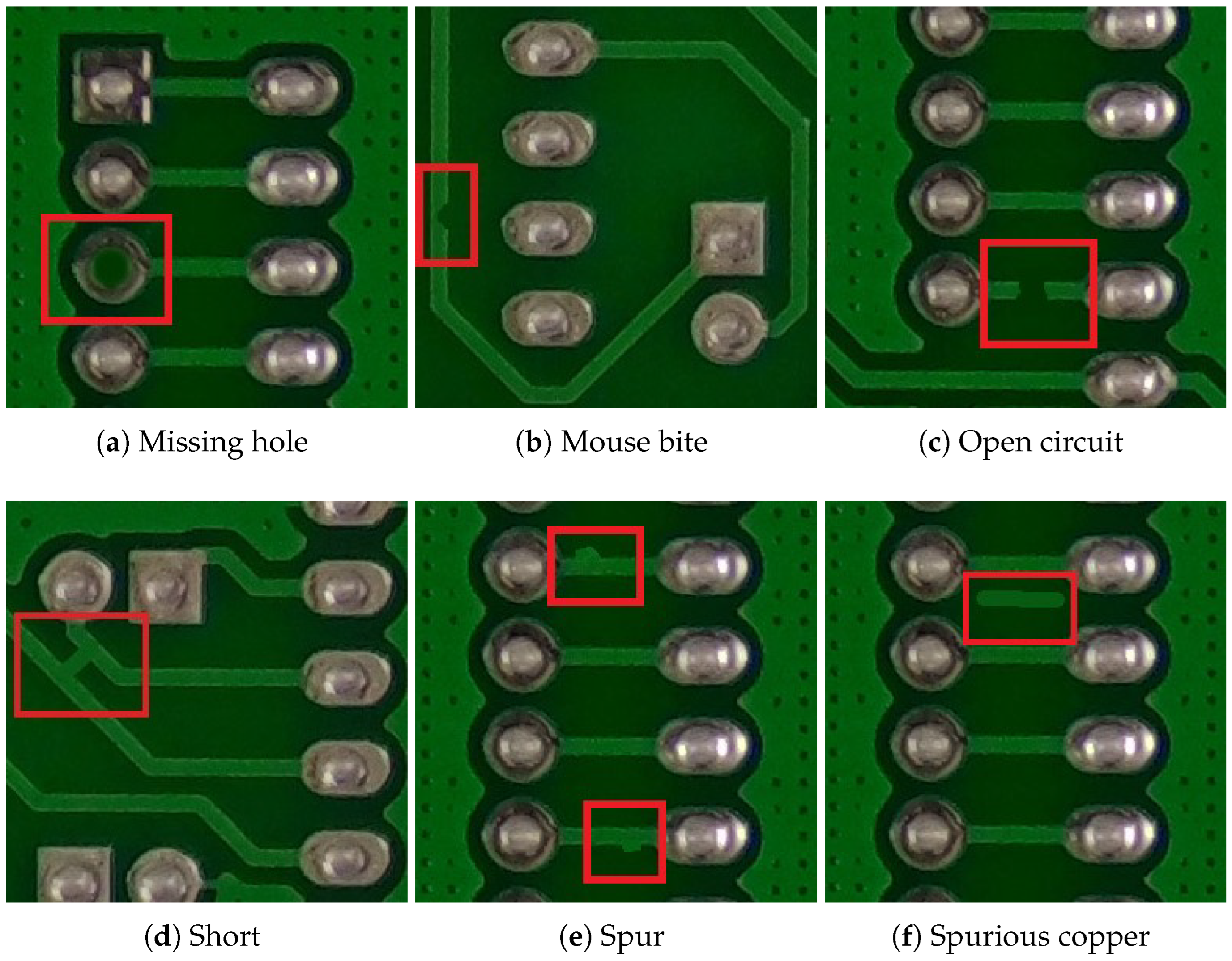
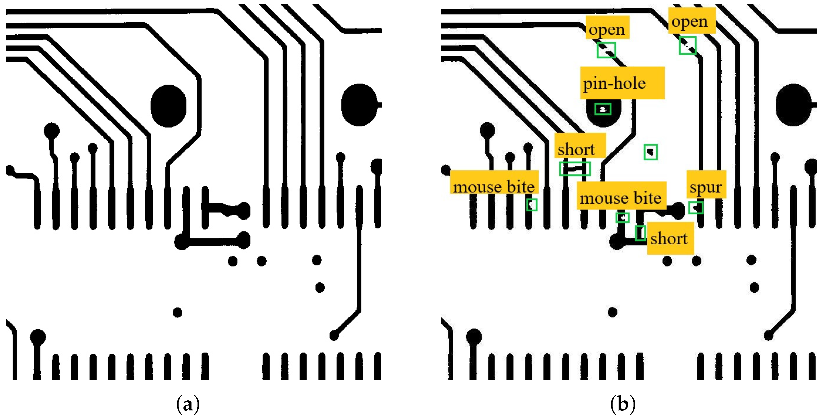
3]. The object of study for this experiment was the PCB bare board surface defects that belonged to a wiring track fault that contained six types of defects: missing holes, mouse bites, open circuits, shorts, spurs, and spurious copper, as shown in
Figure 1.
The traditional methods used to detect PCB surface defects include the naked eye and probe detection methods. The former is mainly performed by observing PCB surface defects with the naked eye, but this method requires inspectors to have a plethora of experience, and making these observations for a long time leads to adverse effects on the accuracy and efficiency of the detection. The latter is mainly performed by using a needle bed or flying needle equipment with a computer to edit the test program, control the probe and PCB for contact, and determine whether surface defects exist according to the data from the PCB probe analysis, but this method requires more expensive equipment and higher learning costs, and the detection process will cause damage to the PCB. Therefore, ensuring efficiency and accuracy in a batch inspection environment is difficult when using traditional inspection methods; thus, a method whereby users can more accurately and efficiently detect surface defects on PCBs is needed.
Applying noncontact automatic optical inspection methods to detect PCB surface defects is now a major research focus, and high-resolution optical sensors and image-processing algorithms are used to detect surface defects on PCBs [
4], both via traditional image-processing and deep-learning-based detection methods.
Regarding the traditional image-processing detection methods, Mukesh Kumar et al. proposed a method to detect PCB bare board defects by combining image enhancement techniques and a standard template generation particle analysis [
5]. Khlong Luang and Pathum Thani proposed a PCB defect classification method by using arithmetic and logical operations, a circular hough transform (CHT), morphological reconstruction (MR), and connected component labelling (CCL) [
6]. Liu and Qu used a hybrid recognition method of mathematical morphology and pattern recognition to process PCB images and used an image aberration detection algorithm to mark images of PCB defects for defect identification [
7]. Gaidhane et al. introduced the concept of linear algebra to determine the presence of surface defects in PCBs by calculating the rank of the matrix corresponding to the image [
8]. Although these methods can be used to achieve satisfactory accuracy, the detection rate is slow, which is not conducive to fast detection in practical applications. Moreover, they are dependent on a priori knowledge or require a large number of standard images to be stored, which is not conducive to generalization to different scenarios [
9].
The deep learning approach to detection is based on a model trained by a neural network to detect defects; firstly, the object detection weight is trained, which involves building and labelling the dataset, designing the neural network structure, and setting the training parameters and strategy. During the training process, the weight parameters are updated after backpropagation, with the loss values of the model tending to decrease and the accuracy values tending to increase, and the performance of the resulting weight can be evaluated by using either a validation or test set after training is complete. The detection of surface defects on PCBs by using deep learning object detection methods has been shown to be feasible by the results of several studies. Ding et al. proposed a tiny defect detection network, TDD-Net, which exploits the inherent multiscale and pyramidal hierarchy of deep convolutional networks when constructing feature pyramids with high portability [
10]. Hu et al. modified a Faster-RCNN by using ResNet50 as the backbone network and fusing the GARPN and ShuffleNetV2 residual units [
11]. Liao et al. enhanced the YOLOv4 network to obtain YOLOv4-MN3, replaced the CSPDarkNet53 backbone network with MobileNetV3, added the SENet attention to the neck network, optimized the activation and loss functions, and constructed a dataset by capturing 2008 images containing PCB surface defects of 4024 × 3036 pixels with an industrial camera; the dataset contained six types of surface defects: bumpy or broken lines, clutter, scratches, line-repair damage, hole loss, and over oil filling. The weight was used to detect these six types of PCB surface defects with a mAP of 98.64% and FPS of 56.98 [
9]. Zheng et al. proposed an enhanced full convolutional neural network based on MobileNet-V2 by incorporating atrous convolution and enhancing the skip layers, and the average recognition accuracy of this network when detecting four PCB defects was 92.86% [
12]. However, the networks proposed in the literature [
10,
11,
13] all suffer from slow detection rates and a lack of efficiency.
To solve the current problem of the lack of accuracy, efficiency, and stability of the PCB surface defect detection methods that are used in industrial production, we introduce deep learning methods and computer vision technology, a neural-network-based object-detection method that allows PCB surface defects to be automatically identified by using YOLOv5 as the framework is used, and we propose YOLO-MBBi based on YOLOv5. YOLO-MBBi contains the following enhancements to the YOLOv5 network: the backbone network of YOLOv5s is replaced with an MBConv (mobile inverted residual bottleneck block), the main module of EfficientNet-B0 is used, the baseline network of EfficientNet [
14] has a superior inference rate and accuracy, the CBAM [
15] attention is added to enhance the feature learning of the objects in the backbone network, BiFPN [
16] is added in the head detector feature fusion network, some of the convolutions in the detection head network are replaced with depth-wise convolutions [
17], and the CIoU loss function that was originally used in YOLOv5 is replaced with the SIoU loss function to enhance the learning [
18]. Finally, an optimized weight is obtained by training using the YOLO-MBBi network structure, which is used to detect the PCB surface defects and compare YOLO-MBBi with other neural networks, including the original YOLOv5s.
2. Related Works
YOLO, which stands for you only look once [
19,
20,
21,
22], is a one-stage object-detection network that differs from two-stage object-detection networks such as R-CNN and Faster-R-CNN [
23,
24] in that the YOLO series of networks only needs to scan the image once to output the detection result, which achieves the function of object localization and detection at one time, whereas two-stage object detection networks need to scan the image twice to complete object localization and detection. Therefore, although the detection accuracy of the YOLO series networks may be slightly inferior to that of the first-stage object-detection network, YOLO series networks are faster in terms of their detection rate and still achieve an excellent accuracy, which has a high theoretical and application value; additionally, many scholars have found results related to object detection by using YOLO series networks to enhance the network [
25,
26,
27,
28].
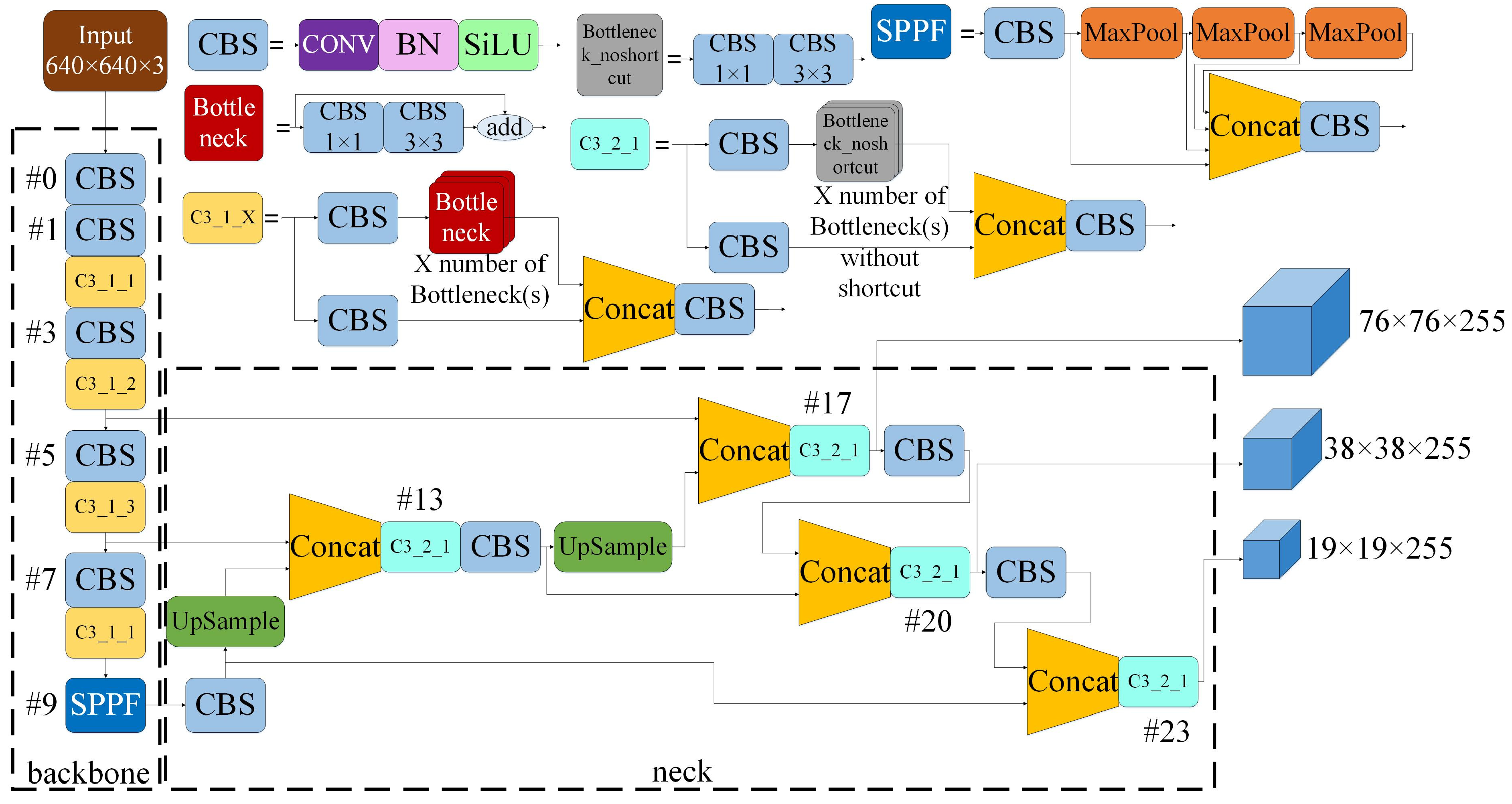
YOLOv5 is the fifth iteration of the YOLO series network, which is now divided into five versions in terms of their weight, from small to large, depth, and width. The network depth increases according to the number of modules in the series, and increasing the network depth allows for a larger receptive field to help capture more pixel-like features and increase the expressiveness of the model. Increasing the number of input and output channels between layers increases the network width, and increasing the network width allows for finer granularity and richer features and increases the parallelism of the model, which thereby increases the training speed. As a result, the number of modules used for smaller weights is overall smaller than the number used for larger weights, so smaller weights are faster but less accurate, whereas larger weights are slower but more accurate, and the training cost rises as the depth and width of the weight increases. The YOLOv5s v6.0 network was chosen to enhance and test the PCB surface defect detection, and we needed to ensure both the detection efficiency and accuracy of the network, as these factors are most important for practical application scenarios. The YOLOv5s versions mentioned below are all v6.0.
The YOLOv5s network structure is shown in
Figure 2. The structure consists of three main parts, namely the backbone and neck network and head detector. The backbone network consists of a convolution module named CBS that is connected by a convolution, batch normalization layer, SiLU activation function [
29], and C3_1 modules that contain a residual structure in a series. The role of the convolution module is to obtain the feature map in the original image by downsampling, and the residual structure in the C3_1 module can enhance the gradient value during backpropagation, which effectively prevents the gradient from disappearing when the network deepens and reduces the loss in feature extraction. The SPP (spatial pyramid pooling) [
30] module is the last layer of the old YOLOv5s backbone network. The current version of YOLOv5s uses the SPPF module to replace the SPP module used in the previous version, which is optimized on the basis of SPP and reduces the computational effort and increases the computational speed of the model without changing the original algorithm. The module downsamples the last layer of the feature map with three different-sized convolution layers and fuses the three downsampled features to extract spatial features of different sizes and to increase the robustness of the model. The next subnetwork connected to the backbone network is the neck network, which mainly consists of convolution, upsampling, feature fusion, and C3_2 modules with the residual structure removed. The feature fusion module can concatenate feature maps of the same size in both layers of the network to increase the number and granularity of the features in the feature map. C3_2 reuses the C3_1 module from the backbone network, which reduces the computational effort, enhances the feature fusion capability, and retains richer feature information. Lastly, the output section of YOLOv5s uses CIoU as the loss function and provides three different feature map sizes for detection.
3. Network Enhancement Methodology
For this study, five aspects of YOLOv5s were enhanced: the backbone network, attention module, feature fusion, loss function, and convolution substitution. The following section describes the details of the enhanced approach and illustrates the advantages of the enhanced modules used.
3.1. Backbone Network Enhancement
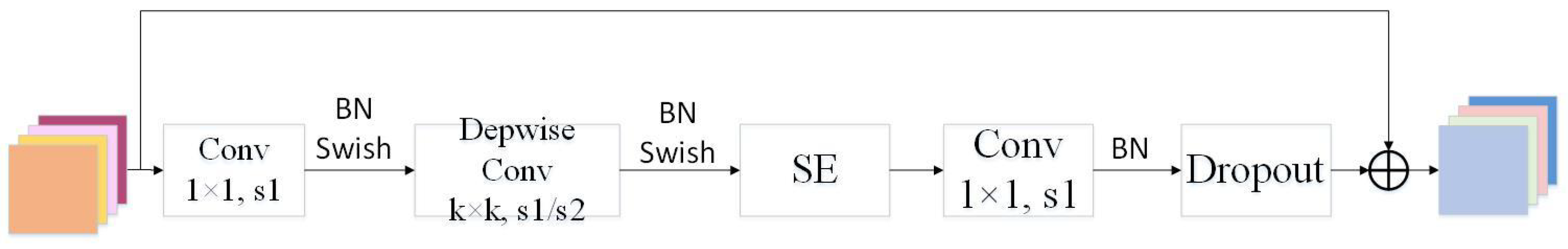
Tan and Le proposed EfficientNet [
14] after studying the effect of varying the width, depth, and resolution of the input image of the neural network on the detection accuracy and network rate. EfficientNet includes the EfficientNet-B0 baseline weight and seven weights proposed on the basis of the baseline according to the size from small to large. For this study, the main MBConv module of the EfficientNet-B0 baseline weight was chosen, which was obtained by searching through the neural network architecture whose structure is shown in
Figure 3. The module performs a 1 × 1 point-by-point convolution of the input feature map and changes the channel dimension of the output feature map according to the expansion parameters, and adds an SE attention mechanism to recover the channel number of the original feature map again with a 1 × 1 point-by-point convolution.
An MBConv is a lightweight convolutional operation that can reduce computation and memory consumption and maintain high accuracy. It employs multiple cross-layer connections and attention mechanisms to increase the robustness and generalization ability of the model, which causes it to be lightweight, efficient, and scalable for high-accuracy image classification and object-detection tasks. For this experiment, an MBConv was used in the backbone network to replace the CBS and C3 modules used by YOLOv5s.
3.2. CBAM Attention
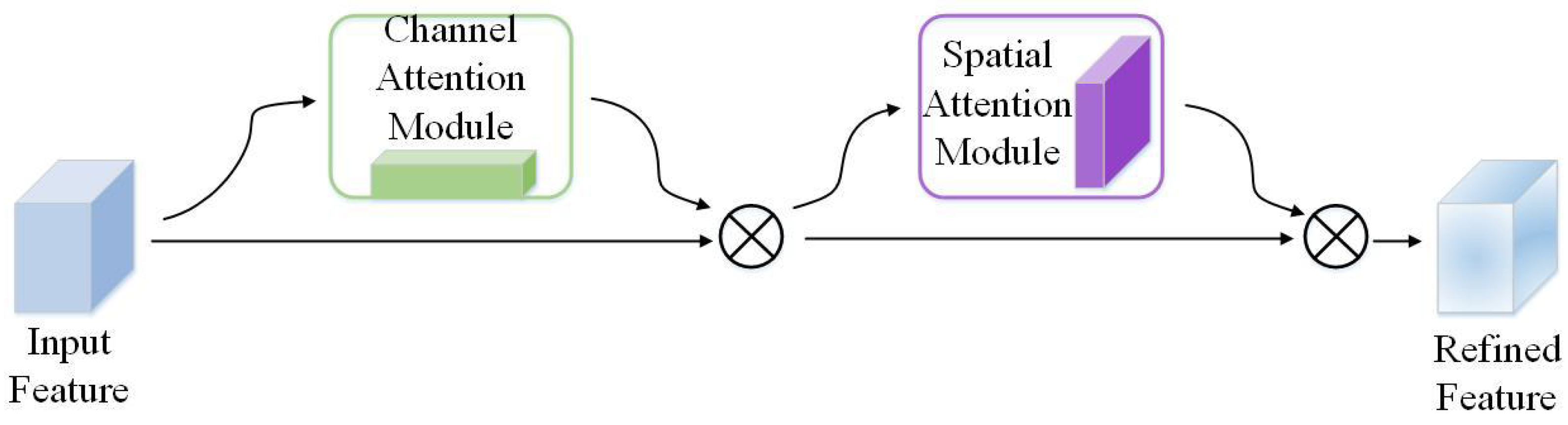
The CBAM attention links channel and spatial attention in series. These two attention modules will infer input feature maps in turn and then multiply the attention maps according to the input feature maps to perform an adaptive feature modification. Its structure diagram is shown in
Figure 4. The CBAM module is lightweight and versatile, can be integrated into any CNN architecture with negligible overhead, and can be trained alongside CNNs.
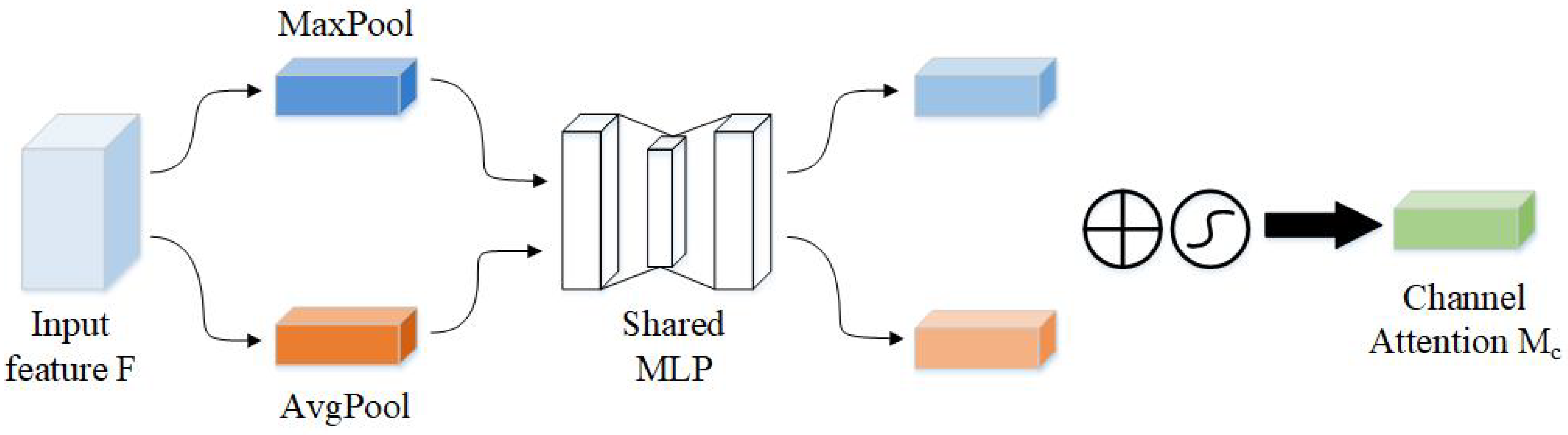
Regarding the main method that is used to process the feature map by using CBAM attention, the feature map is first max and average pooled by the channel attention module to calculate two tensors with only the channel dimensions, which are summed by a fully connected layer and activated by a sigmoid function to obtain the channel attention tensor; the channel attention structure is shown in
Figure 5, and its expression is shown in Equations (
1) and (
2).
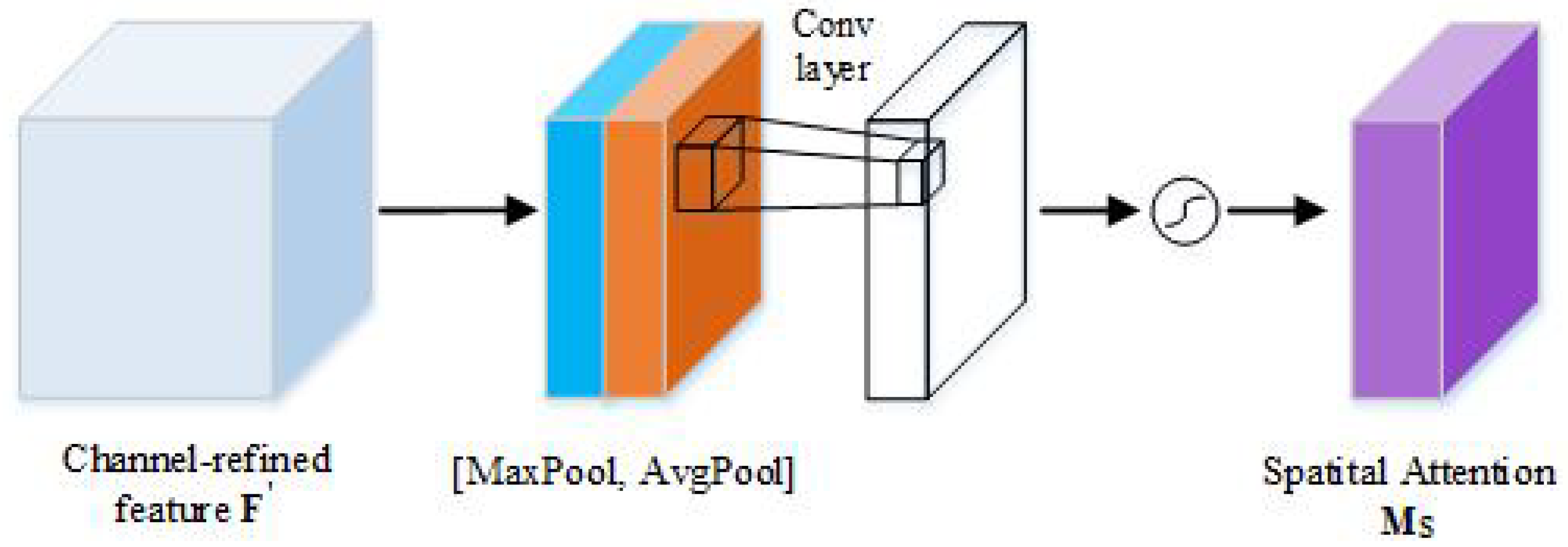
The new feature maps are calculated by the channel attention module and then passed through the spatial attention module. The spatial attention module pools the feature maps of the maximum and average pooling and connects the two pooled tensors in the channel dimension. The spatial attention tensor is obtained by convolving the obtained feature maps into one channel and then activating it with the sigmoid function. The structure of the spatial attention is shown in
Figure 6, and its expression is shown in Equation (
3).
The CBAM attention can adaptively select and adjust the feature information of the input data to help the neural network more accurately capture the important feature information from the input data, which thus increases the accuracy of the model. It can also compress and streamline the parameters and computation in the neural network by adaptively adjusting the feature weights of the input data, which thus reduces the size and computational complexity of the model. The addition of the CBAM attention can enhance the performance and computational efficiency of the neural networks, which thus makes them more applicable in various application scenarios. So, CBAM was added in YOLO-MBBi.
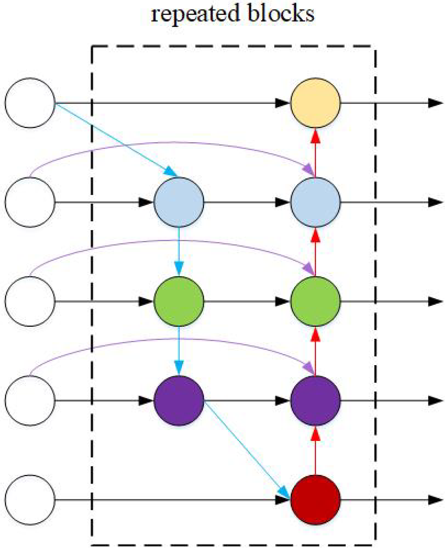
3.3. BiFPN
FPN [
31] stands for feature pyramid networks, which are fundamental components of recognition systems that are used to detect objects at different scales. FPNs connect top-down high-level features with low-level features, which enhances the semantic information of the features at all scales. However, the problem with FPNs is that a limitation regarding unidirectional information flow exists.
BiFPN [
16] is a bidirectional weighted feature pyramid network whose structure is shown in
Figure 7, and it is capable of simply and quickly fusing multiscale features. BiFPN adds cross-scale connections to the network that are not found in other FPNs and removes nodes that only have one input and very little weight in their feature fusion; additionally, it adds skip connections between the input and output nodes so that the output nodes can use both the feature fusion information from the original nodes, as well as the feature information that was feature fused.
The weight differences between the features are usually not considered when fusing the features at different scales via traditional feature fusion, and instead, feature fusion is directly performed. BiFPN uses the weights of features at different scales as parameters for deep learning as well; this feature fusion method is known as fast normalized fusion, and the expression of this fusion method is shown in Equation (
4):
where
and
O denote the features before and after fusion, respectively;
and
denote the weights of the features to be learned; and
is a minimal value that is much smaller than one to ensure the stability of the value.
BiFPN also employs learnable weights that can adaptively adjust the degree of information transfer and fusion, which increases the efficiency of the information utilization and enables the simultaneous up- and downsampling of features without the need to separate the up- and downsampling, as is required for some traditional methods, which prevents computation and memory wastage. Additionally, BiFPN can be used in feature pyramid networks, which enables efficient multiscale feature fusion and can increase the accuracy with which a model performs object-detection tasks through more comprehensive feature interaction and information fusion. The results of experiments on a number of publicly available datasets have shown that models incorporating BiFPN can achieve higher accuracy compared with models without BiFPN. Therefore, YOLO-MBBi uses BiFPN instead of the original feature fusion.
3.4. Enhancements in IoU by Using SIoU
The intersection over union (IoU) is used to calculate the ratio of the intersection and union of the area of two rectangles, the prediction and real box,
and
IoU, as shown in Equation (
5). According to the definition of IoU, the larger the overlapping area of two rectangles, i.e., the intersection, the closer the IoU value is to 1, and vice versa, the closer it is to 0. We generally considered that the prediction could be considered correct when the IoU was greater than a certain threshold value.
To address the problem for objects of different size scales, the enhanced loss functions such as GIoU, DIoU, and CIoU [
13] were optimized based on the original IoU. SIoU [
18] then considers the angle difference between the two rectangular centres of the prediction rectangular on the basis of these IoUs. Note that
is the acute angle between the centres of the two rectangles and can be used to find the angular loss
according to
, as shown in Equations (
6) and (
7). SIoU redefines the distance loss calculation
, which also uses the angle loss function
, as shown in Equations (
8) and (
9):
In addition, SIoU also uses the difference in the similarity of two rectangular shapes as a criterion for calculating the loss function, whereby it defines the shape loss
as shown in Equation (
10), whereby
,
, and
is the hyperparameter. After calculating
and
, the formula for SIoU is provided in Equation (
11):
Compared with the CIoU used in the YOLOv5 network, SIoU redefines the penalty calculation method, considers the vector pinch angle of the desired regression, and calculates more accurate loss values, which is conducive to increasing the accuracy and efficiency of the inference of the regression during training. Therefore, the CIoU loss function used in YOLOv5s is replaced with the SIoU loss function as the locus loss function for the bounding box regression.
3.5. Depth-Wise Convolution
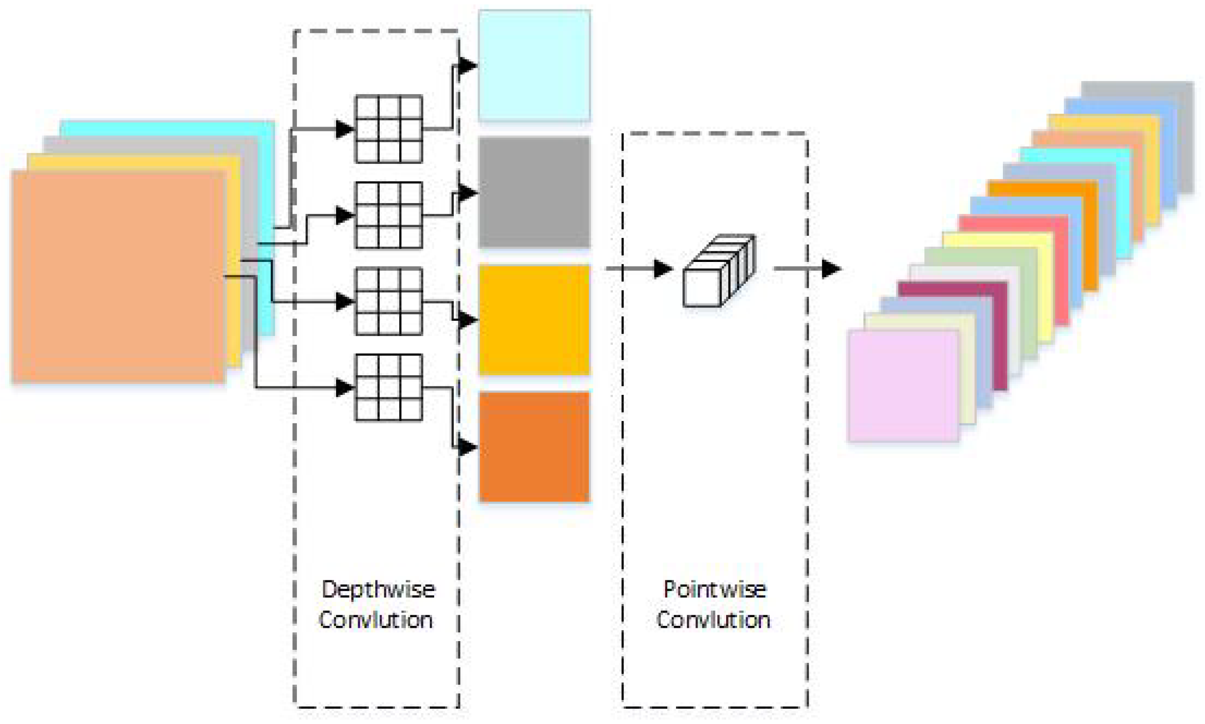
Depth-wise convolution is mainly connected by the depth and point-by-point convolution instead of a separate convolution layer, and its structure is shown in
Figure 8. The depth-wise convolution steps are as follows: firstly, the input feature maps are convolved channel by channel through depth convolution, and the number of channels in the output feature maps is the same as the number of channels in the input feature map; then, point-by-point convolution extends the number of channels in the output feature maps of the previous layer to the final number of channels of the output feature map through the convolution layer of the 1 × 1 convolution kernel.
Depth-wise convolution divides a standard convolutional operation into two suboperations: deep and point-by-point convolution, which thus reduces the number of parameters by nearly 60% and considerably reduces the number of redundant computations. This increases the efficiency and speed of the network by remarkably reducing the number of parameters and the computation amount while maintaining the accuracy of the convolutional neural network. For this experiment, some of the convolutions were replaced with depth-wise convolutions.
4. Experiment Results and Discussion
To verify the effectiveness of YOLO-MBBi at detecting PCB surface defects and the performance enhancement of the enhanced modules for detection, two publicly available datasets called PKU-Market-PCB [
10] and DeepPCB were used to train and determine the performance differences between YOLO-MBBi and Faster-RCNN; additionally, TDD-Net [
10], YOLOv4, YOLOv5s, and YOLOv7 [
32] were compared to verify the superiority of the enhanced model that we propose. Additionally, ablation experiments were conducted to obtain the ablated networks by replacing or deleting the enhanced modules used in the enhanced networks one by one, and the performance of each module was compared with the YOLO-MBBi after the training of these networks was completed to verify the necessity of each module enhancement.
4.1. Experimental Environments
The experimental environment for training and testing was as follows: the deep learning framework was PyTorch1.11.0 + cu113, the CUDA version was 11.1, the operating system was Windows 10, the CPU was i7-11700, the memory size was 32 GB, and the GPU was NVIDIA GeForce RTX 3060 12 G.
4.2. Experiment Dataset
Two PCB surface defect datasets were used for this experiment: PKU-Market-PCB and DeepPCB. Only one dataset was selected for each experiment.
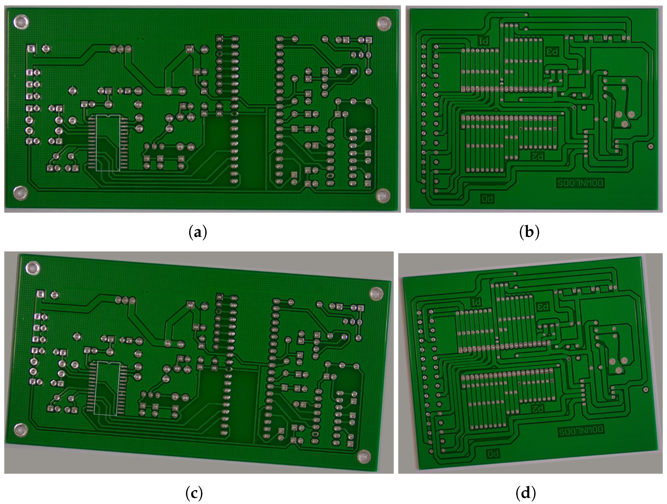
PKU-Market-PCB is a publicly available dataset from Peking University’s Open Laboratory for Intelligent Robotics, and it is a publicly synthesized PCB defect dataset that is labelled with six types of PCB surface defects: missing holes, mouse bites, open circuits, shorts, spurs, and spurious copper. We used 693 images of the normally placed and randomly rotated PCBs for each network. The images of the normally placed PCBs were all captured with an industrial camera with a resolution of 2777 × 2138, as shown in
Figure 9. For this study, all 693 normally placed PCB images were selected, and a further 507 randomly rotated images were selected to form a total dataset of 1200 images for this experiment. We ensured that 200 PCB images containing each defect type were available, and the rotated PCB images were also annotated against the original images to ensure the accuracy of this experiment. The experiments were randomly divided in an 8:1:1 ratio regarding the use of the training, validation, and test set for each of the six defective images. The partition of the dataset is shown in
Table 1.
DeepPCB is a PCB surface defect dataset from GitHub that contains 1500 images of PCBs with six types of surface defects: openings, shorts, mouse bites, spurs, spurious copper, and pinholes. It also contains 1500 corresponding images that do not show defects for comparison and reference purposes. All the images in this dataset were obtained from a linear scan CCD at a resolution of around 48 pixels per 1 millimetre. Each original image had 16k × 16k pixels. These original images were cropped into many sub-images with a size of 640 × 640 and were aligned by using template matching techniques.
Figure 10 displays the normal PCB images and PCB images with surface defects in this dataset. A total of 1200 images were present in the training set, 150 images were present in each of the training and testing sets, and each image showed different types of defects.
Considering the small size of the two datasets chosen, the datasets were randomly divided three times, and each model was trained once on each of the three divided datasets. For each model’s metrics, the average of their corresponding metrics in these three training sessions was taken as the final result.
4.3. Evaluation Metrics
For this study, the mean average precision (mAP), precision, recall, FPS (frame rate of detection), and FLOPs (floating point operations) were used as the evaluation metrics of the model. The precision
P and recall
R for individual category identification were defined as shown in Equation (
12), where
denotes the number of correctly identified object samples,
denotes the number of incorrectly identified object samples, and
denotes the number of unidentified object samples.
Additionally, mAP50 could be calculated according to the recognition accuracy of each category, as shown in Equation (
13). The number 50 reflects the threshold value of the intersection ratio, which is 0.5;
is the total number of items in all the categories; and
is the detection accuracy of the target object in category
i.
The FPS is the number of frames per second and represents the number of images detected per second. The faster the inference rate of the model, the more images are detected per unit of time.
FLOPs refer to the number of floating point operations of a neural network, and it is often used to measure the computational complexity of a neural network, compare the computational efficiency between different neural networks, and evaluate the computational complexity and speed of a model. In general, a higher FLOPs value means that the weight needs to perform more computations and therefore requires more computational resources, and it also means that the model will run slower, although using a model with lower FLOPs can increase the corresponding speed.
4.4. Experiment Results
The Faster-RCNN with ResNet50 as the backbone, TDD-Net [
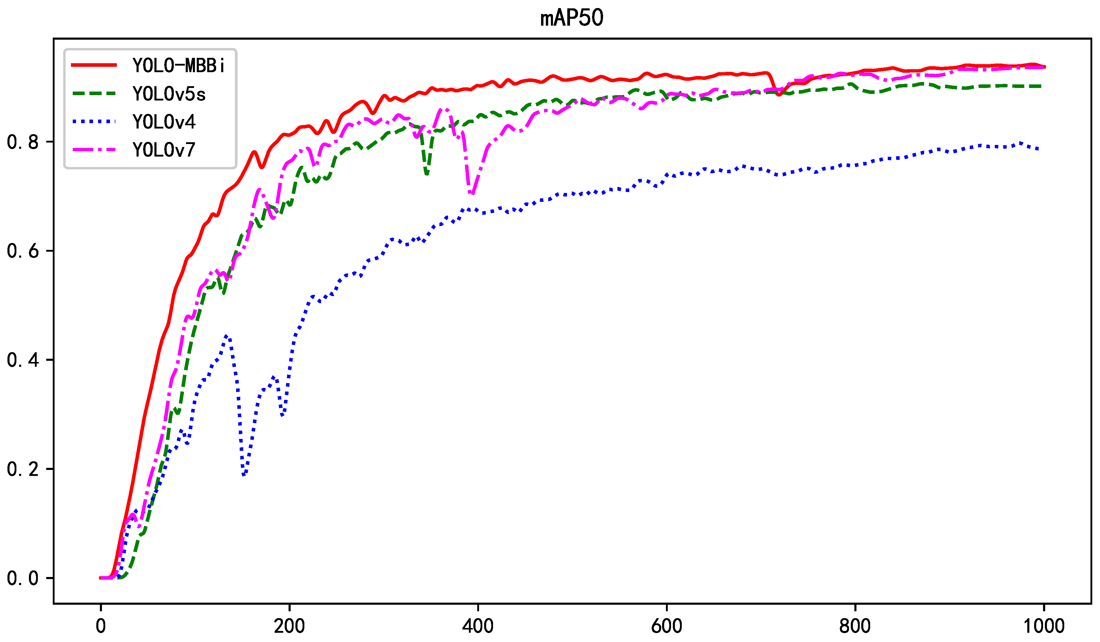
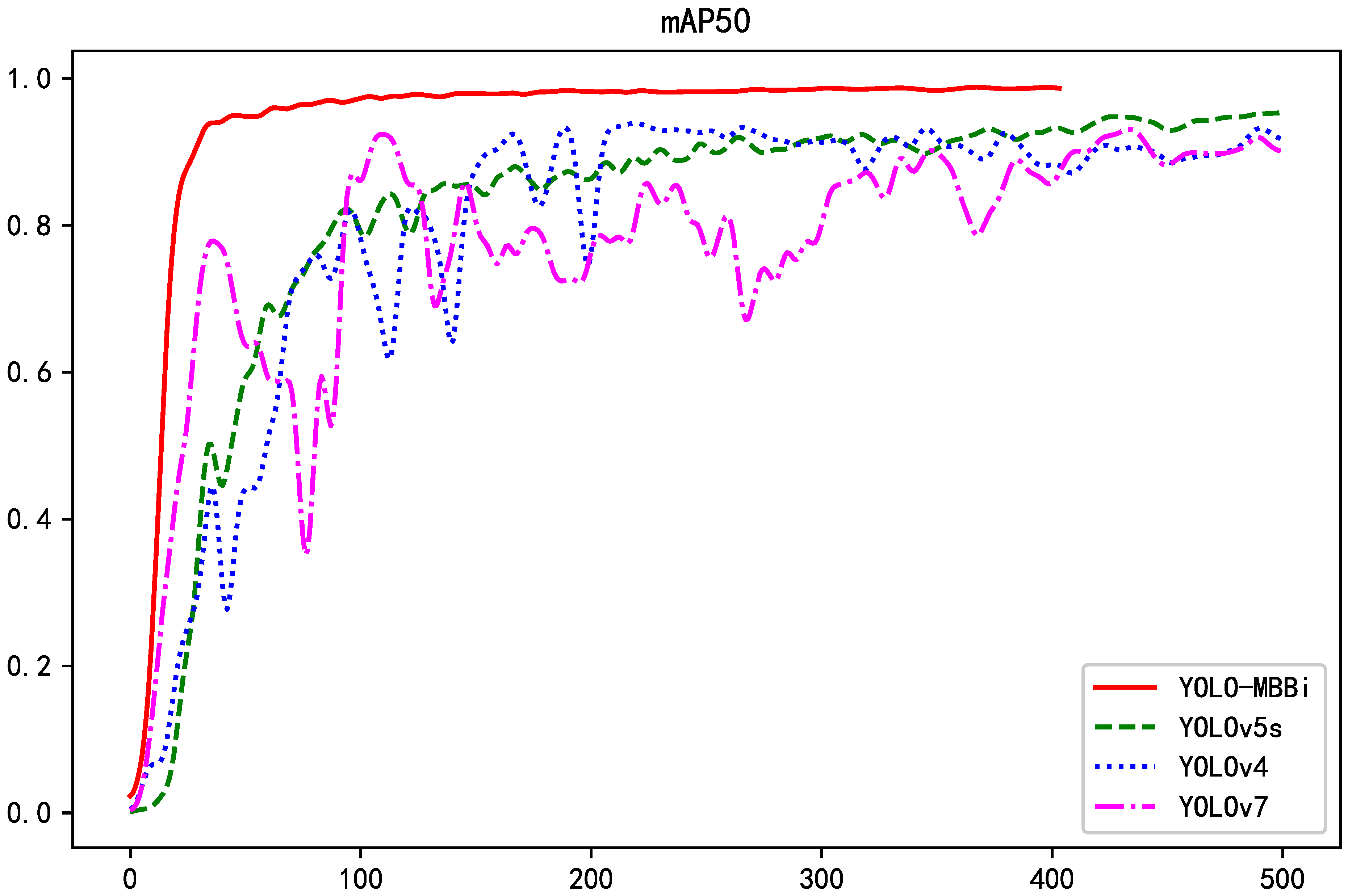
10], YOLOv4, YOLOv5s, YOLOv7, and YOLO-MBBi were selected for the comparison experiments. The training based on the PKU-Market-PCB dataset occurred as follows: The number of training iterations was set to 1000. To ensure that we only use a single variable and to reduce the influence of pretraining weights on the final trained weights, we did not use pretraining weights for any of the weights during the training process. YOLO-MBBi was trained with a batch size of 12, and YOLOv4, YOLOv5s, and YOLOv7 were trained with the default training parameters. Additionally, when training with the DeepPCB dataset, all the conditions remained the same, except that the number of iterations was changed to 500. The changes in mAP50 that occurred when training YOLO-MBBi, YOLOv4, YOLOv5s, and YOLOv7 are plotted in
Figure 11 and
Figure 12, and these weights were evaluated by using the test set; the results of the evaluation are shown in
Table 2 and
Table 3.
Table 4,
Table 5 and
Table 6 show the comparison of the mAP50, precision, and recall obtained when detecting each defect in the PKU-Market-PCB dataset, respectively, and a comparison of the mAP50, precision, and recall obtained when detecting each defect in the DeepPCB dataset can be found in
Table 7,
Table 8 and
Table 9.
As shown in
Figure 11, the growth rate of YOLO-MBBi was faster than that of the other models in the first 600 training sessions. Although the growth rate slowed down in the next 400 training sessions, YOLO-MBBi’s mAP50 values were still close to those of YOLOv7, and in comparison with the original YOLOv5s, its mAP50 grew faster than the original model, and YOLO-MBBi’s final mAP50 values exceeded those of the original model. The test results in
Table 2 show that YOLO-MBBi had the greatest precision of all six weights, with mAP50 values that were consistent with YOLOv7 and 4.6 percentage points higher than that of YOLOv5s. The recall was 1.1 percentage points lower than YOLOv7 but still 2.6 percentage points higher than YOLOv5s. Regarding the model’s complexity, the FLOPs of YOLO-MBBi were only 12.8, which was the lowest computational complexity of all the weights. Additionally, the mAP50 and recall of YOLO-MBBi were close to those of YOLOv7, but the FLOPs were much smaller than those of YOLOv7. Regarding the detection speed, the original YOLOv5s was the highest at 103.1, but YOLO-MBBi achieved an FPS of 48.9, which was still superior compared with the other weights; additionally, it had the smallest computational effort among all six weights, which means that it can be used for PCB industrial inspections.
According to
Figure 12, YOLOv4 and YOLOv7 showed different degrees of overfitting during the training process, whereas the mAP50 value of YOLOv5s grew steadily during the training process. Compared with the other weights, YOLO-MBBi’s mAP50 values steadily and rapidly grew, and its final mAP50 values were much higher than those of the other weights, although training was stopped early at 405 times due to the early stopping mechanism.
Table 3 shows that the newer YOLOv7 did not perform as well with the DeepPCB dataset as it did with the PKU-Market-PCB dataset, whereas the other weights were all enhanced to varying degrees. With this dataset, YOLO-MBBi had higher precision and mAP50 values than the other weights, which reached 98.7 and 99.0%, respectively, and the recall of YOLO-MBBi was slightly lower than that of YOLOv5s, but only by 0.6%. Similarly, YOLO-MBBi did not have the highest detection frame rate when using the DeepPCB dataset, but it still achieved satisfactory values.
For the same metric for each model, the final metric for that model was the average of each category on that metric, and these were mAP50, precision, and recall.
Table 4,
Table 5 and
Table 6 showed that when using the PKU-Market-PCB dataset, YOLO-MBBi and YOLOv5s reached consistent maximum mAP50 values for all the weights, and regarding the four defect types of mouse bites, shorts, spurs, and spurious copper, the YOLO-MBBi mAP50 values were the highest and were the same. Similarly, the precision of YOLO-MBBi when using this dataset was also excellent, as it not only had the highest precision among all the weights but it also had the highest precision for all five defect types: missing holes, mouse bites, open circuits, spurs, and spurious copper. Regarding the recall values, YOLO-MBBi and YOLOv7 both achieved the best results when using this dataset.
Table 7,
Table 8 and
Table 9 show that when using the DeepPCB dataset, YOLO-MBBi achieved the highest mAP50 among all the weights, and YOLO-MBBi had the highest mAP50 values for the five defect types of openings, shorts, mouse bites, spurs, and pinholes. Regarding precision, YOLOv5s achieved the highest precision when using this dataset, but YOLO-MBBi’s precision was only 0.1 percentage points lower, and YOLO-MBBi achieved the highest precision for all four defect types: shorts, mouse bites, spurious copper, and pinholes. Regarding the recall values, YOLO-MBBi achieved the highest recall for openings, mouse bites, spurs, and pinholes, and the average recall was satisfactory. YOLO-MBBi can be considered excellent for detecting different types of PCB surface defects.
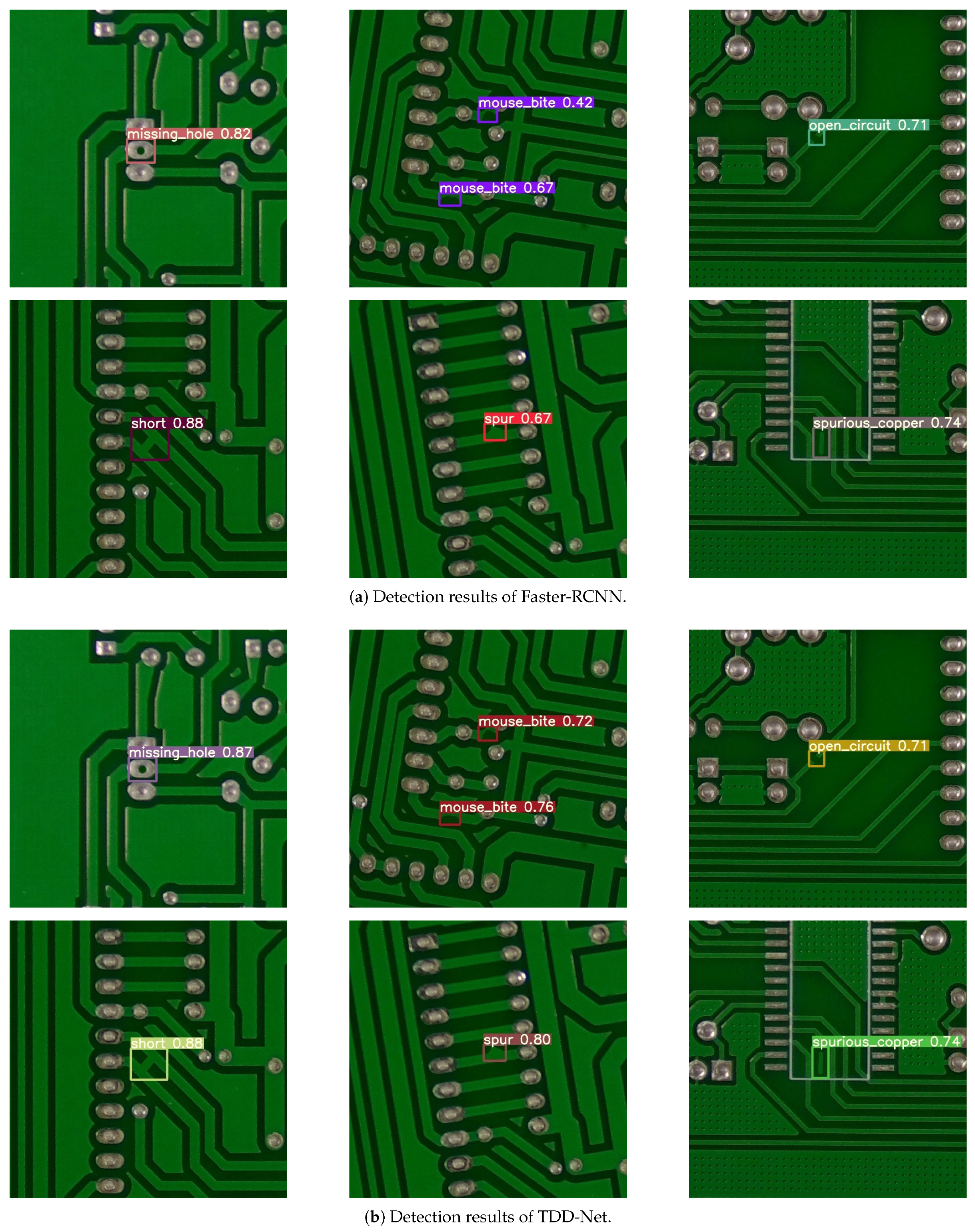
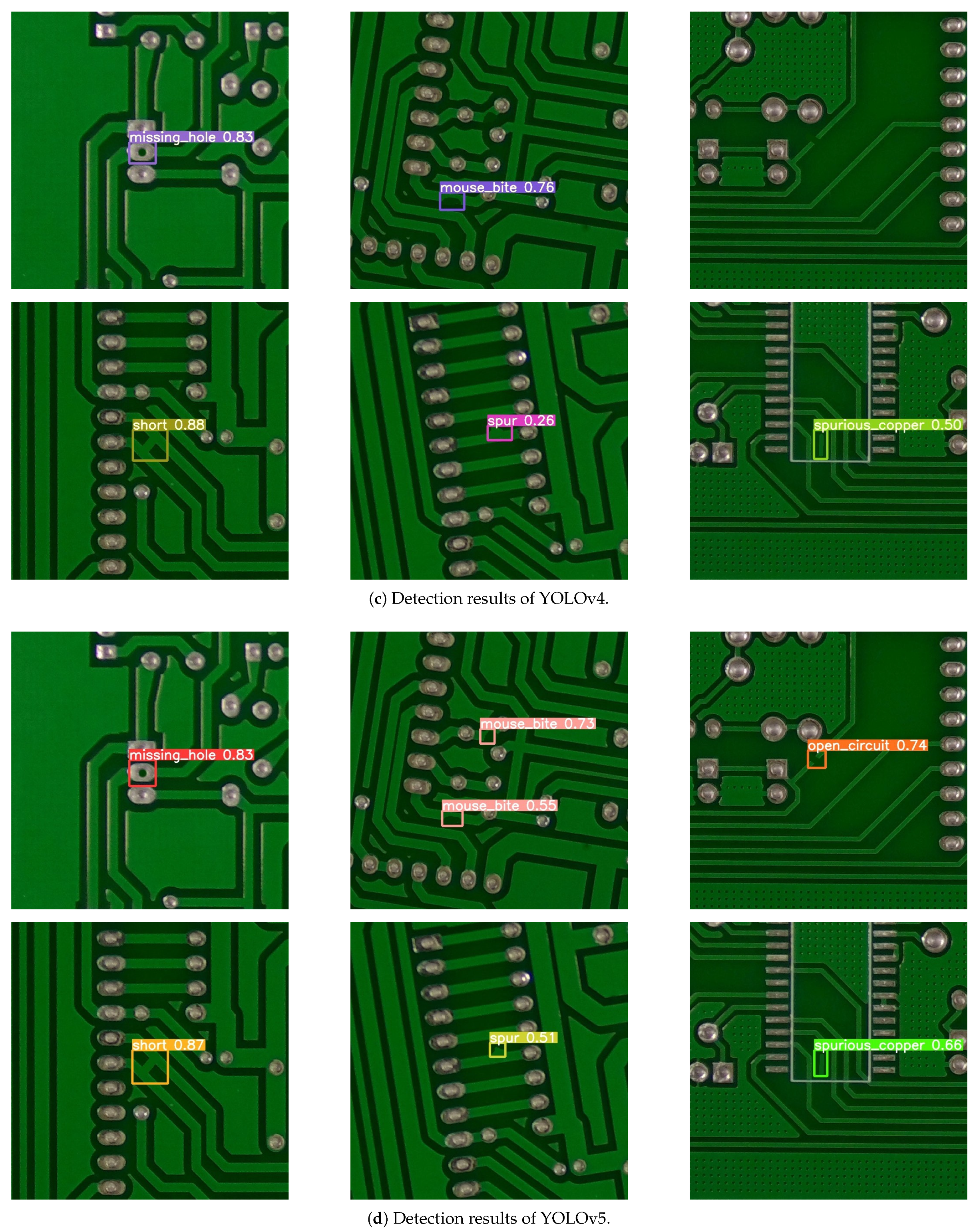
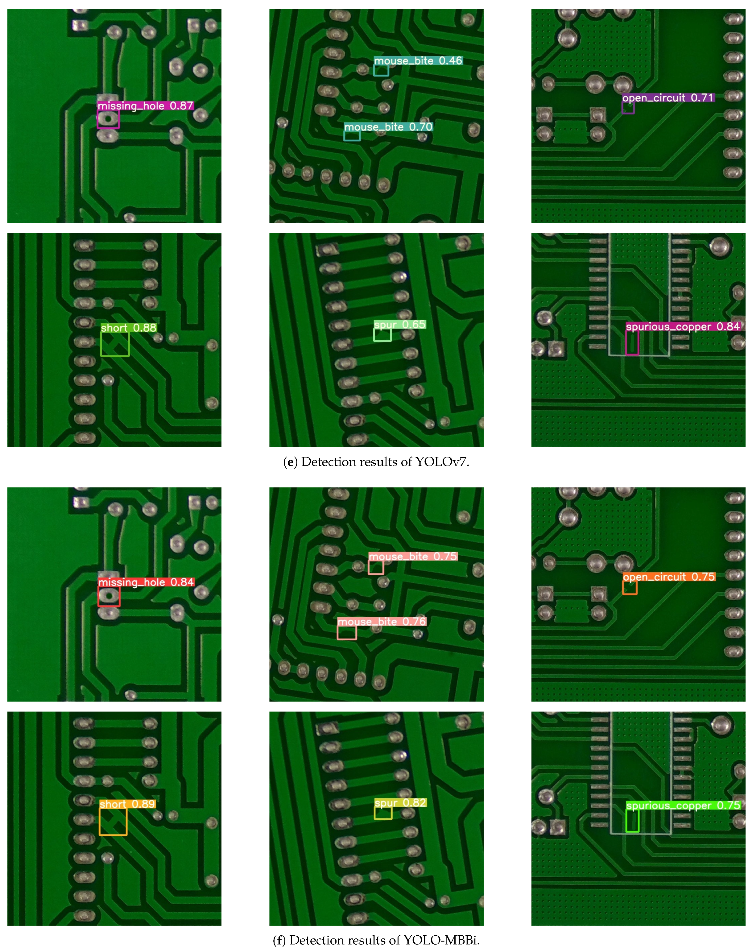
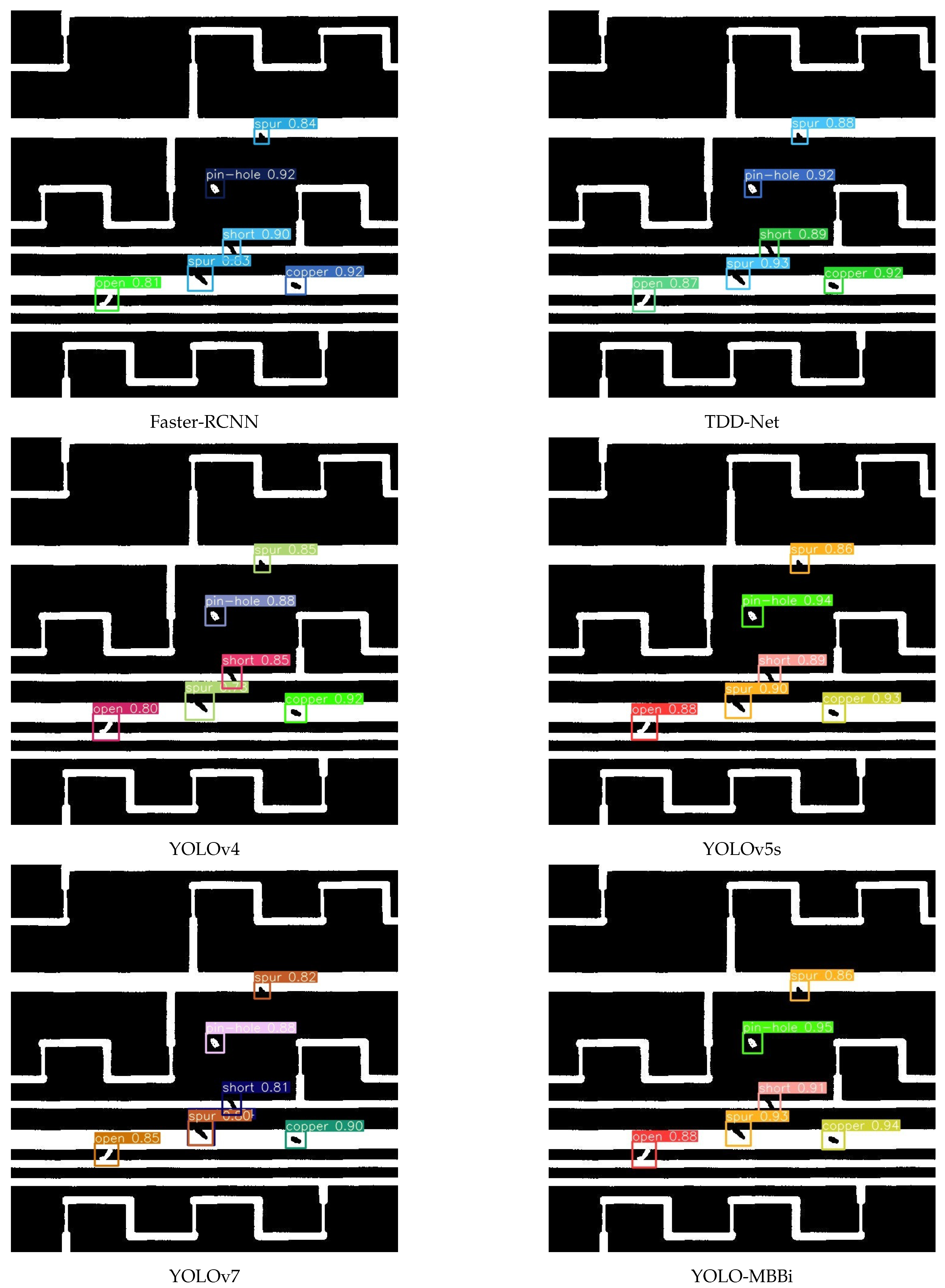
For this study, Faster-RCNN, TDD-Net, YOLOv4, YOLOv5s, YOLOv7, and YOLO-MBBi were each used to detect defects in the test set, and some comparative examples of the detection of these weights are provided in
Figure 13. The comparison results in
Figure 13 show that the results of these weights when identifying and locating PCB defects were generally consistent. Regarding the confidence comparisons, YOLO-MBBi and YOLOv5s had higher confidence when identifying all six surface defects when compared with each other. Compared with YOLOv7, YOLO-MBBi had higher confidence when identifying mouse bites, open circuits, shorts, and spurs and slightly lower confidence when identifying missing holes and spurious copper.
Although the precision of YOLO-MBBi was close to that of the more-advanced YOLOv7, the computational effort of the YOLO-MBBi weights was much less than that of the YOLOv7 weight, and the FPS was also slightly faster than that of YOLOv7. Comparing YOLO-MBBi with the original YOLOv5s, the precision, mAP50 value, and recall were higher than the original YOLOv5s weight. Thus, the YOLO-MBBi is considered superior for PCB surface defect detection. Additionally,
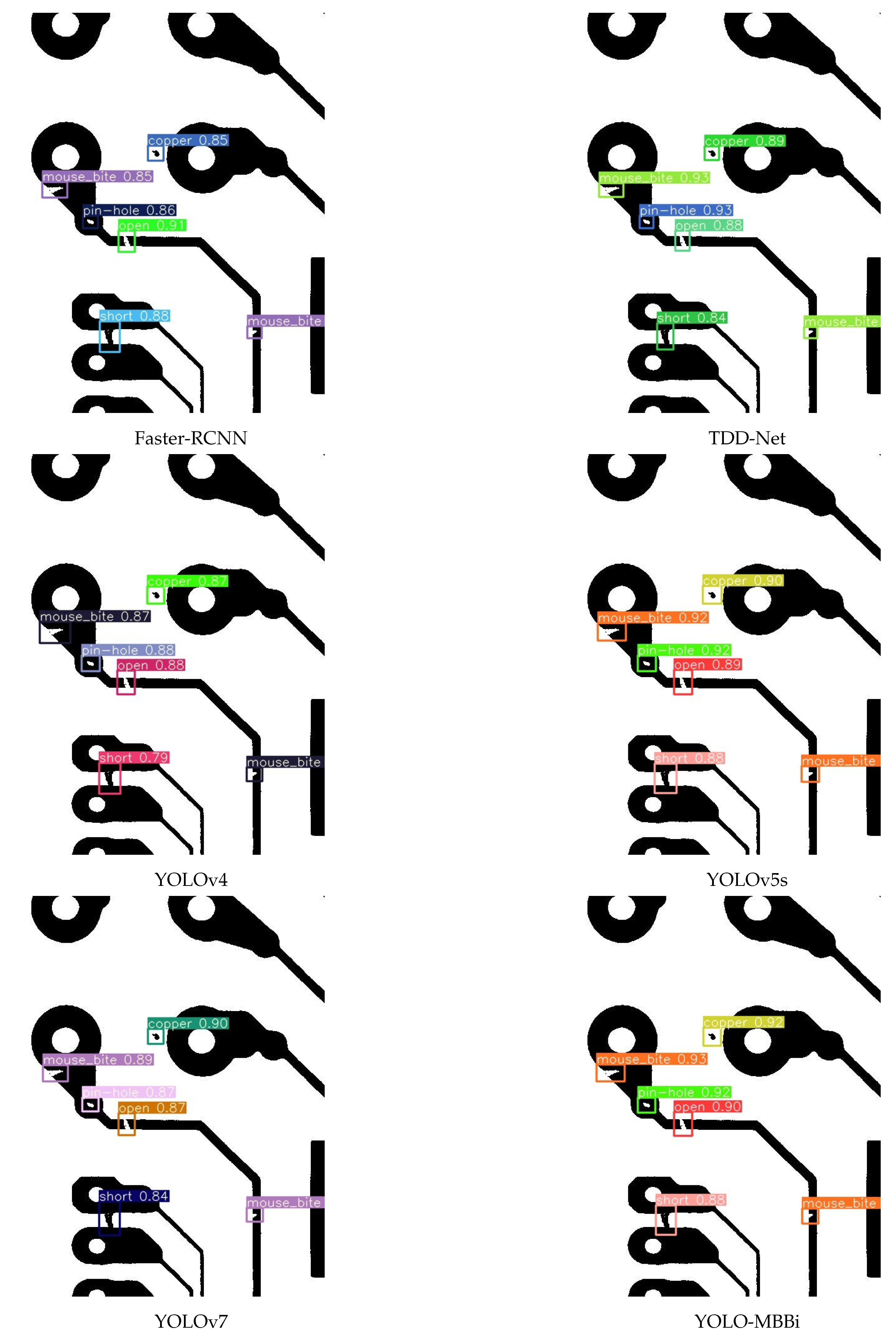
Figure 14 shows that YOLO-MBBi also achieved high confidence levels for each of the detections when using the DeepPCB dataset. From these results, we concluded that YOLO-MBBi can detect PCB surface defects.
4.5. Ablation Experiments
To verify that the MBConv, CBAM, BiFPN, and SIoU, which were used to enhance the YOLOv5s that were previously mentioned, can have a beneficial effect on YOLO-MBBi and to ensure the rigour of the experiments, ablation experiments were conducted for each of these five modules. The experimental scheme was as follows: the CBAM module was removed from the enhanced model to verify the validity of CBAM, and the validity of the remaining modules was verified by replacing the enhanced modules with the original YOLOv5 modules. The results of the ablation experiments are shown in
Table 10 below.
Table 10 shows that the mAP50 value decreased by 3.8 percentage points compared with the YOLO-MBBi when replacing the backbone network with the original version of the convolution and C3 modules, which demonstrates that the backbone network consisting of the MBConv modules had a stronger feature extraction capability than the YOLOv5s backbone network. Removing the CBAM attention had the lowest effect on the decrease in mAP and recall of the network but still demonstrated that CBAM contributed to the performance enhancement of the enhanced network. Additionally, for all the enhanced modules that we propose, the mAP50 values and recall rates decreased to varying degrees when the modules were individually removed or replaced with modules from the original YOLOv5s network, respectively. The results of this ablation experiment demonstrated that each of these enhancement modules had a beneficial impact on the accuracy enhancement of the enhanced YOLOv5s for PCB surface defect detection and that each module was necessary to enhance the network.
5. Conclusions
An enhanced model based on YOLOv5 named YOLO-MBBi is proposed to address the problem of the low accuracy and efficiency of YOLOV5 when detecting surface defects in PCBs. This model uses the faster and more accurate inference mechanism of the MBConv and CBAM attention to replace the backbone network consisting of C3 and normal YOLOv5 convolution and adds BiFPN to the neck network, replaces the ordinary convolution with depth-wise convolution, and changes CIoU to SIoU during training. The experimental results that were obtained after using the public datasets PKU-Market-PCB and DeepPCB demonstrated that the model achieved precision values of 95.8% and 98.7%, which were the highest of all the models used in the experiments. The mAP50 reached 95.3% and 99.0%, which were 3.6% and 1.8% higher than the mAP50 values of the original YOLOv5s, respectively, and the detection FPS reached 48.9 and 69.5, which meets the needs for PCB industrial production.
When conducting subsequent research, we will consider expanding the dataset through data augmentation and the continued optimization of YOLO-MBBi. The main methods used to expand the dataset include using Python scripts to pan, rotate, cut, and stitch the images, as well as adjusting the hue and brightness of the original images by changing the HSV of the images. We will optimize the model by considering lightweighting it for practical applications, deploying the weight on small and microdevices, and conducting experiments in real production line environments so that the model can more efficiently meet the needs of PCB production lines. The optimization weight was mainly considered to lighten the weight, which has practical applications; additionally, the weight was deployed on small microdevices, and it was used to conduct experiments in a real production line environment so that it could more accurately meet the needs of PCB production lines.


