Communication

Near-Infrared CMOS Image Sensors Enabled by Colloidal Quantum Dot-Silicon Heterojunction

Department of Electrical and Computer Engineering, University of Alberta, Edmonton, AB T6G 2V4, Canada
*
Author to whom correspondence should be addressed.
Electronics 2023, 12(12), 2695; https://doi.org/10.3390/electronics12122695
Submission received: 11 May 2023 / Revised: 12 June 2023 / Accepted: 14 June 2023 / Published: 16 June 2023
(This article belongs to the Special Issue Feature Papers in the Optoelectronics Section)

Abstract

:
The solution processibility of colloidal quantum dots (CQDs) promises a straightforward integration with Si readout integrated circuits (Si-ROCIs), which enables a near-infrared (NIR) CMOS image sensor (CIS; CMOS stands for complementary metal-oxide semiconductor). Previously demonstrated CQD NIR CISs were achieved through integrating CQD photodiode or PhotoFET with Si-ROCIs. Here, we conduct a simulation study to investigate the feasibility of a NIR CIS enabled by another integration strategy, that is, by forming a CQD-Si heterojunction. Simulation results clearly show that each active pixel made of CQD-Si heterojunction photodiode on the CIS sensitively responds to NIR light, and generated photocarriers induce changes in electrostatic potentials in the active pixel. The potential changes are read out through the integrated circuits as validated by the readout timing sequence simulation.

1. Introduction

NIR imaging underpins significant applications such as machine vision, factory automation, surveillance, medical imaging, and self-driving cars [1,2]. A mature commercial solution is by using indium gallium arsenide (InGaAs) material [3]. The main process includes high-temperature epitaxial growth of InGaAs on an indium phosphide (InP) substrate, followed by die dicing and flip-chip bonding (or flip-chip hybridization) of InGaAs dies onto Si-based die circuits. However, this method is normally not scalable on wafers which severely limits the throughput. Another drawback is that pixel resolution is fundamentally limited by bond pitch distance during the flip-chip bonding process. For example, InGaAs-based NIR CIS provided by TELEDYNE (Tau® SWIR) has a pixel size of 15 μm and a resolution of 640 × 512 [4]. This is in drastic comparison to Si-based visible CIS, which has a pixel size as small as ~1 μm and a resolution of 3264 × 2448 pixels in an area of just 1 mm × 1 mm in size.
Lead sulfide (PbS) CQDs have received attention for NIR photodetection in recent decades [5,6]. The materials have strong and tunable absorptions in the NIR region, and PbS CQD photodetectors exhibit superior stability compared to the ones made with other CQDs. Numerous works studied and demonstrated PbS CQD photodetectors, with their structures mainly categorized into three types, which are photoconductors [7,8], photodiode [9,10,11,12,13], and photoFET [14,15,16]. Yet, it is challenging to utilize a standalone PbS CQD photodetector for NIR imaging applications. One solution to this issue is by combining CQD photodetectors with a separate mechanical scanning apparatus [17], such as optical lenses; the obvious drawbacks which severely limit real-world applications are that the speed is slow since it is limited by the scanning movement and the setup is bulky. Instead, the other option is to integrate PbS CQD photodetector with a commercial Si-ROIC. Thanks to the solution processability, PbS CQDs can be integrated into a large area on Si-ROICs via simple spin coating, spray, ink printing, etc. [18,19,20]. Thus, CQD-based NIR CIS could be realized with a small pixel size (higher resolution), drastically lower energy budget (without high-temperature processing), and manufacturing complexity (without flip-chip hybridization).
Several PbS CQD NIR CISs have been demonstrated, which were realized by integrating CQD photodiodes [21,22] or photoFET [23] onto ROIC circuits. In 2009, Hayden’s group presented a NIR CIS in which a ternary blend (PbS CQD/P3HT/PCBM) photodiode is integrated with ROICs [21]. The device can detect NIR light up to 1.8 μm, featuring a high EQE of up to 51%. In 2017, Konstantatos and Koppens’ groups proposed to integrate PbS CQD-graphene hybrid photoFET with CMOS ROICs and demonstrated a broadband (300–2000 nm) image sensor. The use of hybrid photoFETs with a detectivity of up to 1012 jones can significantly enhance the sensitivity of the image sensor [23]. In 2022, Tang’s group proposed to integrate an entire PbS CQD photodiode onto bottom Si-based ROICs. The working mechanism is by reading out the photocurrent to the bottom ROIC circuit through a gold bottom electrode. The photodiode design supported fast temporal response and greatly suppressed the noise current; thus, the device rendered a high detectivity value of 2.1 × 10¹² Jones and large 3 dB bandwidth of 140 kHz [22].
Alternatively, forming a CQD-Si heterojunction could be another strategy for integrating CQD with Si-ROICs. Photodetectors enabled by such heterojunctions have been reported, mainly focused on Si surface passivation [24,25,26,27] and device structure engineering [28,29]. Here, we conduct a simulation study and investigate the feasibility of NIR CIS enabled by the formation of CQD-Si heterojunction. Simulation results reveal that photocarriers generated under NIR illumination change electrostatic potential levels in the CQD-Si heterojunction photodiode, which are further read out through external Si-based circuits.

2. Simulation Methods

The simulations were conducted using Taurus Medici. The software is a two-dimensional (2D) device simulator that can model both the electrical and optical characteristics of various semiconductor devices. The structure of one active pixel in the proposed NIR CQD-Si heterojunction CIS is displayed in Figure 1. As can be observed, the architecture resembles the active pixel in a Si-based visible CIS with some extra layers, which are CQD and nickel oxide (NiOx) layers.
The heterojunction is formed between a p-type CQD layer (thickness of 300 nm; doping concentration of 1 × 1016 cm−3) and an n-well Si layer (thickness of 1.0 μm; doping concentration of 1 × 1016 cm−3), which is buried in a p-type (doping concentration of 4 × 1015 cm−3) Si substrate. A pinning layer of NiOx (thickness of 30 nm; doping concentration of 5 × 1019 cm−3) is deposited on top of CQD, which enhances the built-in field of CQD-Si heterojunction. The n-well structure is designed to temporarily store the photocarriers generated from the CQD layer under NIR illumination. Once the transfer gate (TG) is biased (open), the stored photocarriers will transport to a floating diffusion (FD) region made of n+ Si. The accumulation of photocarriers subsequently changes the voltage potential of the FD region, which is monitored by a source follower (SF) transistor, and the information is subsequently transferred to the column bus line through a row-select transistor (RS). A reset transistor (RST) will send a reset signal once it is biased; in this case, both n-well and FD will be reset, and extra charges will be swept out of the pixel. In the simulation, NIR light with a wavelength of 1550 nm was used. Note that since Medici is a 2D simulator, light source power is in the unit of W/cm, in which the third dimension is omitted, and light intensity is in the unit of W/cm2. The same rules apply to other quantities, such as current, which is in the unit of A/cm, and current density is in the unit of A/cm2. To have the highest robustness possible, we referenced material and device parameters from published sources and well-established values. Parameters for CQDs, such as carrier mobility, dielectric constant, absorption coefficient and etc., are all from published experimental data [30,31,32]; parameters for Si are all referenced from the software database. On the other hand, except for basic models (i.e., Poisson, drift-diffusion, and continuity equations), the simulation also utilized other ones for more comprehensive and accurate modeling. For example, AUGER was used to account for Auger recombination in materials, while CONMOB was utilized to model the dependence of carrier mobility on impurity concentrations [33].

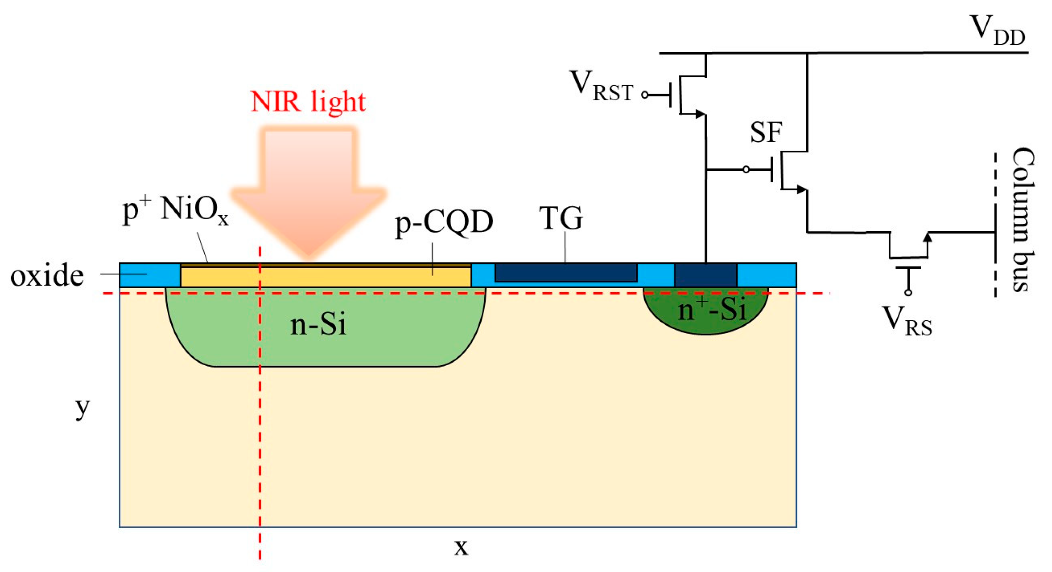
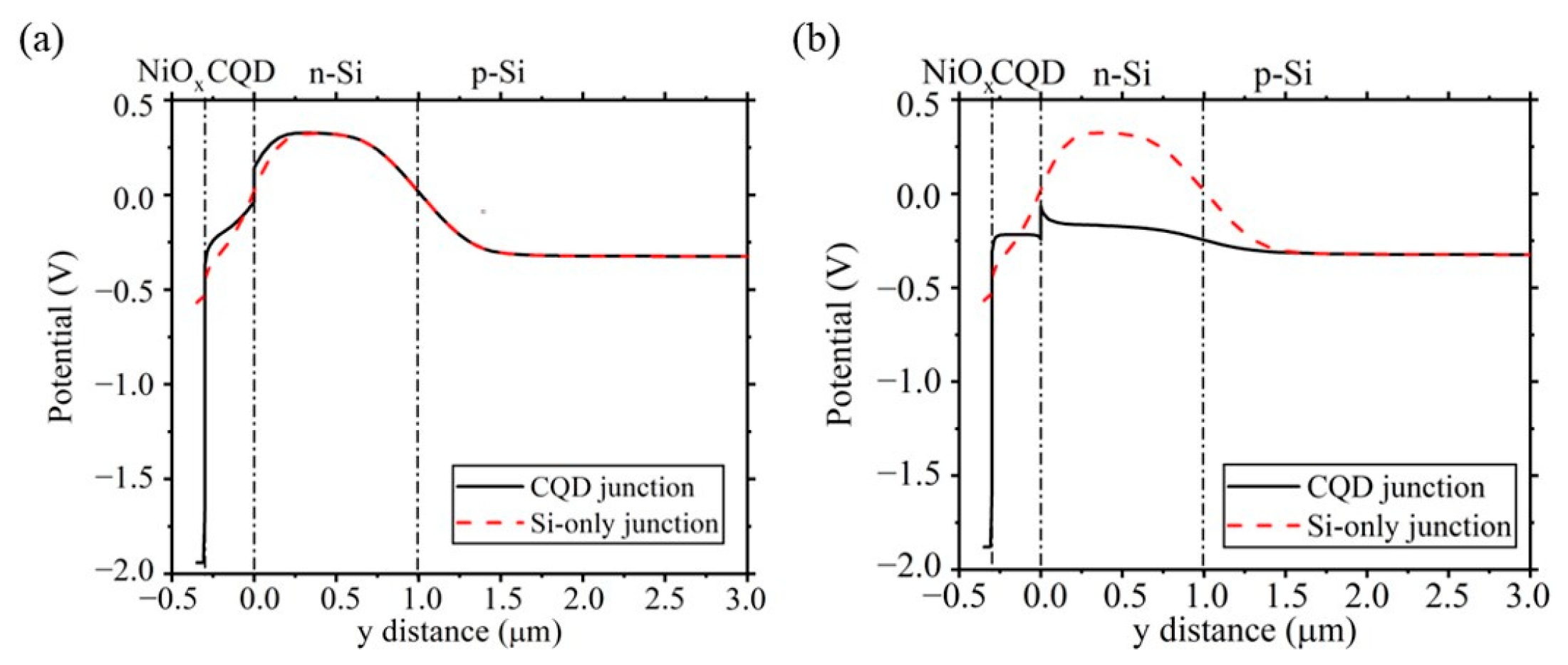
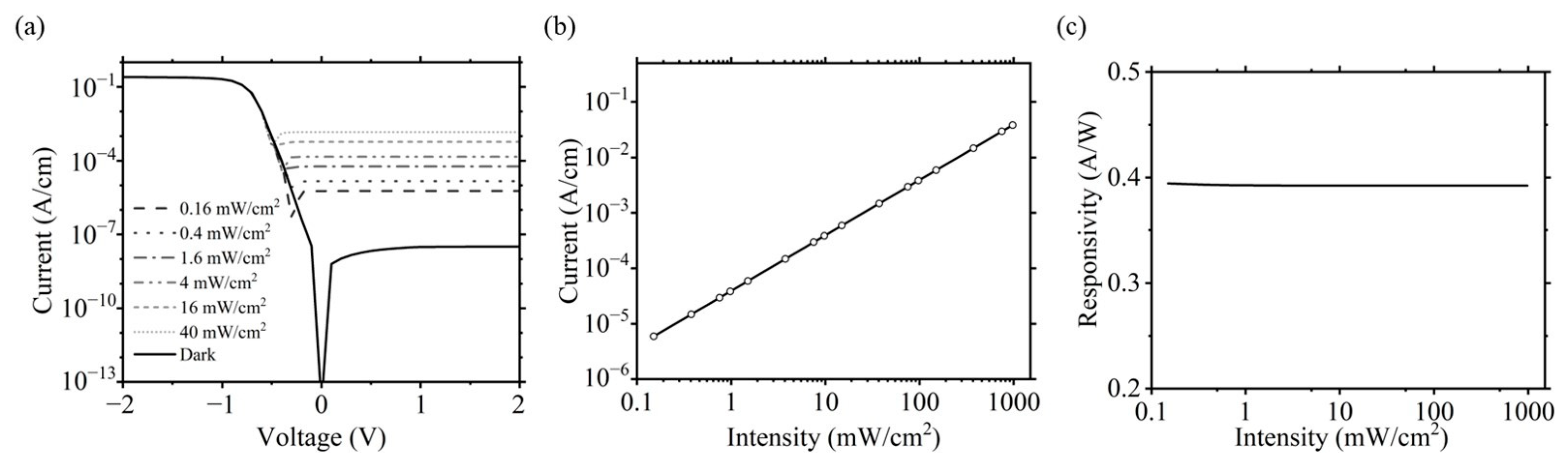
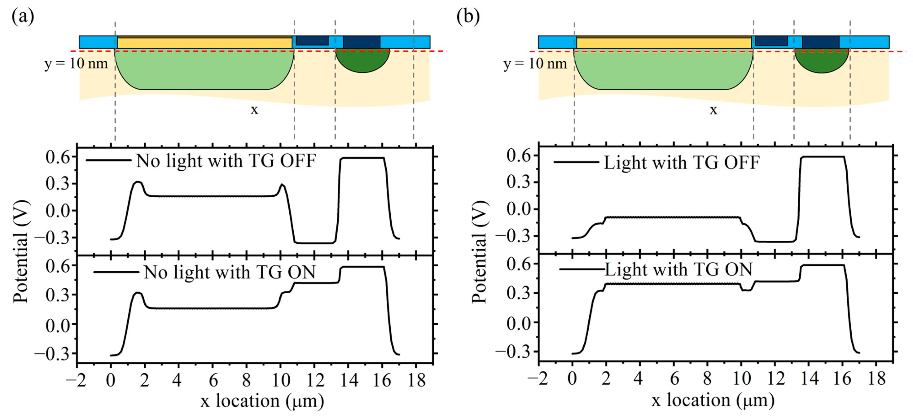
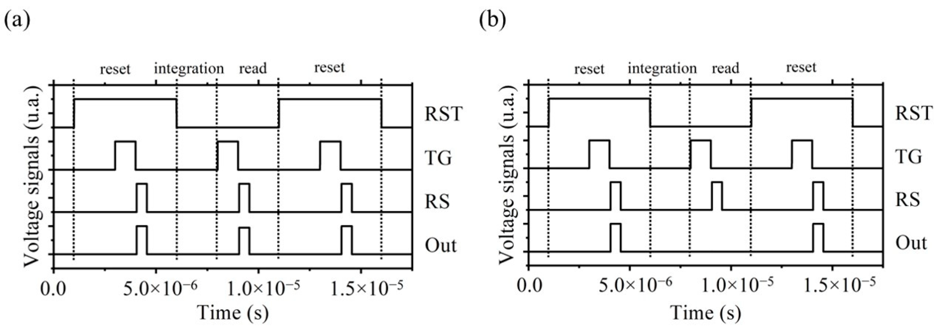
3. Results and Discussion

We first simulate the characteristics of NiOx-CQD-Si heterojunction photodiode that is isolated from the active pixel. Figure 2a,b show the electrostatic potentials (mid-gap potentials) of the structure in the dark and under illumination along the vertical dashed red line shown in Figure 1. Figure 2a shows the potential for a p+/p/n/p type heterojunction formed in the dark. Results reveal that the extra layer of NiOx effectively enhances the built-in electric field, and a potential well for electrons exists in the n-Si region. In Figure 2b and under NIR light illumination, a significant decrease in the voltage potential in the n-well region can be observed; this is because of the accumulation of photo-electrons. Since Si is transparent to 1550 nm light, these photo-electrons are, therefore, generated and transported from the CQD layer. While no significant potential change in the p-Si substrate is observed, the voltage potential in the NiOx layer slightly increases due to the accumulation of holes in the layer. No significant change in electrostatic potential is observed in the p-Si layer because photogenerated holes from the CQD layer will flow directly into NiOx, and therefore, no extra photocarriers will accumulate in this layer.
Figure 3a demonstrates the simulated photocurrent as a function of bias voltage for the photodiode under various light intensities. In the dark, it is observed that a rectifying junction is formed between p-type CQD and n-type Si layers. The photodiode also features low current density down to 3 × 10⁻⁸ A/cm at reverse voltage bias and a high rectification ratio of up to 107. Under NIR light illumination, photocurrent rises with increasing light source power. In Figure 3b, photocurrents as a function of light source intensity are depicted. The values are then fitted using equation Iph ~ Pk, in which k is an empirical number that is closely related to trapping and de-trapping dynamics in the photodiode. From the figure, k is found to be close to 1.0, thanks to the low trap density of the CQD layer [27]. Further, responsivity values are calculated from photocurrent via the equation R = Iph/Pin, where Iph (in A) and Pin (in W) are photocurrents and light source power, respectively. Results are plotted in Figure 3c as a function of light intensity. The values remain stable for all studied light intensities, indicating superior linearity across a wide intensity range, which is crucial for imaging applications. Another figure-of-merit, linear dynamic range (LDR), is used to characterize the linearity of a photodetector. The LDR is defined as LDR = 20 × log (Pmax/Pmin), in which Pmax and Pmin are lower and upper limits for light intensity when the responsivity values start to roll off from linearity. From Figure 3c, the LDR is estimated to be 40 dB for the heterojunction photodiode.
We then proceeded to consider the active pixel in the studied CIS. In Figure 4, we demonstrate the voltage potential calculated along the horizontal direction at y = 10 nm in the dark (Figure 4a) and under illumination (Figure 4b). In both cases, an n-p junction forms horizontally between the n-Si well and the channel beneath the TG gate. When the TG gate is not biased, the n-p junction renders a potential barrier that prevents electrons from traveling through. Once TG is biased, an inversion layer is formed beneath the TG gate and drops the potential barrier. Under illumination (see Figure 4b), photo-generated electrons first transport vertically from the CQD layer and are temporarily stored in the n-well Si if the TG gate is closed, leading to a voltage potential decrease in the n-Si well. Since the results show that the electrostatic potential in the FD region (n+-Si) is higher than in the n-well region (n-Si), the electron carriers will readily transfer horizontally from the n-Si well to the FD region once TG is open.
Finally, we simulate the timing sequence diagram for the entire active pixel as shown in Figure 5. RST, TG, and RS transistors are voltage biased periodically to transfer and read the signal from a selected active pixel to the column bus (see Figure 1). During the simulation, the CIS pixel is exposed to NIR light illumination at all times. A single period can be divided into three stages, which are “reset”, “integration”, and “read”. At the “reset” stage, all three transistors will be biased at VDD, and extra electrons will be cleared out of the pixel. At the “integration” stage, photo-electrons generated in the CQD layer will accumulate (integrate) in the n-well Si region. At the “read” stage, accumulated electrons will further horizontally transport to the FD region once TG is biased, and the signal (voltage potential in the FD region) is read out once RS is biased. After this, the whole process will repeat itself. Within one period (1 × 10⁻⁵ s), it is clear from the figures that the Out signals differ in the dark (Figure 5a) and under illumination (Figure 5b) at the “read” stage: Out remains a high signal level in the dark (no electron accumulation in FD) while it is at a low signal level under NIR light illumination (electron accumulation in FD). The results here prove that CQD-based NIR CIS can generate signals under NIR light using a similar device structure as the conventional Si-based visible CIS.

4. Conclusions

The solution processability of CQDs promises large-area and monolithic integration on Si-ROICs; this enables low-cost CQD-based NIR CIS with high resolution. This report presented a simulation study on CQD-based CIS, in which CQDs were integrated by forming a CQD-Si heterojunction. We first simulated the characteristics of a CQD-Si heterojunction photodiode that was isolated from the CIS active pixel, including dark current, responsivity, and LDR values. Results showed that CIS was sensitive to NIR light with a wavelength of 1550 nm thanks to CQD film. We then demonstrated the working mechanisms by calculating electrostatic potentials in the active pixel. Finally, through a timing sequence simulation, we proved that signals were successfully transferred to the column bus through the ROICs. The investigation in this work provides an alternative integration method of CQDs with Si ROICs for achieving CQD-based NIR CIS.

Author Contributions

Conceptualization, Q.X. and X.W.; methodology, Q.X., X.T., J.Z. and X.W.; software, X.T.; validation, Q.X., X.T. and X.W.; formal analysis, Q.X., X.T., J.Z. and X.W.; investigation, Q.X., X.T., J.Z. and X.W.; resources, Q.X., X.T., J.Z. and X.W.; data curation, Q.X., X.T., J.Z. and X.W.; writing—original draft preparation, Q.X.; writing—review and editing, Q.X. and X.W.; visualization, Q.X.; supervision, X.W.; project administration, X.W.; funding acquisition, X.W. All authors have read and agreed to the published version of the manuscript.

Funding

This research was funded by the Natural Sciences and Engineering Research Council of Canada (NSERC Discovery Grant program; RGPIN-2019-04664). Q.X. acknowledges Alberta Innovates Graduate Student Scholarship (GSS) and Killam Trust—Izaak Walton Killam Memorial Scholarship. X.T. acknowledges Mitacs Globalink.

Data Availability Statement

Data is available from authors upon request.

Conflicts of Interest

The authors declare no conflict of interest. The funders had no role in the design of the study; in the collection, analyses, or interpretation of data; in the writing of the manuscript; or in the decision to publish the results.

References

  1. Afara, I.O.; Shaikh, R.; Nippolainen, E.; Querido, W.; Torniainen, J.; Sarin, J.K.; Kandel, S.; Pleshko, N.; Töyräs, J. Characterization of Connective Tissues Using Near-Infrared Spectroscopy and Imaging. Nat. Protoc. 2021, 16, 1297–1329. [Google Scholar] [CrossRef] [PubMed]
  2. Luo, Y.; Remillard, J.; Hoetzer, D. Pedestrian Detection in Near-Infrared Night Vision System. In Proceedings of the IEEE Intelligent Vehicles Symposium, La Jolla, CA, USA, 21–24 June 2010. [Google Scholar]
  3. Manda, S.; Matsumoto, R.; Saito, S.; Maruyama, S.; Minari, H.; Hirano, T.; Takachi, T.; Fujii, N.; Yamamoto, Y.; Zaizen, Y.; et al. High-Definition Visible-SWIR InGaAs Image Sensor Using Cu-Cu Bonding of III-V to Silicon Wafer. In Proceedings of the 2019 IEEE International Electron Devices Meeting (IEDM), San Francisco, CA, USA, 7–11 December 2019; pp. 16.7.1–16.7.4. [Google Scholar]
  4. Teledyne FLIR Tau® SWIR. Available online: https://www.flir.com/support/products/tau-swir/#Overview (accessed on 1 May 2023).
  5. García de Arquer, F.P.; Armin, A.; Meredith, P.; Sargent, E.H. Solution-Processed Semiconductors for next-Generation Photodetectors. Nat. Rev. Mater. 2017, 2, 16100. [Google Scholar] [CrossRef] [Green Version]
  6. Meng, L.; Wang, X. Doping Colloidal Quantum Dot Materials and Devices for Photovoltaics. Energies 2022, 15, 2458. [Google Scholar] [CrossRef]
  7. Konstantatos, G.; Howard, I.; Fischer, A.; Hoogland, S.; Clifford, J.; Klem, E.; Levina, L.; Sargent, E.H. Ultrasensitive Solution-Cast Quantum Dot Photodetectors. Nature 2006, 442, 180–183. [Google Scholar] [CrossRef] [PubMed]
  8. He, J.; Qiao, K.; Gao, L.; Song, H.; Hu, L.; Jiang, S.; Zhong, J.; Tang, J. Synergetic Effect of Silver Nanocrystals Applied in PbS Colloidal Quantum Dots for High-Performance Infrared Photodetectors. ACS Photonics 2014, 1, 936–943. [Google Scholar] [CrossRef]
  9. Clifford, J.P.; Konstantatos, G.; Johnston, K.W.; Hoogland, S.; Levina, L.; Sargent, E.H. Fast, Sensitive and Spectrally Tuneable Colloidal-Quantum-Dot Photodetectors. Nat. Nanotechnol. 2009, 4, 40–44. [Google Scholar] [CrossRef]
  10. Pal, B.N.; Robel, I.; Mohite, A.; Laocharoensuk, R.; Werder, D.J.; Klimov, V.I. High-Sensitivity p-n Junction Photodiodes Based on PbS Nanocrystal Quantum Dots. Adv. Funct. Mater. 2012, 22, 1741–1748. [Google Scholar] [CrossRef]
  11. Manders, J.R.; Lai, T.-H.; An, Y.; Xu, W.; Lee, J.; Kim, D.Y.; Bosman, G.; So, F. Low-Noise Multispectral Photodetectors Made from All Solution-Processed Inorganic Semiconductors. Adv. Funct. Mater. 2014, 24, 7205–7210. [Google Scholar] [CrossRef]
  12. Jarzab, D.; Szendrei, K.; Yarema, M.; Pichler, S.; Heiss, W.; Loi, M.A. Charge-Separation Dynamics in Inorganic-Organic Ternary Blends for Efficient Infrared Photodiodes. Adv. Funct. Mater. 2011, 21, 1988–1992. [Google Scholar] [CrossRef] [Green Version]
  13. Lee, J.W.; Kim, D.Y.; So, F. Unraveling the Gain Mechanism in High Performance Solution-Processed PbS Infrared PIN Photodiodes. Adv. Funct. Mater. 2015, 25, 1233–1238. [Google Scholar] [CrossRef]
  14. Konstantatos, G.; Badioli, M.; Gaudreau, L.; Osmond, J.; Bernechea, M.; de Arquer, F.P.G.; Gatti, F.; Koppens, F.H.L. Hybrid Graphene–Quantum Dot Phototransistors with Ultrahigh Gain. Nat. Nanotechnol. 2012, 7, 363–368. [Google Scholar] [CrossRef] [PubMed]
  15. Nikitskiy, I.; Goossens, S.; Kufer, D.; Lasanta, T.; Navickaite, G.; Koppens, F.H.L.; Konstantatos, G. Integrating an Electrically Active Colloidal Quantum Dot Photodiode with a Graphene Phototransistor. Nat. Commun. 2016, 7, 11954. [Google Scholar] [CrossRef] [PubMed] [Green Version]
  16. Adinolfi, V.; Sargent, E.H. Photovoltage Field-Effect Transistors. Nature 2017, 542, 324–327. [Google Scholar] [CrossRef] [PubMed]
  17. Tang, X.; Ackerman, M.M.; Guyot-Sionnest, P. Thermal Imaging with Plasmon Resonance Enhanced HgTe Colloidal Quantum Dot Photovoltaic Devices. ACS Nano 2018, 12, 7362–7370. [Google Scholar] [CrossRef] [PubMed]
  18. Li, M.; Zhang, W.; Shao, G.; Kan, H.; Song, Z.; Xu, S.; Yu, H.; Jiang, S.; Luo, J.; Liu, H. Sensitive NO 2 Gas Sensors Employing Spray-Coated Colloidal Quantum Dots. Thin Solid Films 2016, 618, 271–276. [Google Scholar] [CrossRef]
  19. Kramer, I.J.; Minor, J.C.; Moreno-Bautista, G.; Rollny, L.; Kanjanaboos, P.; Kopilovic, D.; Thon, S.M.; Carey, G.H.; Chou, K.W.; Zhitomirsky, D.; et al. Efficient Spray-Coated Colloidal Quantum Dot Solar Cells. Adv. Mater. 2015, 27, 116–121. [Google Scholar] [CrossRef] [Green Version]
  20. Sliz, R.; Lejay, M.; Fan, J.Z.; Choi, M.-J.; Kinge, S.; Hoogland, S.; Fabritius, T.; García de Arquer, F.P.; Sargent, E.H. Stable Colloidal Quantum Dot Inks Enable Inkjet-Printed High-Sensitivity Infrared Photodetectors. ACS Nano 2019, 13, 11988–11995. [Google Scholar] [CrossRef]
  21. Rauch, T.; Böberl, M.; Tedde, S.F.; Fürst, J.; Kovalenko, M.V.; Hesser, G.; Lemmer, U.; Heiss, W.; Hayden, O. Near-Infrared Imaging with Quantum-Dot-Sensitized Organic Photodiodes. Nat. Photonics 2009, 3, 332–336. [Google Scholar] [CrossRef]
  22. Liu, J.; Liu, P.; Chen, D.; Shi, T.; Qu, X.; Chen, L.; Wu, T.; Ke, J.; Xiong, K.; Li, M.; et al. A Near-Infrared Colloidal Quantum Dot Imager with Monolithically Integrated Readout Circuitry. Nat. Electron. 2022, 5, 443–451. [Google Scholar] [CrossRef]
  23. Goossens, S.; Navickaite, G.; Monasterio, C.; Gupta, S.; Piqueras, J.J.; Pérez, R.; Burwell, G.; Nikitskiy, I.; Lasanta, T.; Galán, T.; et al. Broadband Image Sensor Array Based on Graphene–CMOS Integration. Nat. Photonics 2017, 11, 366–371. [Google Scholar] [CrossRef] [Green Version]
  24. Masala, S.; Adinolfi, V.; Sun, J.-P.; Del Gobbo, S.; Voznyy, O.; Kramer, I.J.; Hill, I.G.; Sargent, E.H. The Silicon:Colloidal Quantum Dot Heterojunction. Adv. Mater. 2015, 27, 7445–7450. [Google Scholar] [CrossRef]
  25. Xiao, X.; Xu, K.; Yin, M.; Qiu, Y.; Zhou, W.; Zheng, L.; Cheng, X.; Yu, Y.; Ning, Z. High Quality Silicon: Colloidal Quantum Dot Heterojunction Based Infrared Photodetector. Appl. Phys. Lett. 2020, 116, 101102. [Google Scholar] [CrossRef]
  26. Xu, Q.; Cheong, I.T.; Meng, L.; Veinot, J.G.C.; Wang, X. Silicon Surface Passivation for Silicon-Colloidal Quantum Dot Heterojunction Photodetectors. ACS Nano 2021, 15, 18429–18436. [Google Scholar] [CrossRef] [PubMed]
  27. Xu, Q.; Cheong, I.T.; Song, H.; Van, V.; Veinot, J.G.C.; Wang, X. Heterogeneous Integration of Colloidal Quantum Dot Inks on Silicon Enables Highly Efficient and Stable Infrared Photodetectors. ACS Photonics 2022, 9, 2792–2801. [Google Scholar] [CrossRef]
  28. Xu, K.; Xiao, X.; Zhou, W.; Jiang, X.; Wei, Q.; Chen, H.; Deng, Z.; Huang, J.; Chen, B.; Ning, Z. Inverted Si:PbS Colloidal Quantum Dot Heterojunction-Based Infrared Photodetector. ACS Appl. Mater. Interfaces 2020, 12, 15414–15421. [Google Scholar] [CrossRef] [PubMed]
  29. Zhou, W.; Zheng, L.; Ning, Z.; Cheng, X.; Wang, F.; Xu, K.; Xu, R.; Liu, Z.; Luo, M.; Hu, W.; et al. Silicon: Quantum Dot Photovoltage Triodes. Nat. Commun. 2021, 12, 6696. [Google Scholar] [CrossRef] [PubMed]
  30. Xu, Q.; Meng, L.; Sinha, K.; Chowdhury, F.I.; Hu, J.; Wang, X. Ultrafast Colloidal Quantum Dot Infrared Photodiode. ACS Photonics 2020, 7, 1297–1303. [Google Scholar] [CrossRef]
  31. Lan, X.; Voznyy, O.; Kiani, A.; García De Arquer, F.P.; Abbas, A.S.; Kim, G.H.; Liu, M.; Yang, Z.; Walters, G.; Xu, J.; et al. Passivation Using Molecular Halides Increases Quantum Dot Solar Cell Performance. Adv. Mater. 2016, 28, 299–304. [Google Scholar] [CrossRef]
  32. Aqoma, H.; Al Mubarok, M.; Hadmojo, W.T.; Lee, E.H.; Kim, T.W.; Ahn, T.K.; Oh, S.H.; Jang, S.Y. High-Efficiency Photovoltaic Devices Using Trap-Controlled Quantum-Dot Ink Prepared via Phase-Transfer Exchange. Adv. Mater. 2017, 29, 1605756. [Google Scholar] [CrossRef]
  33. Medici Manual. Available online: https://dunham.ece.uw.edu/ee531/Winter05/MD_2002.4.pdf (accessed on 9 June 2023).
Figure 1. Schematics of an active pixel of a CQD-based NIR CIS.
Electronics 12 02695 g001
Figure 2. Electrostatic potential of NiOx/CQD/Si and Si-only heterojunction photodiodes in (a) dark and (b) under illumination along the red dashed line shown in Figure 1. Light intensity is 13 W/cm2.
Electronics 12 02695 g002
Figure 3. (a) I-V curves of NiO/CQD/Si heterojunction photodiode in the dark and various light intensities. (b) Photocurrent at various intensities. (c) Responsivity values as a function of intensity showing good linearity.
Electronics 12 02695 g003
Figure 4. Electrostatic potential of the active pixel along the horizontal red dashed line in Figure 1 (y = 10 nm) in (a) dark and (b) under illumination. Light intensity is 13 W/cm2.
Electronics 12 02695 g004
Figure 5. Timing sequence diagram of the active pixel (a) in the dark and (b) under illumination.
Electronics 12 02695 g005
Disclaimer/Publisher’s Note: The statements, opinions and data contained in all publications are solely those of the individual author(s) and contributor(s) and not of MDPI and/or the editor(s). MDPI and/or the editor(s) disclaim responsibility for any injury to people or property resulting from any ideas, methods, instructions or products referred to in the content.

