1. Introduction
The growing demand for advanced precision medicine to manage chronic diseases, such as diabetes [
1,
2,
3,
4], glaucoma [
5], gastro-esophageal reflux [
6], epilepsy [
7], Alzheimer’s disease [
8], etc., presents promising opportunities for implantable biosensor microsystems. For the individualized treatment of these diseases, biosensors must collect comprehensive datasets that are well coupled with patients’ daily activities and dietary habits over a long period of time [
9]. However, in most previously published studies, biosensor systems either take a one-point–one-time approach to sensing biosignals or cause discomfort to patients due to continuous monitoring.
For example, some diabetic biosensor systems use implanted glucose sensors with RFID tags [
1,
2,
3,
4] that can retrieve data only when magnetically powered by an external reader. These types of approach do not track transient excursions of the indicator, and thus fail to provide reliable glucose dynamics over time. In other studies, [
10,
11] a battery-powered reader is externally attached to a patient’s skin such that measured glucose concentration can be collected from an implanted passive circuit. However, the externally attached reader often causes inconvenience to patients and skin inflammations in long-term use [
12].
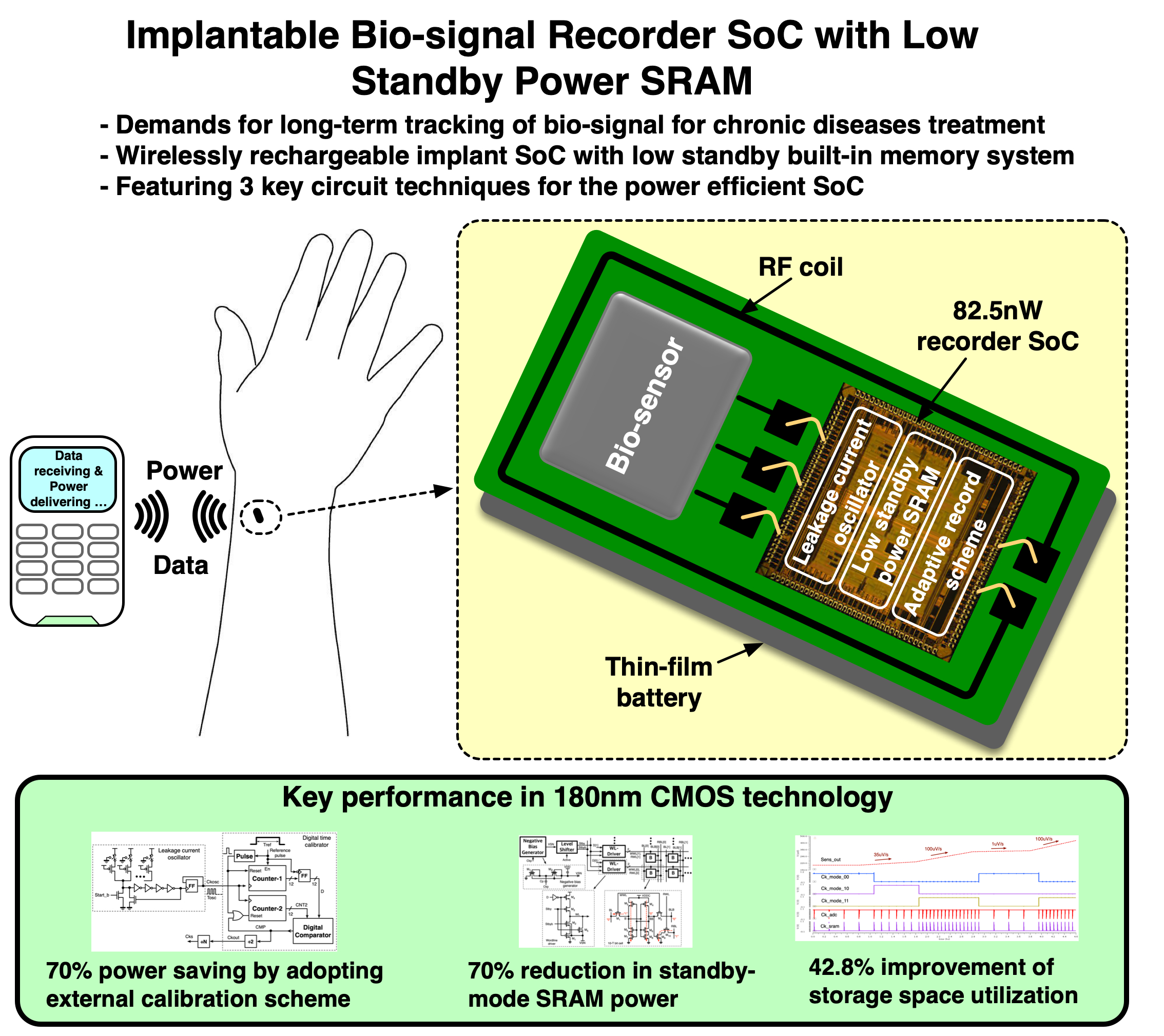
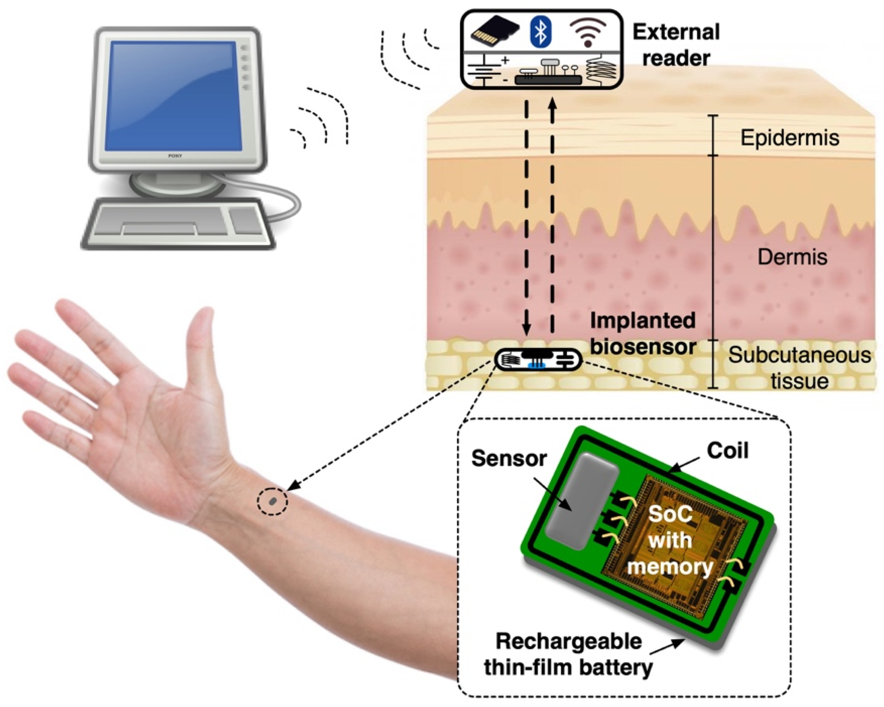
For the purpose of managing chronic diseases or taking preventative measures against such diseases, the continuous tracking of biomarker variations over a significant time period is indispensable [
13]. An implantable biosensor SoC (
Figure 1) that has a rechargeable battery and internal storage space and can be injected with a syringe [
14] or minor subcutaneous surgery [
11] serves this purpose. Therefore, once the battery is charged wirelessly from an external reader, the implant performs sensing and collecting operations while consuming battery power. During the next charging event, the stored datasets are retrieved by the external reader while the internal battery is recharged.
For this type of approach, there are several challenges to tackle. One of the major challenges is that the power budget is extremely limited, given that only tiny size rechargeable batteries are feasible for use in implants. Especially under a very low duty-cycled (<<0.1%) operation, standby power consumption becomes crucial. The other challenge is that the power consumption of internal memory can be significant, directly relying on the size of cell arrays. This implies that there is an inevitable tradeoff between comprehensiveness of collected data and storage space.
In the proposed biosensor system, as shown in
Figure 2, one of the components with a large power dissipation during the standby (or sensing) mode is the clock generator. A leakage-current oscillator is a good candidate for this purpose. However, its high sensitivity to processing and temperature variations often require a periodic correction scheme to adjust the oscillation period referenced by an additional RC-based oscillator, [
12] which consumes significant power. In this paper, we propose a new calibration scheme that utilizes an externally provided reference pulse in order to eliminate the need for internal reference. Another source of large power dissipation can be caused by leakage current from large arrays of memory cells. The total cell leakage power becomes especially significant in standby mode as the memory array size increases. To maintain extremely low quiescent bit-cell current in the standby state, an 8Kbit SRAM based on 10 T cells with a negative wordline and dynamic supply voltage scheme was investigated in this study.
The frequency of sampling at the sensor frontend actually determines the size of digitized datasets to be recorded in the memory. As for the improved efficiency of the storage space, the sampling frequency needs to be synchronized with the rate of incoming bio-signal variations. In other words, when the fluctuation of the input bio-signal increases, the period of sensing needs to be adaptively reduced to record details of signal variation. Additionally, when the input signal variation is insignificant, the sensing period can be extended to save power and storage space. For this purpose, this paper presents an adaptive sensing scheme to minimize the size of internal memory without losing the significant movement of bio-signals.
The safety and reliability of these biosensors embedded in human tissue for long periods of time is an important issue. This is because chemical contamination from electronics into body tissues may cause foreign body reactions (FBRs) and tissue inflammation. Conversely, various ions (especially Na
+) in body fluids may affect the reliability of implanted devices during long-term use [
15]. However, there have been many active studies on these issues to develop biocompatible encapsulation substances, such as Parylene-C [
16] and packaging technologies [
17], in order to isolate electronic devices from surrounding biological fluids and tissues. Recently, the possibility of the unlimited use of biosensors embedded in subcutaneous tissue [
11] has also been reported. Therefore, we believe that the proposed approach of long-term monitoring is a feasible solution.
The method of strategic development of this study aims to prove the effectiveness of the proposed circuit techniques and schemes via comparative studies. In this purpose, the previously studied biosensor SoC [
12] in a smart contact lens system has been selected for comparison. Although this existing SoC does not have data storage and a battery system, it is still useful for comparing and estimating overhead due to its additionally proposed functionalities. The main targets of systematic comparison will be the estimation of additional power overhead due to 8 Kbit-size SRAM with a negative wordline, scalable supply scheme, and newly proposed calibration scheme. Additionally, the effectiveness of adaptive sensing scheme is estimated in terms of storage utilization. In addition, comparisons of circuit-level simulations and commonly used simulations were carried out, which includes leakage-current characteristics of 10T-based SRAM cells under a low supply voltage (0.4 V) and the proposed level shifter driving negative voltage.
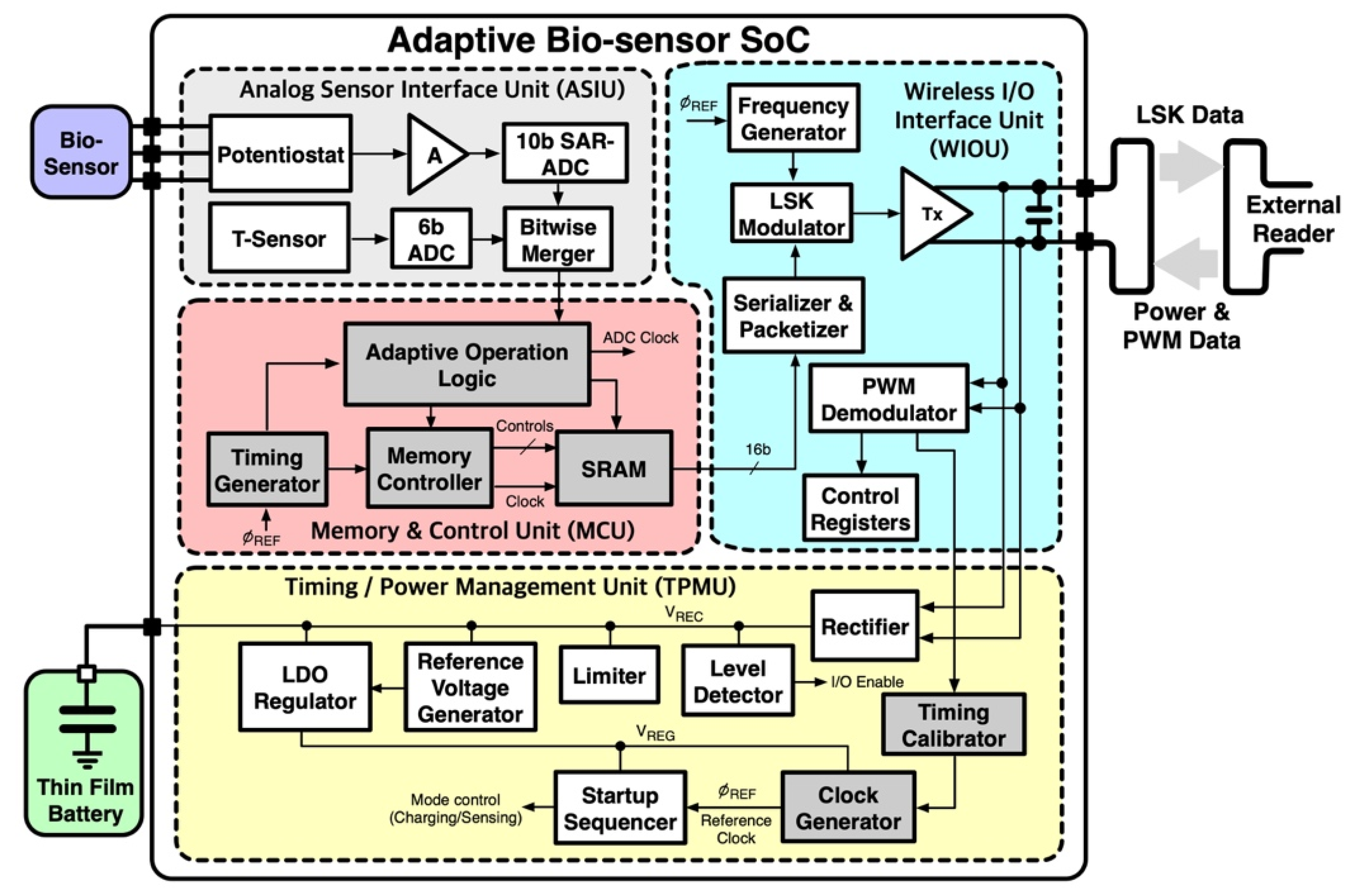
2. Biosensor SoC Architecture and Circuits
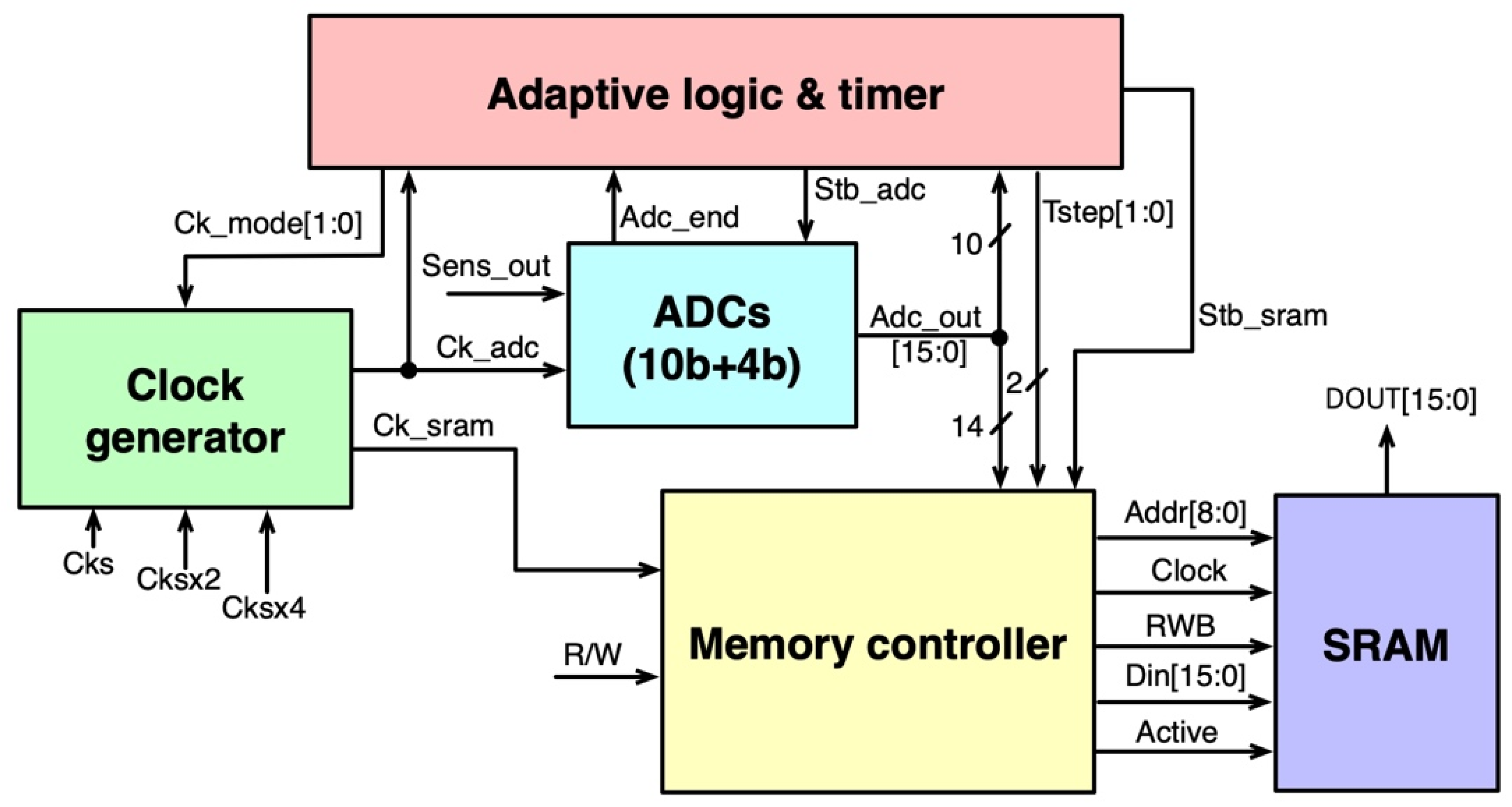
The proposed implantable biosensor SoC (
Figure 2) consists of an analog sensor interface (ASI), which includes two SAR-ADCs for bio-signals and body temperature sensing, a wireless I/O interface (WIOI) to engage in magnetic coupling with external reader for data and power telemetry, a memory and control unit (MCU) for adaptive data recording in the SRAM, and timing/power management unit (TPMU) for the reference clock and supply voltage generation. When the biosensor SoC is inductively coupled with an external reader, the charging of an internal battery through a rectifier, registration of initial control parameters modulated using pulse-width modulation (PWM), and the calibration of internal oscillator are initiated in turn via the predefined startup sequence in the power management unit. Then, the recorded datasets from the SRAM are serialized, modulated by load-shift keying (LSK) [
12,
18], and wirelessly delivered to the external reader. During this period, the analog sensor interface unit stops sensing and collecting bio-signal data while the rectified power is charging up the internal battery.
When data transmission ends and the coupling with external reader is removed, the analog sensors resume sensing operations and start to use battery power, convert the input analog signal to 16-bit binary data (10-bit for bio-signal, 4-bit for body temperature, 2-bit for mode indexing), and store data in the internal memory. In the next three sub-sections of this paper, we describe the proposed key circuit techniques for the implementation of biosensor microsystem for long-term monitoring purposes.
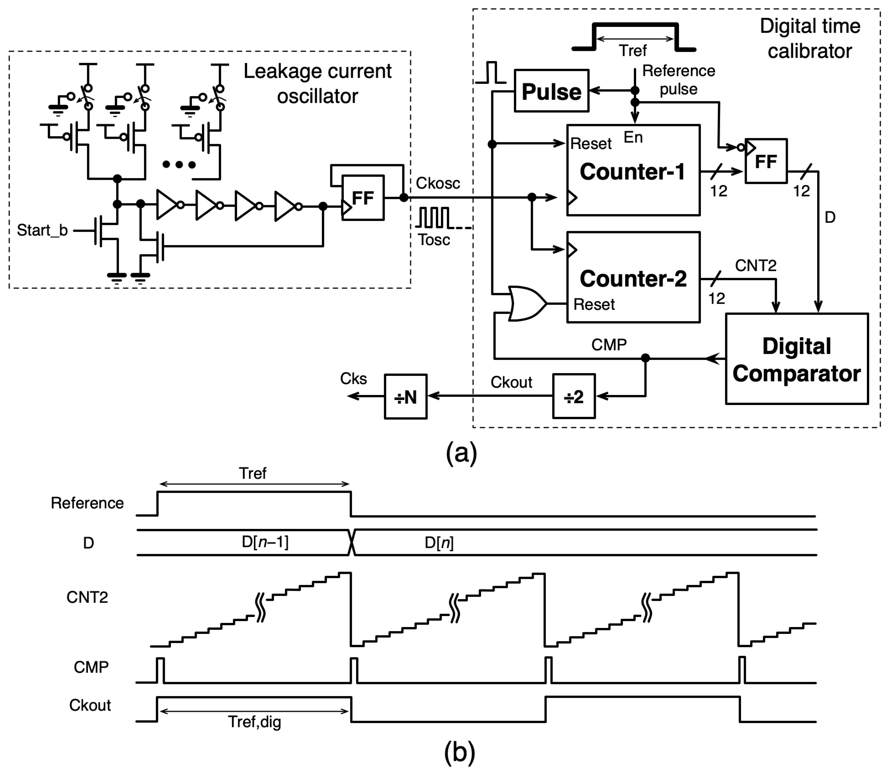
2.1. Clock Calibration Scheme
During all operation periods of the proposed biosensor SoC, most circuits in the TPMU blocks remain in the ‘ON’ state and consume constant power, since the regulated supply voltage and the reference clock should be provided without interruption. In particular, the clock generator should continuously run to supply power to the clock in the analog sensor interface unit and memory circuits. A leakage-current-based oscillator [
19,
20,
21] can be a good candidate for this purpose, since it provides large time constant for extremely low duty-cycled operations and consumes only picowatts. However, the challenging issue of using this circuit is its high sensitivity to PVT variations. To overcome this problem, a periodic calibration scheme is necessary to prevent the frequency error of the circuit from accumulating over time. A reference clock for the calibration can be internally generated using an RC-based relaxation oscillator [
12]. However, embedding an RC-based relaxation oscillator may cause significant power dissipation and is not a feasible option. Instead, the calibration procedure can only proceed in the event of external charging when a reference pulse (T
ref) is provided by an external reader, as shown in
Figure 3a. This scheme seems to be feasible since the frequency changes in the leakage-based oscillator due to the temperature variations are well linked to the thermo-regulation mechanism of the human body. A digitally assisted initial tuning scheme can also be implemented against process variations.
The proposed internal clock generation scheme consists of a leakage-current oscillator and digital calibration scheme (
Figure 3a). A digitally assisted control adjusts the amount of leakage current by approximately 3.5 times. At the rising edge of reference pulse (T
ref), both counter-1 and counter-2 are enabled and start counting the number of rising edges of clock from the oscillator (Ckosc). When the reference pulse becomes low, counter-1 stops counting and stores its 12-bit binary output in registers. A digital comparator compares the two binary outputs from the registers (D) and counter-2 (CNT2) and generates an output pulse (CMP) whenever they match, resetting both counters as shown in
Figure 3b. The following frequency dividers convert this output pulse to the internal clock (Cks).
In this way, provided that the period of the reference timing pulse (Tref) is well within the maximum time length of binary counters, the reference pulse (Tref) can be converted to digitized time data (i.e., Tref,dig = D[n] × Tosc), and the period of the output clock is fixed to 2 × Tref,dig during the sensing operation. Finally, any deviations of clock period owing to environmental variations from the digitized reference can be calibrated whenever the reference pulse is provided from external readers.
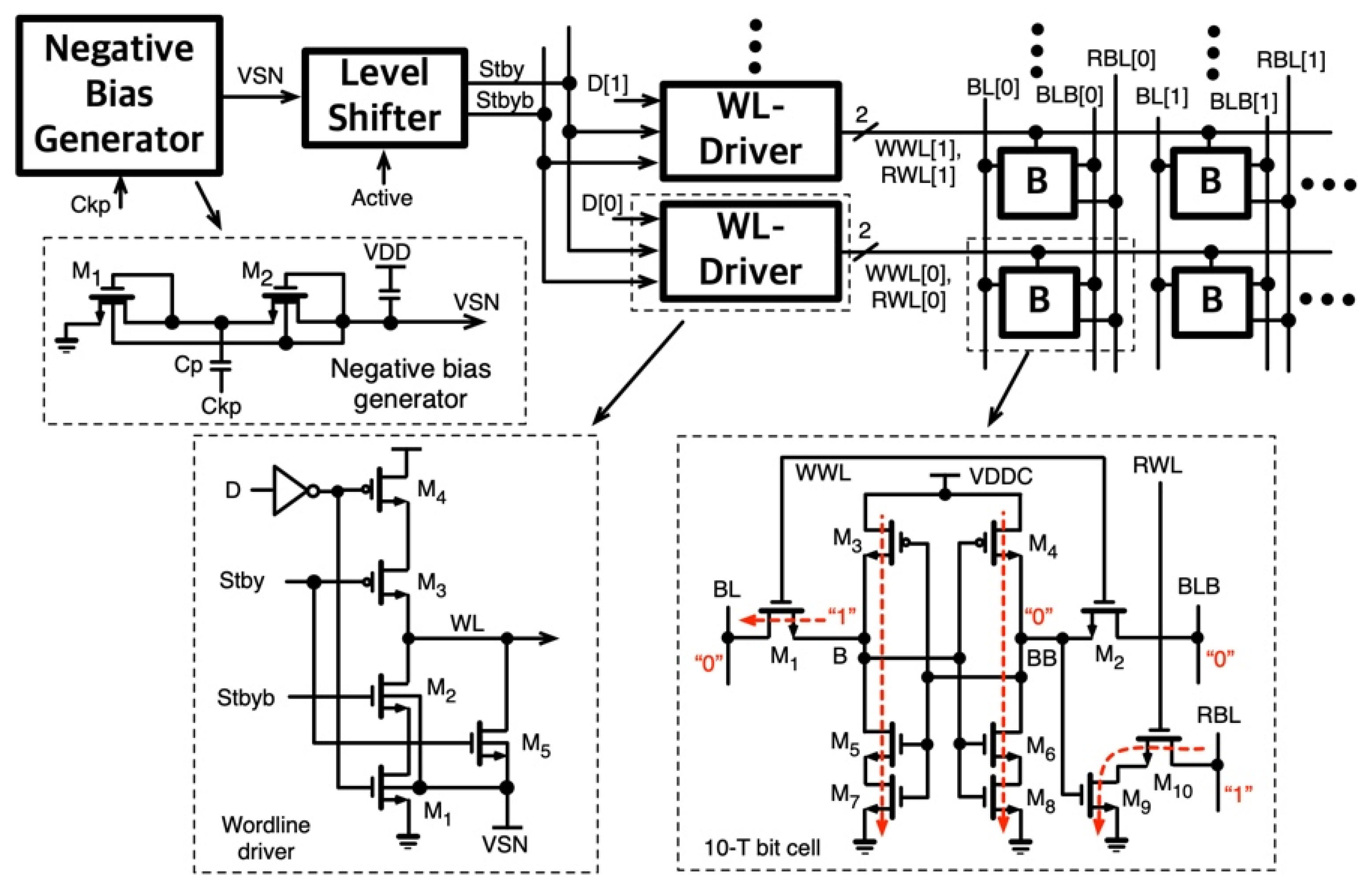
2.2. Ultra-Low-Standby-Power SRAM
The ultimate design principal of the SRAM embedded in the implantable biosensor SoC is to lower the power consumption and extend usage time until the next charge. Under extremely low duty-cycled (<<0.1%) conditions, power consumption in standby mode as well as active mode becomes very important. This is because small leakage current in a storage cell can greatly contribute to total standby power consumption in large cell array. In the proposed 8K-bit SRAM, we utilized an 8-T-based cell [
22] to maintain the reliable noise margin at low supply voltage (0.4 V) and have a negative wordline scheme [
23,
24,
25] to further minimize leakage current.
In conventional 6-T cell, lowering the supply voltage can be constrained by write margin and read stability issues [
22]. To solve this problem, the read port can be decoupled from a basic 6-T cell by adding additional two transistors (M
9, M
10 in
Figure 4) with a separate wordline (RWL) and bitline (RBL) for read mode. In this way, the read operation itself no longer compromises cell stability at a lower supply voltage. This is because the read operation that enables RWL and RBL for a target cell no longer has any possibility of affecting the contents of memory latch (M
3~M
6). Because of this robustness, stability (or degree of data retention) at a lower supply voltage can be significantly improved.
In standby mode, total cell current consists of leakage current through the latch transistors (M3~M8) and pass gates (M1~M2, M10). In the proposed 10-T cell, P-N-N-type latches were adopted by adding NMOS (M7, M8) at the bottom to reduce vertical direction leakage current. The leakage current through the pass gates (M1~M2, M10) depends on the stored data value and precharge states of bitlines. To remove this dependency and minimize leakage current, the memory cell uses negative voltage (VSN) across both wordlines to keep the pass gates in super cutoff state in standby mode.
In the proposed SRAM, each wordline driver has gating (M
2, M
3) and pull-down transistors (M
5) to driver negative voltage (VSN), as shown in
Figure 4. When standby mode is enabled (Stby = H), the driver output turns into a high-Z state and the pull-down transistor (M
5) turns into the “ON” state pulling down wordline voltages to VSN. To prevent leakage current through the substrate, NMOS transistor bodies are tied to lowest voltage (VSN). Additionally, the opposite control signal (Stbyb = L) must be a negative voltage so that the pull down path through M
2 and M
1 transistors is blocked.
For the generation of negative supply voltage (VSN), a charge pumping scheme [
26,
27] was adopted, as shown in
Figure 4. A single-stage pumping conforms with our requirements by removing the use of un-overlapped differential clock phases. Within the −0.1~−0.2 V range, the output voltage level can be adjusted by controlling the size of AC-coupled capacitance (Cp).
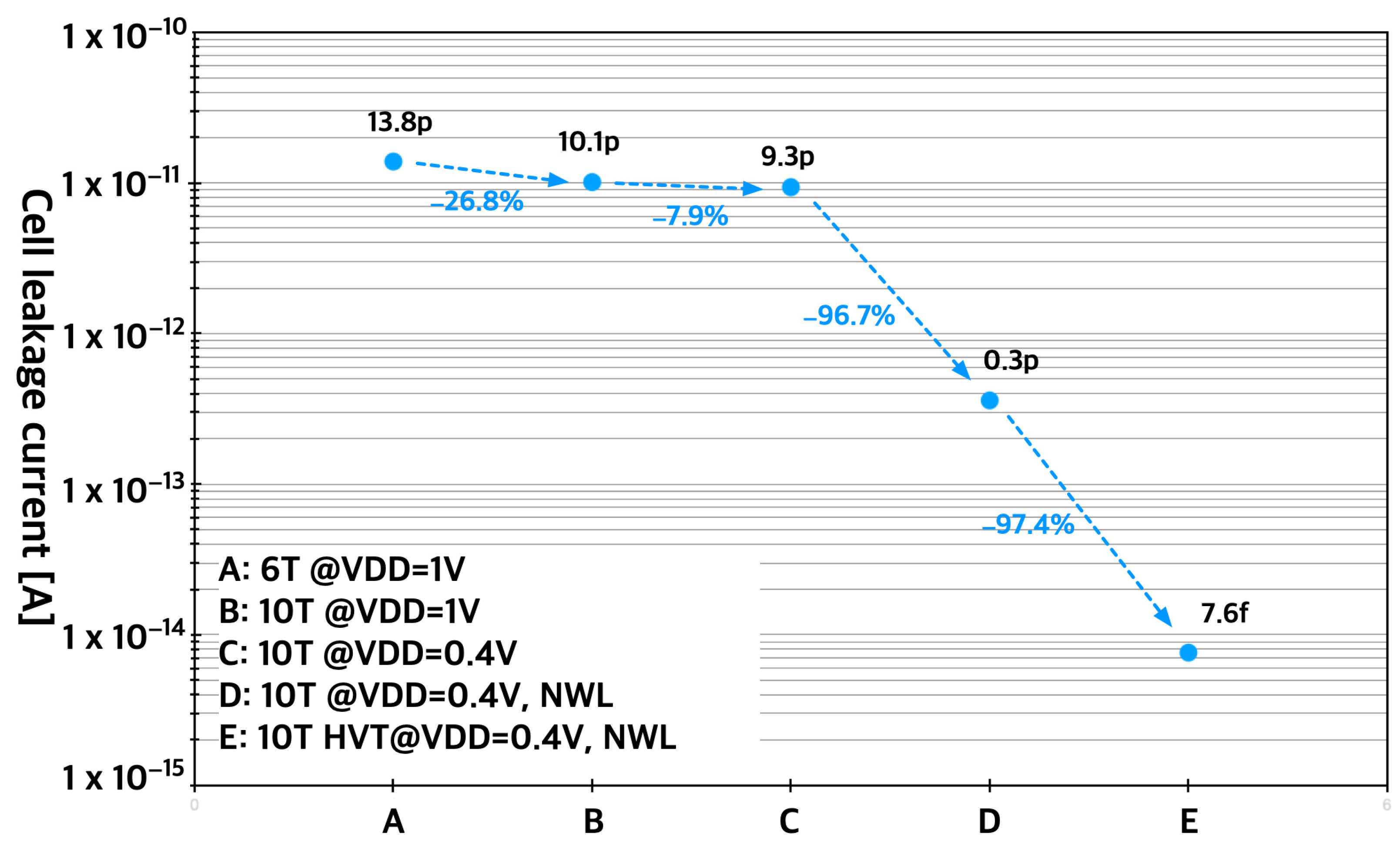
Cell leakage current has been evaluated to estimate the effect of cell topologies, supply voltages, wordline driving voltages, and transistor types, as shown in
Figure 5. Compared to a conventional 6T-based cell at a nominal supply voltage (1 V), the leakage current of the proposed 10T cell can be reduced by 26.8% and 7.9% at 1 V and 0.4 V supply voltages, respectively. When the negative wordline technique and high-threshold device (3 V I/O transistors) are adopted, the leakage current is dramatically reduced, achieving about −96.7% and −97.4%, respectively in the proposed 10T cell. By applying these techniques, the overall leakage current can be reduced by 1815 times when compared to conventional 6T cell. Although the effect of cell topologies may not seem very attractive, the 10T cell provides a sufficient voltage margin and cell stability at low supply voltages.
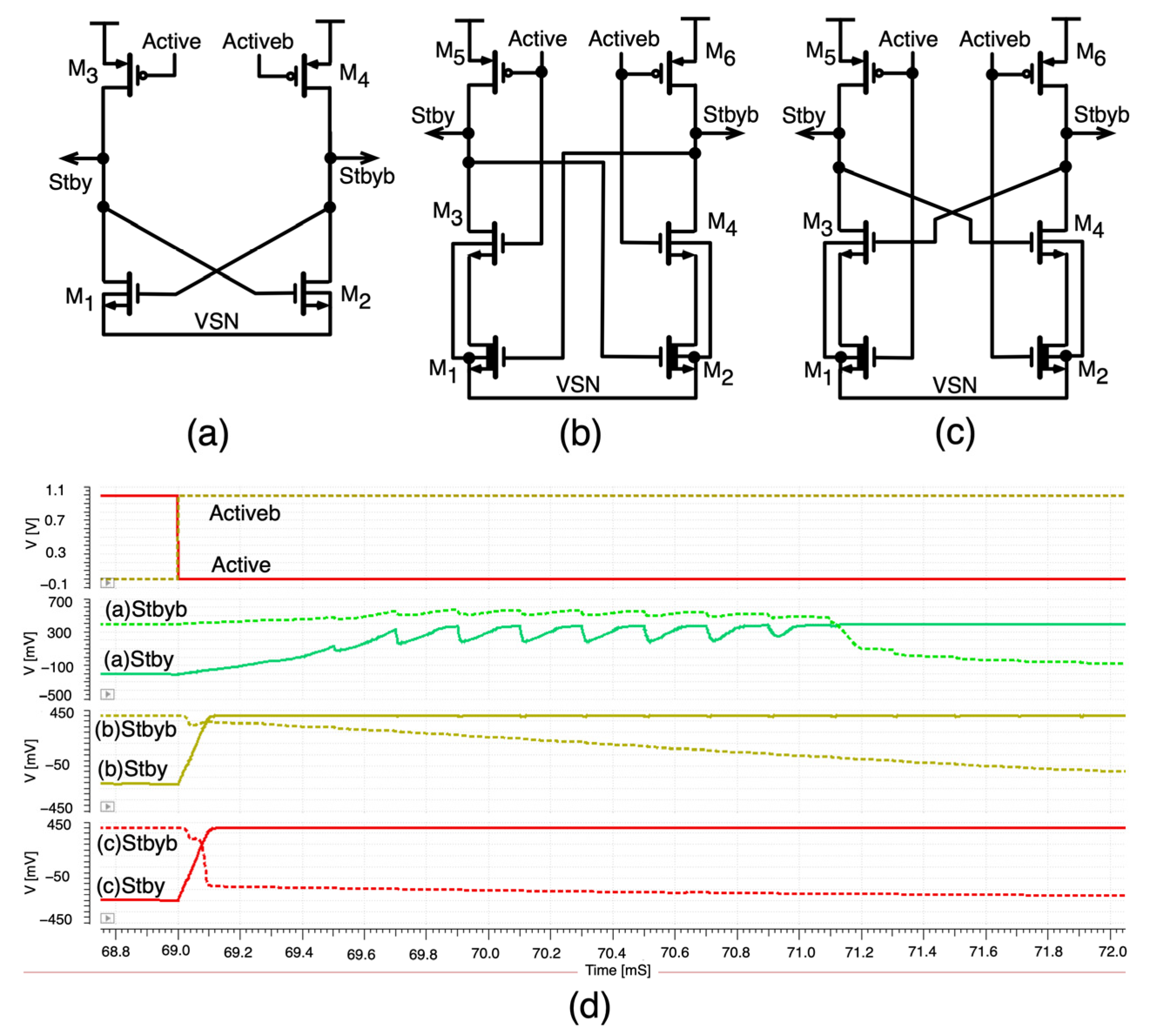
The command signals (Stby, Stbyb) in the wordline drivers need to swing from supply voltage to a negative voltage, so a level shifter circuit is necessary between the bias generator and driver. However, conventional level shifters [
28,
29], as shown in
Figure 6a,b, often have a time delay between their differential output signals, which results in a significant amount of short-circuit current at the wordline driver circuits. This happens because the negative bias generator has a finite output resistance, and the level shifter circuit has to drive a heavy load. To alleviate this problem, we propose a new level shifter, as shown in
Figure 6c, in which pull-down NMOS directly responds to the command signals, isolating output signals from the earlier VSN node. In addition, high-threshold transistors are used for the bottom NMOS (M
1, M
2 in
Figure 6c) to further reduce vertical current flowing through the latches.
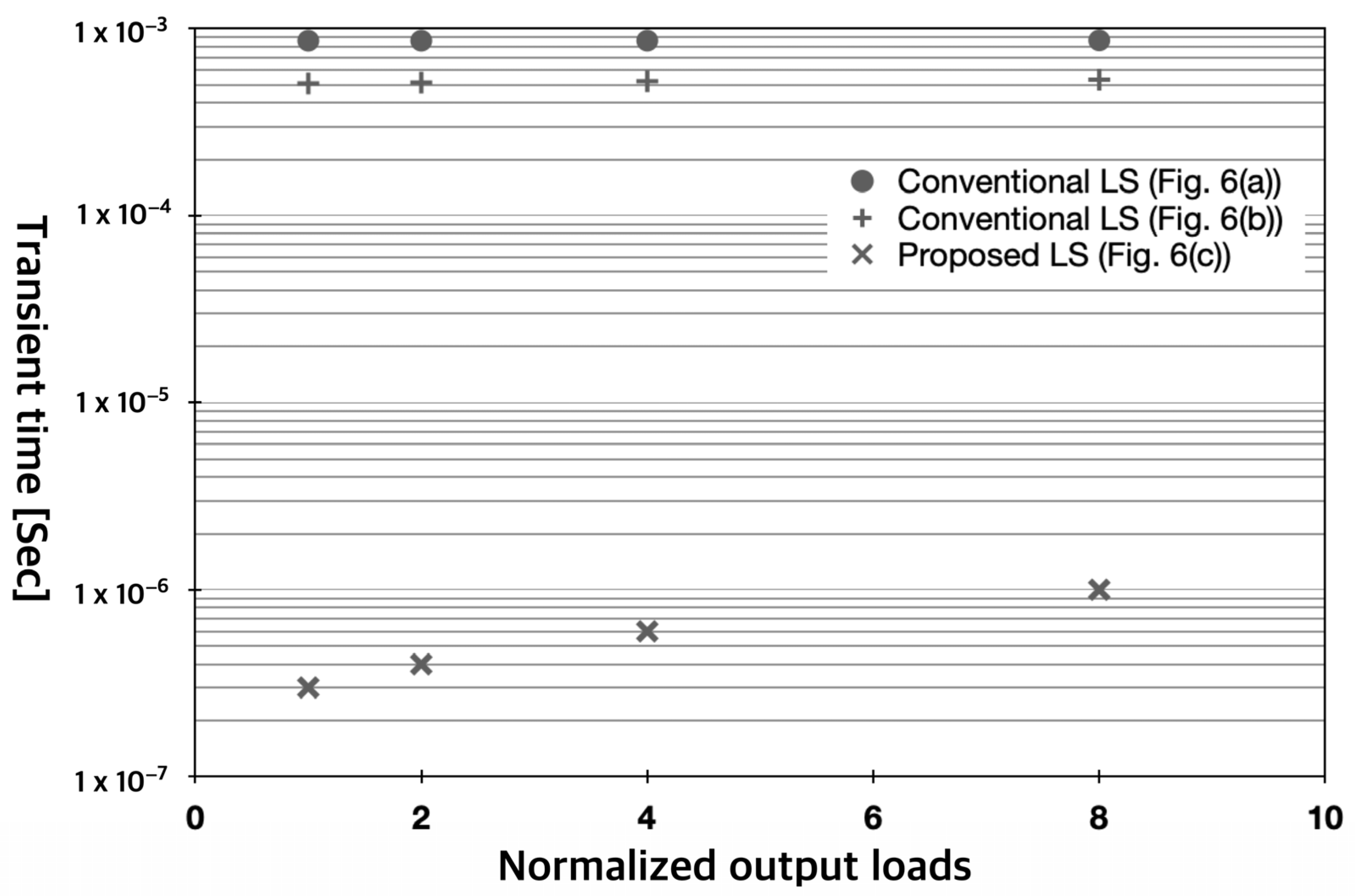
The proposed level shifter exhibits a much faster output transition when compared to conventional ones in the simulation as shown in
Figure 6d. The average current dissipation of level shifters in
Figure 6 are 32.8 pA, 13.8 pA, and 9.5 pA, respectively. Thus, the proposed level shifter not only has a faster output transition but saves significant power dissipation (71~31%). The output transition time was evaluated as a function of normalized output load in the presence of negative voltage (VSN), as shown in
Figure 7. The proposed level shifter demonstrates its superiority by implementing a very fast transition compared to existing level shifters. As the output load increases, the transition time change in the proposed level shifter becomes somewhat steeper than that in conventional level shifters, demonstrating the superior dynamic behavior of the proposed shifter under conditions of negative supply voltage.
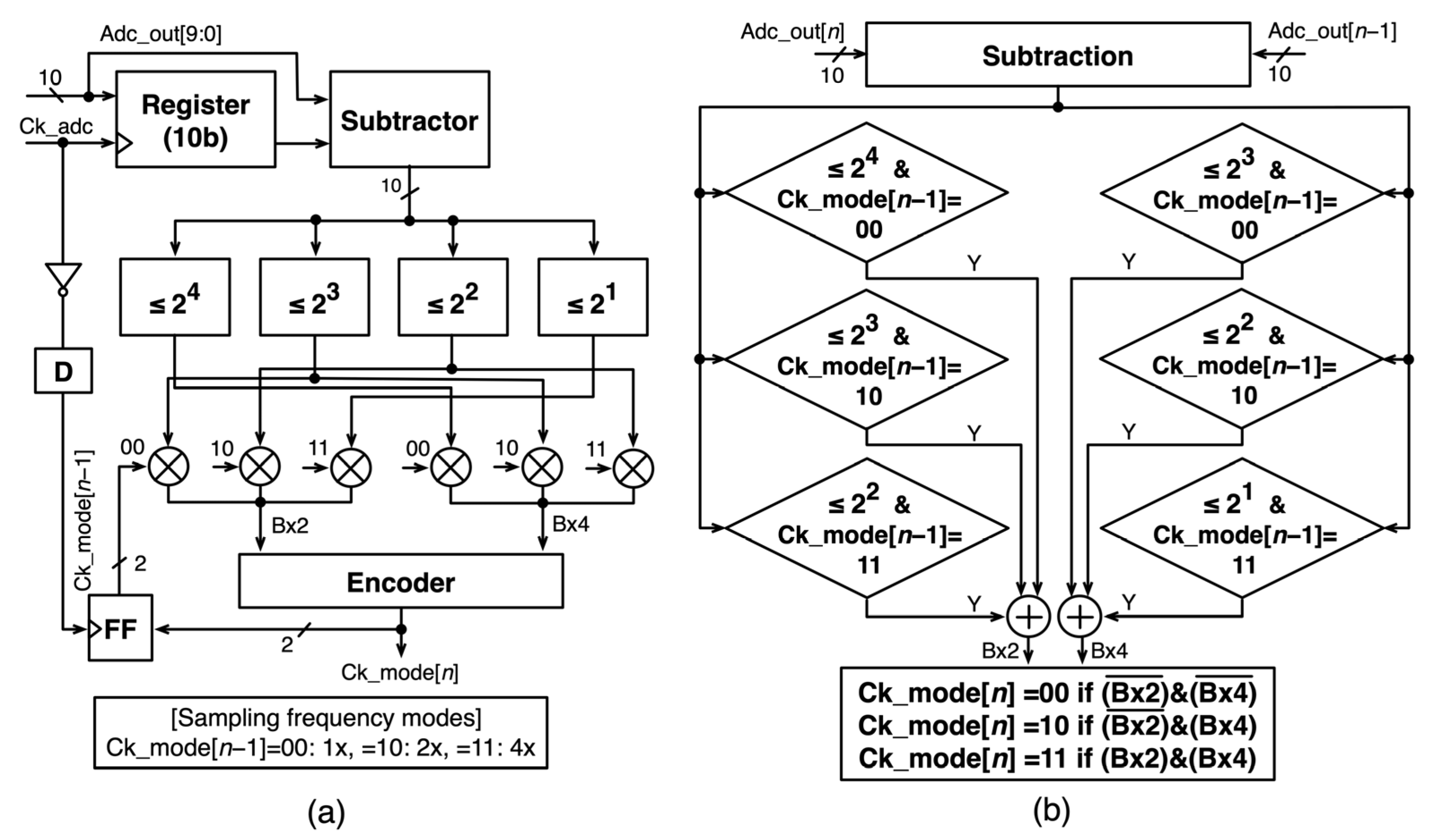
2.3. Adaptive Sensing Scheme
At a given time of usage, the sampling frequency (or sensing time period) actually determines the size of storage, which is often constrained by a tight area and power budget. To efficiently collect daily excursions of bio-signals and perform an individualized diagnosis of the disease, it is highly necessary to implement an adaptive sensing scheme with an adjustable sampling frequency that proportionally changes with the bio-signal. In this way, the usage of data storage can be efficiently managed without losing important information.
The proposed adaptive sensing scheme is shown in
Figure 8. The clock generator accepts three different clock frequencies, which are one (Cks), two (Cksx2) and four (Cksx4) times the nominal sampling frequency. These frequencies generate an operation clock for ADC and SRAM based on the clock mode signal (Ck_mode[1:0]) which represents the rate of bio-signal changes. In adaptive logic and timer (ALT) units, the current ADC output of the analog sensor (10b) is compared with its previous output, and the resulting magnitude of their difference determines the clock mode. To identify from which sampling frequency an ADC output is generated, two tag bits (Tstep[1:0]) are assigned to label the clock modes. These tag bits are used to identify the exact timing of data sensing at the time of data retrieval by the external reader.
The memory controller (MC) receives 16 bits of data from an analog sensor (10b), temperature sensor (4b), and clock mode tag (2b) as data inputs for the SRAM, and then generates control signals for the 8K-bit-size memory. In the read mode, the MC unit simply operates as an incremental counter to support sequential read operations.
The block diagram of adaptive sensing scheme is depicted in
Figure 9a. To compare the previous digitized 10-bit sensor output (Adc_out[9:0]) to the current output, 10-bit registers and a subtractor are used to generation 10-bit difference outputs. The following four digital comparators compare their magnitudes to 2
4, 2
3, 2
2, and 2
1, respectively. However, the magnitudes of difference outputs are relative magnitude depending on the current sampling frequency which is defined by 2-bit Ck_mode[
n−1] data. For example, if the current sampling frequency is 2×, then the difference is only half the amount that can be obtained using a 1× sampling frequency. Therefore, the current sampling frequency must be taken into account when evaluating magnitude changes in the sensor output.
To this end, pass gate logic is implemented to flag the Bx2 signal if the subtractor output is larger than 2
3 for 1× frequency, 2
2 for 2× frequency, and 2
1 for 4× frequency, respectively. If any of these cases is satisfied, the Bx2 signal is set. Likewise, the Bx4 signal is set if the subtractor output is two times larger than that of Bx2 signal. The state diagram in
Figure 9b shows the algorithm. According to Bx2 and Bx4 signals, the next clock frequency (Ck_mode[
n]) will be determined. In this way, the sampling frequency and clock frequency for SRAM adaptively changes according to the rate of change in the digitized analog sensor output.
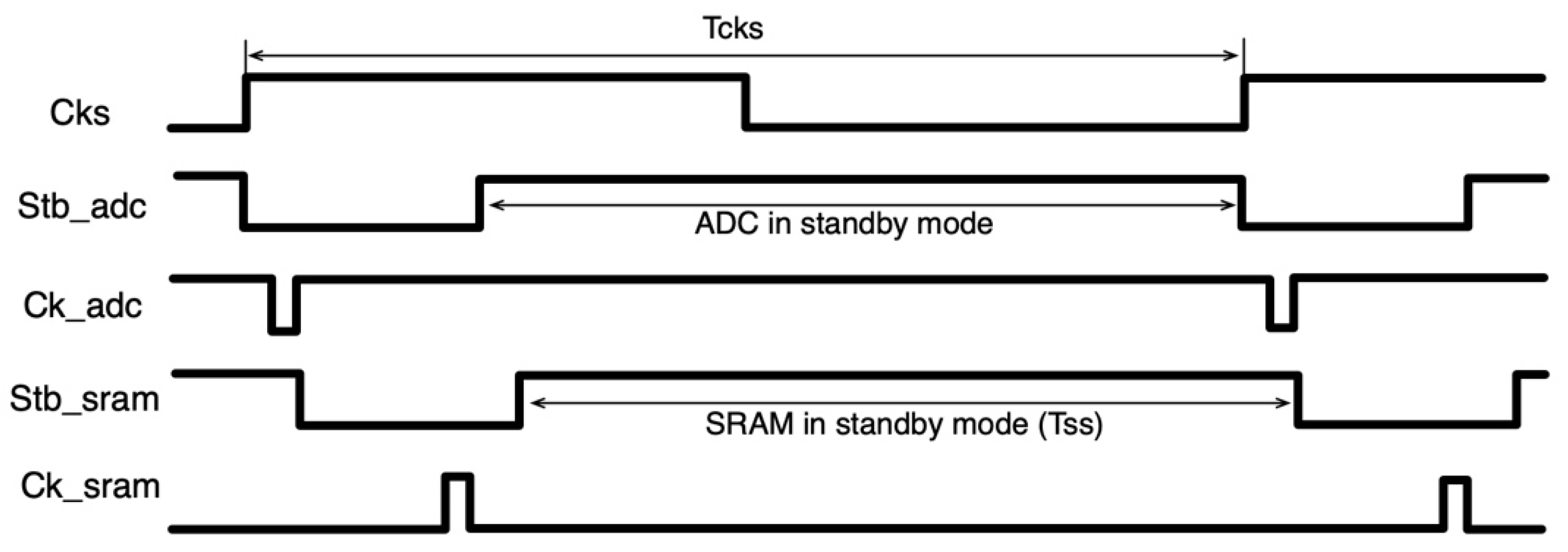
Another pivotal role of ALT unit is to set the timing of standby signals (Stb_adc and Stb_sram) for ADC and SRAM, as shown in
Figure 10. Within one cycle of the reference clock (Cks, Cksx2, or Cksx4), the ADC and SRAM are activated just once to sample bio-signal and store digitized data in one memory address. Once this operation is finished then each ADC and SRAM stays at standby mode until the next clock cycle.
3. Experimental Results
The key operation schemes of proposed biosensor SoC (
Figure 2) has been implemented in commercial CMOS 180 nm technology for the circuit simulation. Transistor-level fully customized designs such as a leakage-based oscillator, its digital calibration scheme, 8Kbit SRAM circuits and adaptive sensing scheme, and corresponding circuits for comparative studies (oscillator calibration method, standard 6T-based 8Kbit SRAM, conventional level shifters, and single-period sensing scheme) were implemented in schematic editor (Cadence Virtuoso
® v. 6.1.7-64b). Circuit-level simulations (Cadence Spectre
® v. 15.1.0.644.isr13) were performed to characterize performance based on the netlist extracted from the schematic editor.
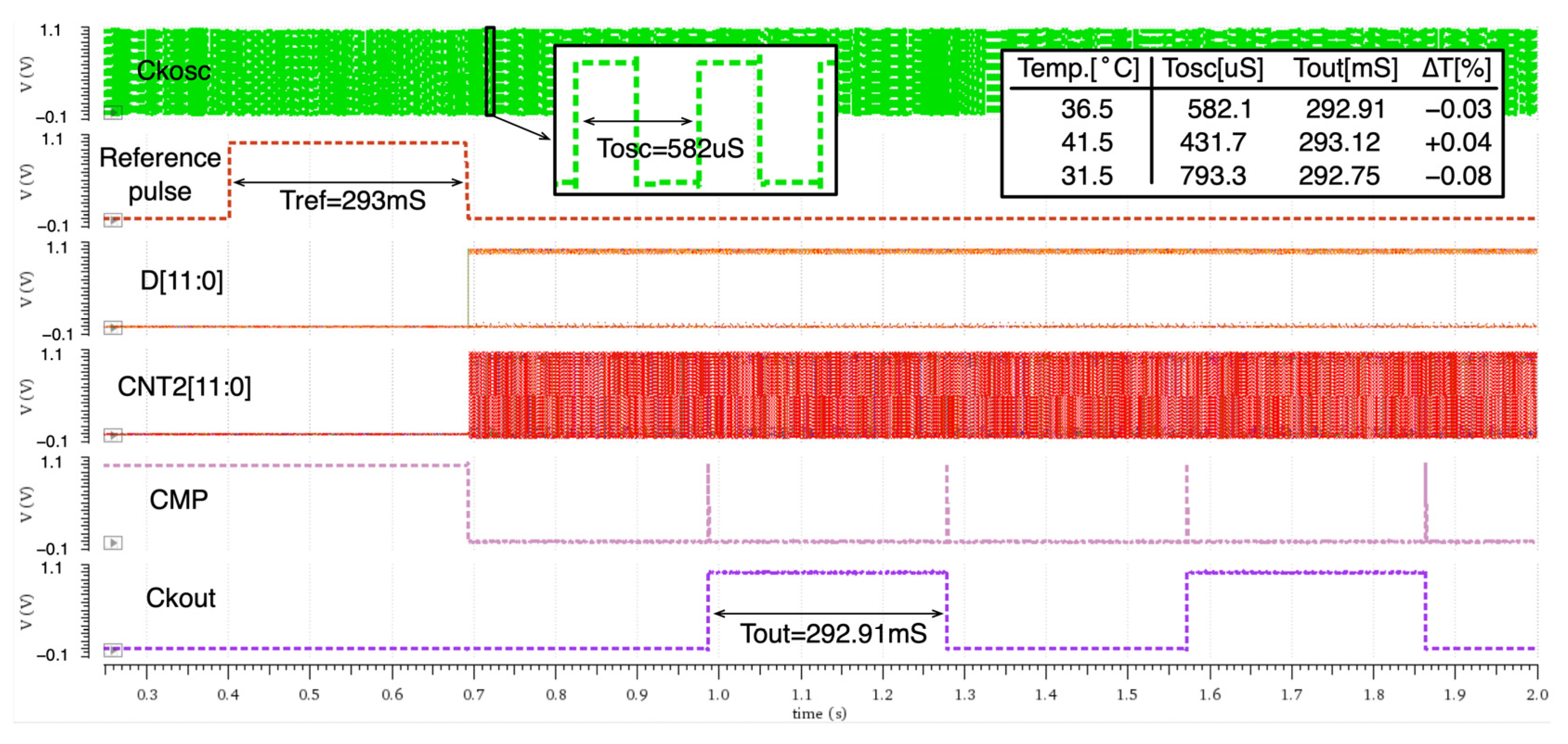
If we assume that a bio-signal is gathered every 5 min (300 s), the reference pulse width (Tref in
Figure 3) for the internal timing calibration is about 293 mS (=300/1024). The time period for the leakage-current oscillator was 582 uS at 36.5 °C, and the simulated signal waveforms of reference clock calibration scheme are presented in
Figure 11. The time period for the leakage-current oscillator can be adjusted with 2-bit digital switches (
Figure 3) and its adjustable range covered from 295 uS to 1.15 mS. The performance of timing calibration has been tested at three different extreme body temperatures: 31.5 °C, 36.5 °C, and 41.5 °C. The periodic error for the calibrated clock output (Ckout) was well within 0.1% of the reference pulse (Tref) at these temperature corners, as summarized in the table shown in
Figure 11.
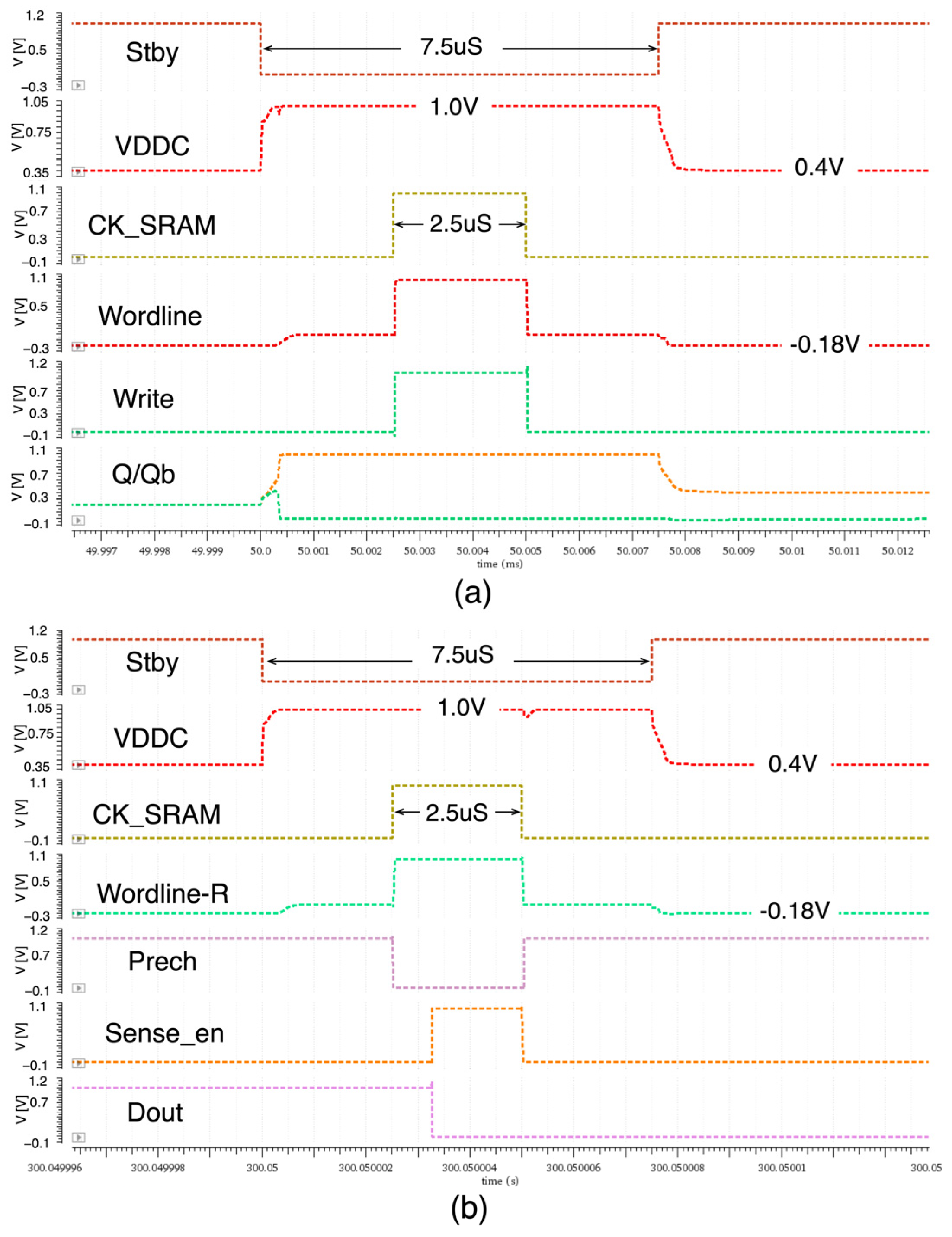
The 8K-bit SRAM with 16-bit IOs was designed to verify its operation under the proposed dynamic voltage scheme. When the write (
Figure 12a) or read (
Figure 12b) operation was initiated by the falling of standby signal, the supply voltage of the cell array (VDDC) and wordline voltages increased from 0.4 V and −0.18 V (standby mode) to 1 V and 0 V (active mode), respectively, before the clock arrived. The actual write/read operations could be completed within 2.5 uS of clock pulse. Following the increase in standby signal (Stby), the SRAM enters into standby mode again. During the active mode (7.5 uS), the average power consumption of the proposed SRAM was about 97.8 uW.
Figure 13 summarizes percentile average power consumption of SRAM blocks in standby mode. In conventional SRAM, most of power dissipation was caused by large number of bit cells and wordline drivers (64 for write and 64 for read). However, in the proposed SRAM, their contribution to the total power dissipation significantly decreased with the help of supply voltage scaling and a negative biasing scheme. Including 27 pW of negative bias generator, the control/biasing block occupies most of power consumption (33%). Total 8 K-bit cells dissipate at about 23.85 pW and each bit cell only consumes 2.9 fW. In summary, the proposed SRAM that adopts negative wordline and supply voltage scaling saves about 70% of power consumption compared to conventional SRAM. The overall average power consumption including active and standby mode was about 112 pW.
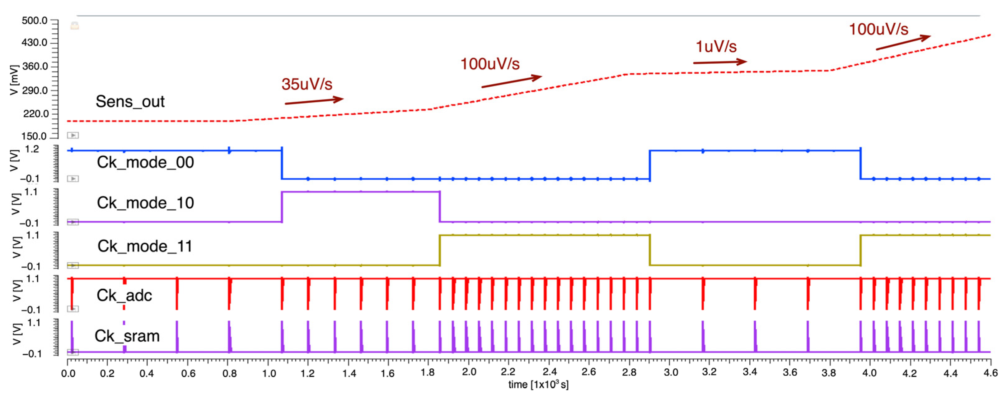
The proposed adaptive sensing scheme (
Figure 8) can be implemented in circuit simulation, and its operation waveforms are shown in
Figure 14. When the ADC input (Sens_out) changes at various rates, the ALT block senses its variation rate from digitized data (Adc_out[9:0]) and determines the next sampling clock frequency (Ck_mode) based on the current mode. The sensing clock period (Ck_adc) is adaptively chosen from 5, 2.5, or 1.25 min as the rate of bio-signal changes from 1 to 100 uV/s range. Therefore, the digitized 16-bit data from the bio-signal sensor, temperature sensor, and corresponding mode detector are stored in SRAM, which is synchronized to the adaptively updated clock period (Ck_sram). Compared to the case where the same sensor inputs are sampled every 1.25 min, which is the shortest sensing period, the proposed adaptive approach saves about 42.8% of storage space. The implication of this result is that variations in biomarkers during daily activities in the patient’s body can be collected 57.2% more rapidly, without sacrificing detailed information. Additionally, by extending the concept of this approach, more sophisticated bio-signals than usual can be possibly captured by sacrificing storage space or usage time.
In
Table 1, the power consumptions of circuit blocks were compared to previous research, in which the bio-signal (glucose level in teardrops [
12]) could be detected only when the external reader was present. Except commonly shared circuit blocks, the newly added circuit blocks do not consume significant power, except for the temperature sensors, and the total power consumption was even reduced by 42% compared to previous research. The major contributions of low-power dissipation were achieved by removing RC-based internal oscillator, which was necessary to provide a reference clock for the calibration of a leakage-based oscillator in the previous implementation and utilizing extremely low-power techniques for the SRAM design and its control circuits. When a thin-film battery with a 5 uAh capacity (CYMBET
® (Elk River, MN, USA) 1.7 × 2.2 mm
2 [
30]) is used, the proposed biosensor SoC is expected to perform a sensing operation for about 60 h (2 and a half days) without externally supplied power.
The functionalities of the proposed biosensor system are compared to the existing functionalities, as shown in
Table 2. Because the implant of a proposed system contains a battery and storage system, the energy of the battery is used for the bio-signal detection and data accumulation. However, previous research often caused inconvenience to patients by performing either a one-time reading [
12] or read-while-contact [
10] functionality, while consuming energy momentarily transferred from external readers and accumulating data in external reader. The novelty of the proposed system lies in the fact that it uses key circuit techniques to alleviate the issues with existing approaches. The major drawback of the proposed system may be its limited storage capacity compared to existing systems. However, it has been proved that the proposed low-power circuit techniques and adaptive sensing scheme can alleviate these limitations to some extent.


