1. Introduction
In order to implement Industry 4.0 to achieve applications such as smart factories, machine control, and data acquisition, it is necessary to use technologies such as the Internet of things and sensors. Among them, the Internet of things connects computers and other industrial equipment through the network, which will make the network structure more and more large, and the transmission of data depends more on real-time. Common network time synchronization methods include GNSS, NTP, and PTP, etc. The GNSS clock signal is transmitted through radio waves and special equipment must be installed on the application device, so the cost is relatively high. However, NTP has the lowest cost. In the industrial Internet of things (IIoT), the network time protocol (NTP) can be used for time synchronization [
1,
2]. NTP is low-cost and easy to use, but it can only provide millisecond-level time precision, which cannot meet the precision required by modern measuring instruments and industrial control. Therefore, the IEEE Society proposed the Precision Time Synchronization Protocol (PTP) in 2002, also known as IEEE 1588. The second edition of IEEE 1588–2008 [
3] was revised in 2008, and the latest version is the third edition of IEEE 1588–2019 [
4], released in 2019. PTP is a synchronization protocol for periodic packet exchange using Ethernet, using primary/secondary architecture; its advantage is that it can be achieved by using the existing Ethernet line, which makes the deployment of the time synchronization network easier.
Regarding the research on IEEE 1588, B. Zhao [
5] implemented a design scheme of FPGA, DM9000, and DP83640 based on the detailed analysis of IEEE 1588 protocol and the best primary clock algorithm (BMCA), through the integration of software and hardware. Verified by experiment, the system can realize sub-microsecond level time precision in synchronization with the primary clock and secondary clock. Their design improved the time synchronization precision and simplified the hardware circuit design. N. Moreira [
6] discussed the implementation of the PTP function on the Xilinx Zynq-7000 SOC development board. The experimental environment is to use one development board as PTP primary and the other development board as PTP secondary and use an oscilloscope and a computer to view the PPS (pulse-per-second) signals generated by the device and the message of the PTP console at the same time. PPS is a signal that outputs a high logic level once a second and the pulse width is generally 100 ms. It can be applied to smart grids and substation automation systems and can meet reliability requirements. S. S. W. Lee [
7] proposed two architectures to realize the OpenFlow switch with the PTP function. The first architecture is to embed the designed PTP module in a NetFPGA-based OpenFlow switch. The second architecture is to use the designed PTP module as an add-on module to work with a PTP unaware switch. The results show that the PTP module can implement a software-defined time synchronization network, and can meet the precision standards of microsecond-level small wireless base stations. Z. Idrees [
8] compared common time synchronization technologies, such as GPS, NTP, and PTP, and concluded that PTP is the most stable clock synchronization technology, and also proposed many methods to improve the accuracy of PTP, including boundary clock optimizations, modifications in IEEE 1588 messaging, improved internal clock stability, etc. Due to the rapid development of artificial intelligence algorithms and the establishment of smart factories, especially distributed optimization (DO) on multi-agent networks, has been extensively studied [
9]. Time synchronization is an important key. All devices on the network need to have a common time reference so that all devices work together and take fast actions at precise times.
In this paper, firstly, we implemented the Linux PTP hardware solution on the Xilinx Zynq-7000 SOC platform of Petalinux. The hardware timestamp is 20 ns. To improve accuracy, we propose an IEEE 1588 (PTP) chip design and implementation with dynamic frequency compensation. Experimental results show that the 45 nm (TN40G) node can work at 370 MHz with a resolution of 2.7 ns. The final calculated time offset is 10.8 ns. The core of the IC we designed can be integrated into related communication chips, it can be applied to a related communication network card, and this communication network card has the function of fast time synchronization.
The rest of this article is structured as follows. In
Section 2, we will introduce PTP. In
Section 3, we illustrate the implementation of system timestamps, including software timestamps and hardware timestamps. In
Section 4, we illustrate the IC design and implementation of PTP hardware-assisted time stamping. Experimental results and analysis will be placed in
Section 5.
Section 6 provides conclusions.
2. Precision Time Protocol Introduction
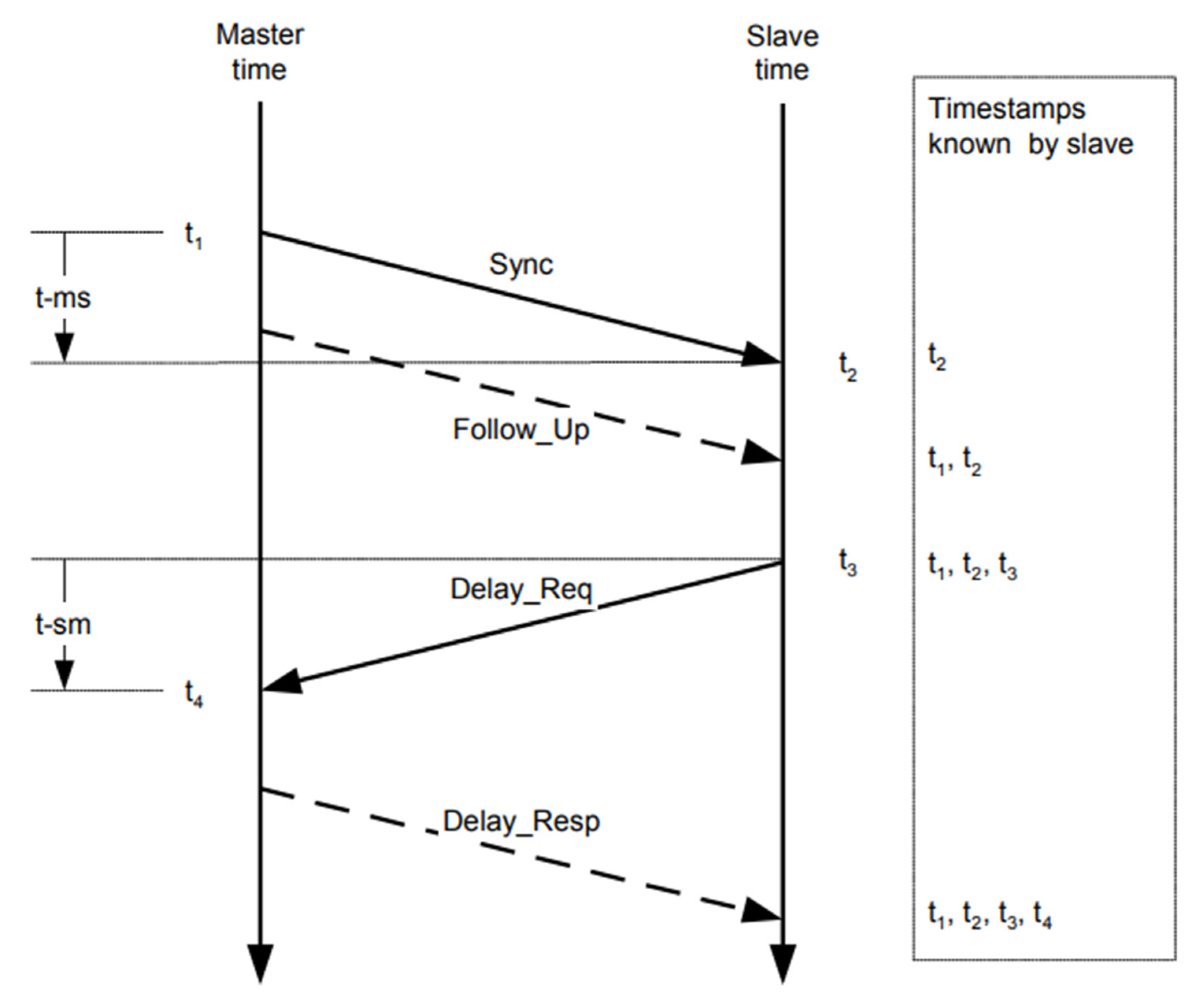
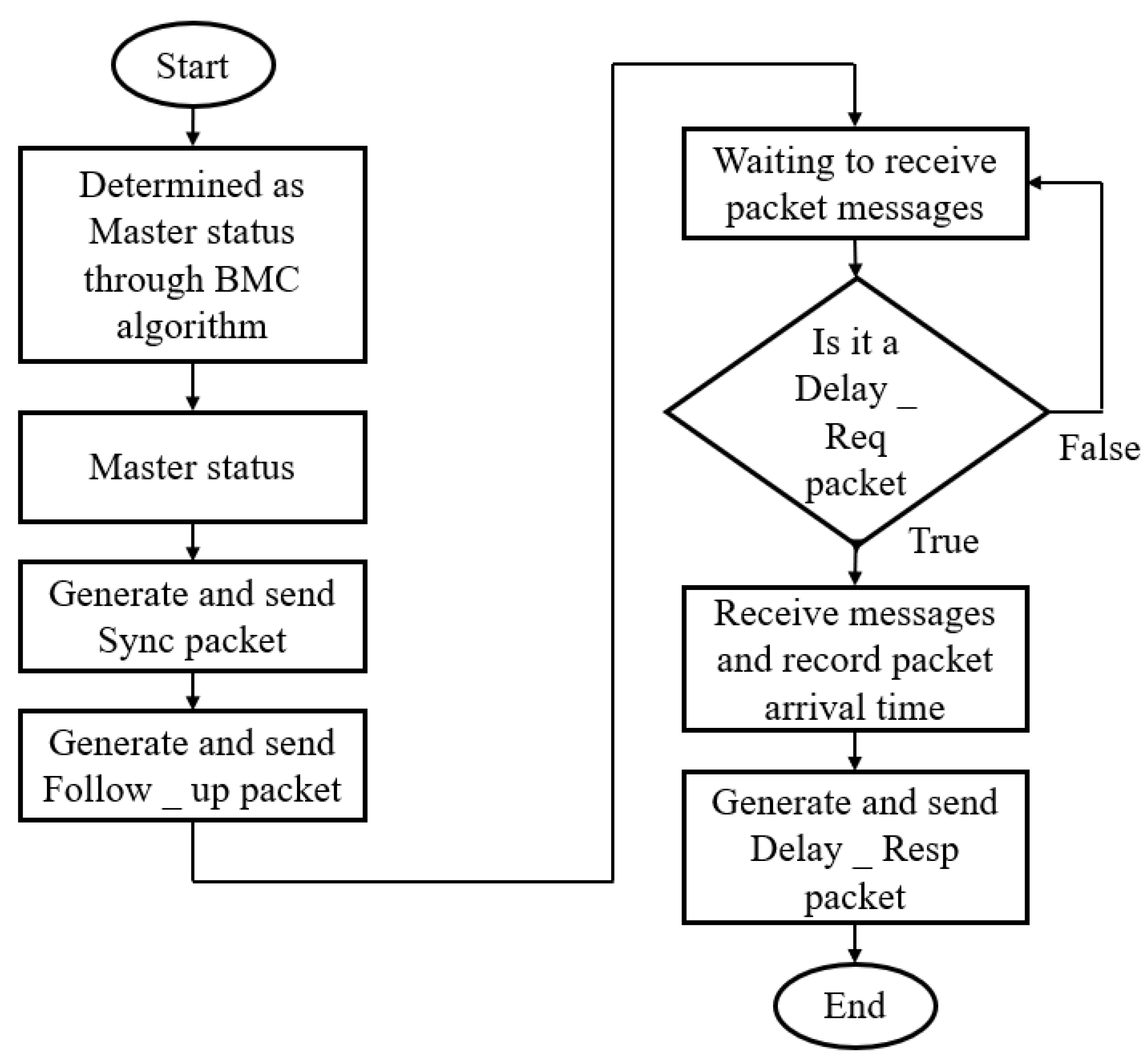
The PTP protocol sends periodic packets to each node in the network through the Ethernet to confirm the system structure of the entire network and transmit time information to achieve synchronization between different clocks. PTP defines a relay request–response mechanism to measure the offset of Primary and Secondary. It calculates the sending and receiving time by sending Sync, Delay_Req, Delay_Resp, and Follow_up packets, as shown in
Figure 1. Using the timestamp generated by the above-mentioned time synchronization mechanism to calculate the round-trip time of the packet, the offset time and path delay time between the two clocks can also be calculated. The Secondary will correct the local time according to the calculated offset time to achieve time synchronization with the Primary.
Figure 1 is a schematic diagram of the implementation of the delay request–response mechanism; assume that the time difference between Primary and Secondary is offset, the transmission path delay between Primary and Secondary is delay, and the delays are symmetrical to each other.
After the above packet exchange, Secondary has four timestamps from t
1~t
4, such as Equations (1) and (2)
After finishing, if Equation (3) is the time difference t_ms from the primary terminal to the secondary terminal and Equation (4) is the time difference t_sm from the secondary terminal to the primary terminal, the offset time of Equation (5) can also be calculated (time offset) and the average path delay time of Equation (6) can also be calculated (mean path delay). This basic synchronization message exchange is only applicable when t_ms and t_sm time are approximately the same, when the difference between t_ms and t_sm exceeds the set threshold, the delayAsymmetry value is required for error correction.
3. Implementation of System Timestamps (Including Software and Hardware Timestamps)
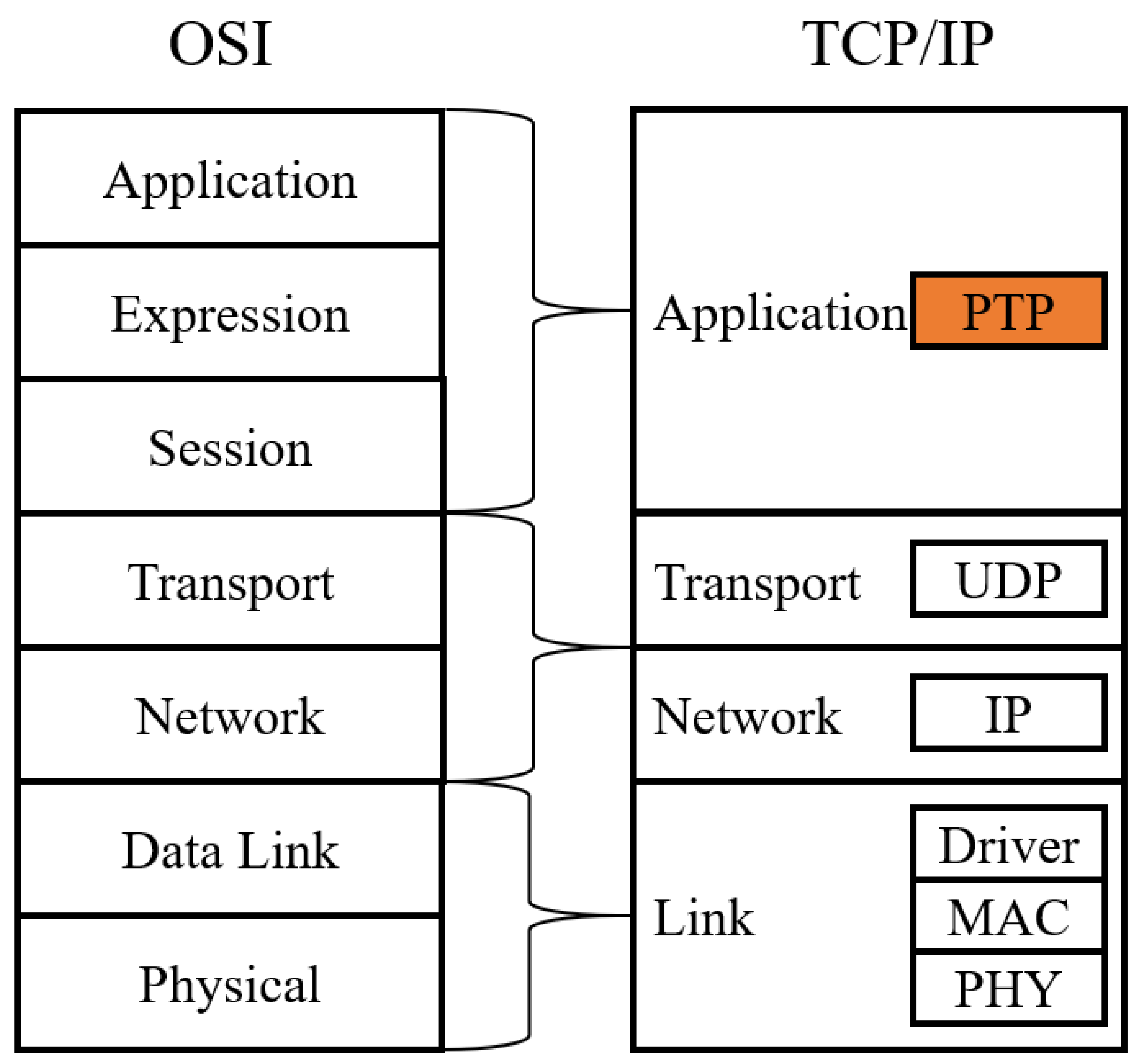
Figure 2 shows the network transmission protocol implemented by our system, which is formulated according to the simplified TCP/IP protocol [
10] of the OSI (Open System Interconnection) Model. The OSI model is to formulate seven-layer standards for software and hardware in the network and uses common standards to enable different systems to communicate with each other. The TCP/IP protocol is currently a widely used network transmission protocol for the merging of functional layers.
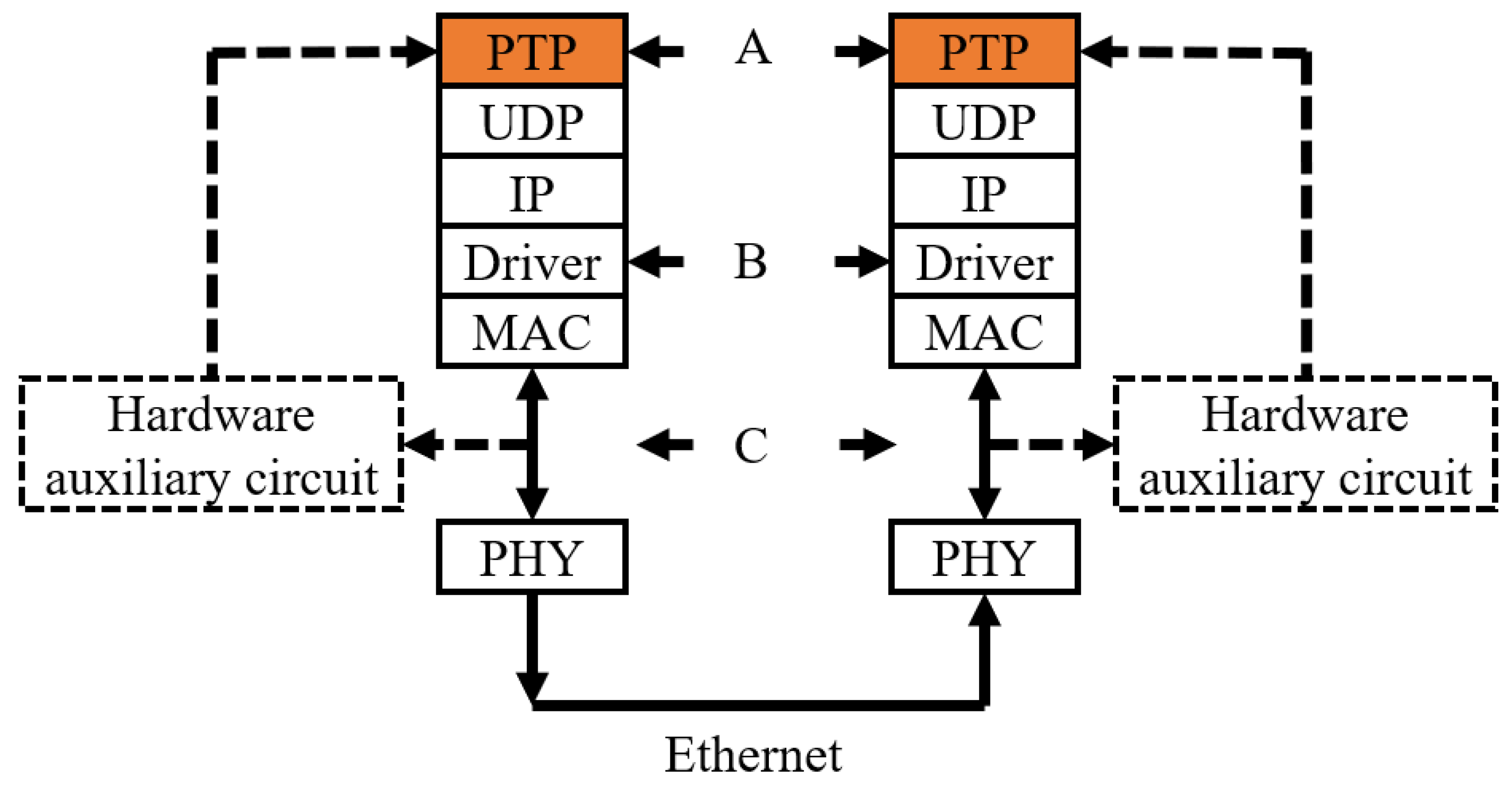
Figure 3 is the implementation architecture of the PTP protocol. In the agreement, points A, B, and C are the positions where timestamps may be generated [
11,
12]. The synchronization accuracy is greatly affected by the position where the timestamp is generated. Point A is at the application layer mark timestamp, this is the simplest way because it can be realized by software, but the jitter of the protocol stack delay is uncertain, and the delay jitter will cause a difference between about a few milliseconds ms and tens of microseconds μs due to errors, this implementation method is not used by ordinary people. Point B is to mark the timestamp between the network layer (IP layer) and the media access control layer (MAC layer). This method avoids the uncertainty of protocol stack delay jitter, and can also be implemented by software, and the time accuracy can reach the microsecond level. Point C is to mark the timestamp at the GMII (gigabit media-independent interface) close to the physical layer (PHY). GMII defines the logical and electrical characteristics of the reconciliation sublayer (RS) and gigabit media-independent interface (GMII) between CSMA/CD media access controllers and various PHYs. This method is based on the combination of software and hardware and requires the assistance of hardware auxiliary circuits. In the path that does not pass through the original packet to the application layer of PTP, due to the delay jitter of the physical layer is about the constant delay, which can provide sub-microsecond time precision. This section will introduce software time stamping and hardware time stamping, respectively.
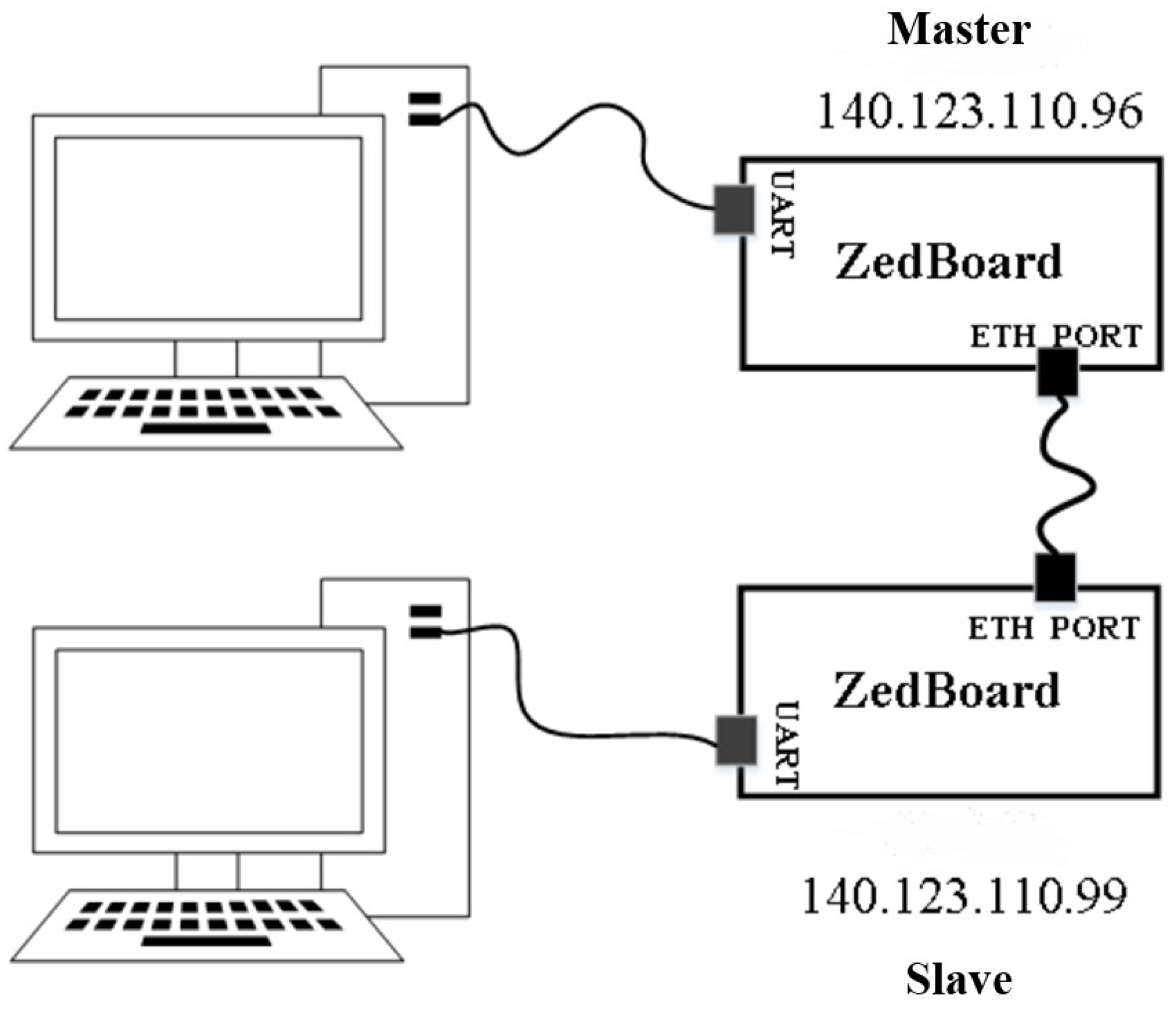
In the lab environment, two PCs are set up. The specifications are shown in
Table 1 and
Table 2. They are respectively used as the primary clock of the system and the secondary clock of the system. The network uses Ethernet to distribute fixed IP for connection and then uses the open source package software Linux PTP to realize. The software is implemented according to the IEEE 1588 protocol of Linux, provides a reliable implementation of the standard, and uses the application programming interface (API) provided by the Linux Kernel.
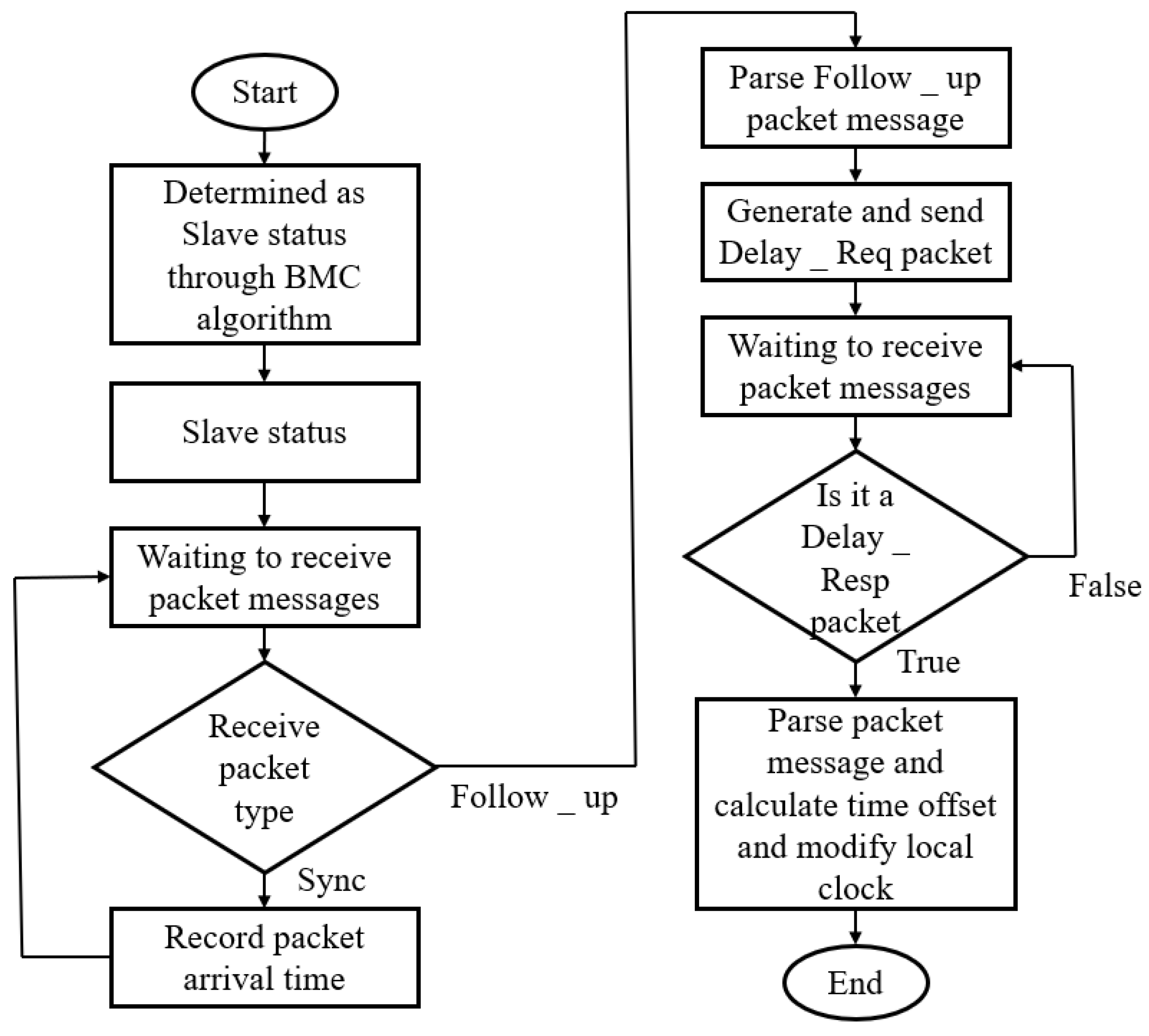
The actual execution flow of the system software is shown in
Figure 4 and
Figure 5.
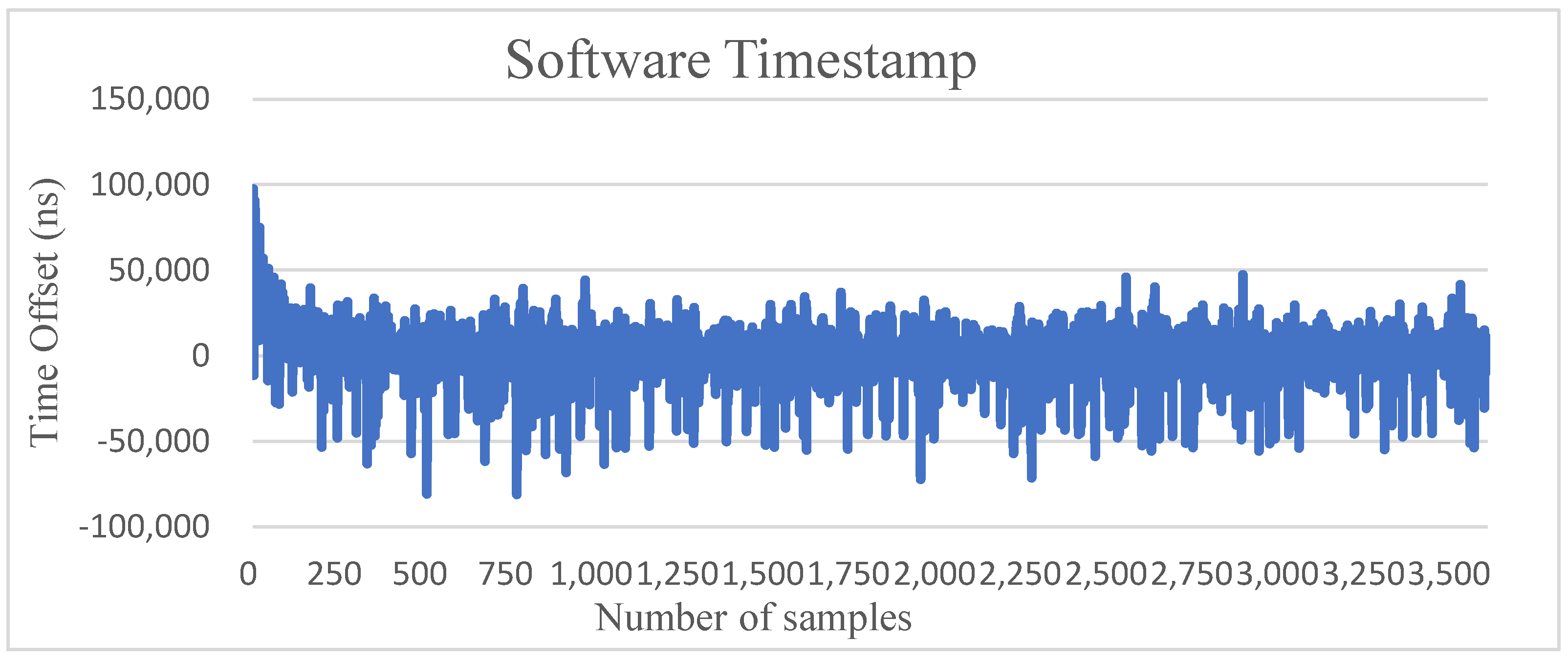
The experimental environment of our software timestamp is that the Primary transmits a synchronization packet to the Secondary every second.
Figure 6 shows the measurement results. After testing 3600 pieces of data for one hour, it can be seen that most of the measured values are concentrated in ±60 between microseconds.
In order to improve the accuracy of clock synchronization, it is necessary to make the timestamp closer to the physical interface, that is, the MAC or PHY layer, to reduce the impact of stack protocol delay [
13,
14,
15], also known as a hardware timestamp. The implementation of our hardware timestamp is shown in
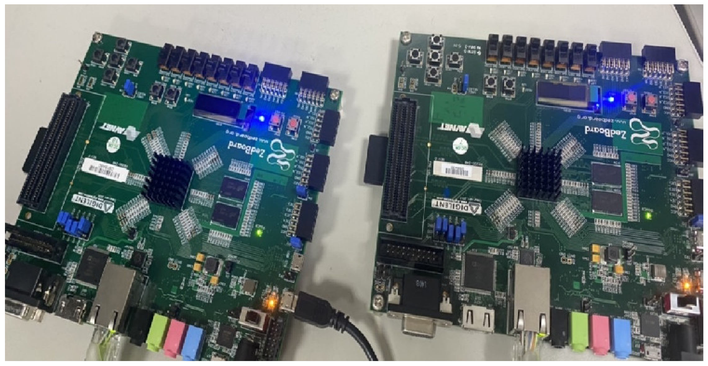
Figure 7. First, set up two ZedBoard development boards.
Table 3 shows the equipment specifications and the system software used. They are respectively used as the Primary and the Secondary of the system. The Ethernet is assigned a fixed IP for connection, and then the software package Linux PTP is also used for time synchronization.
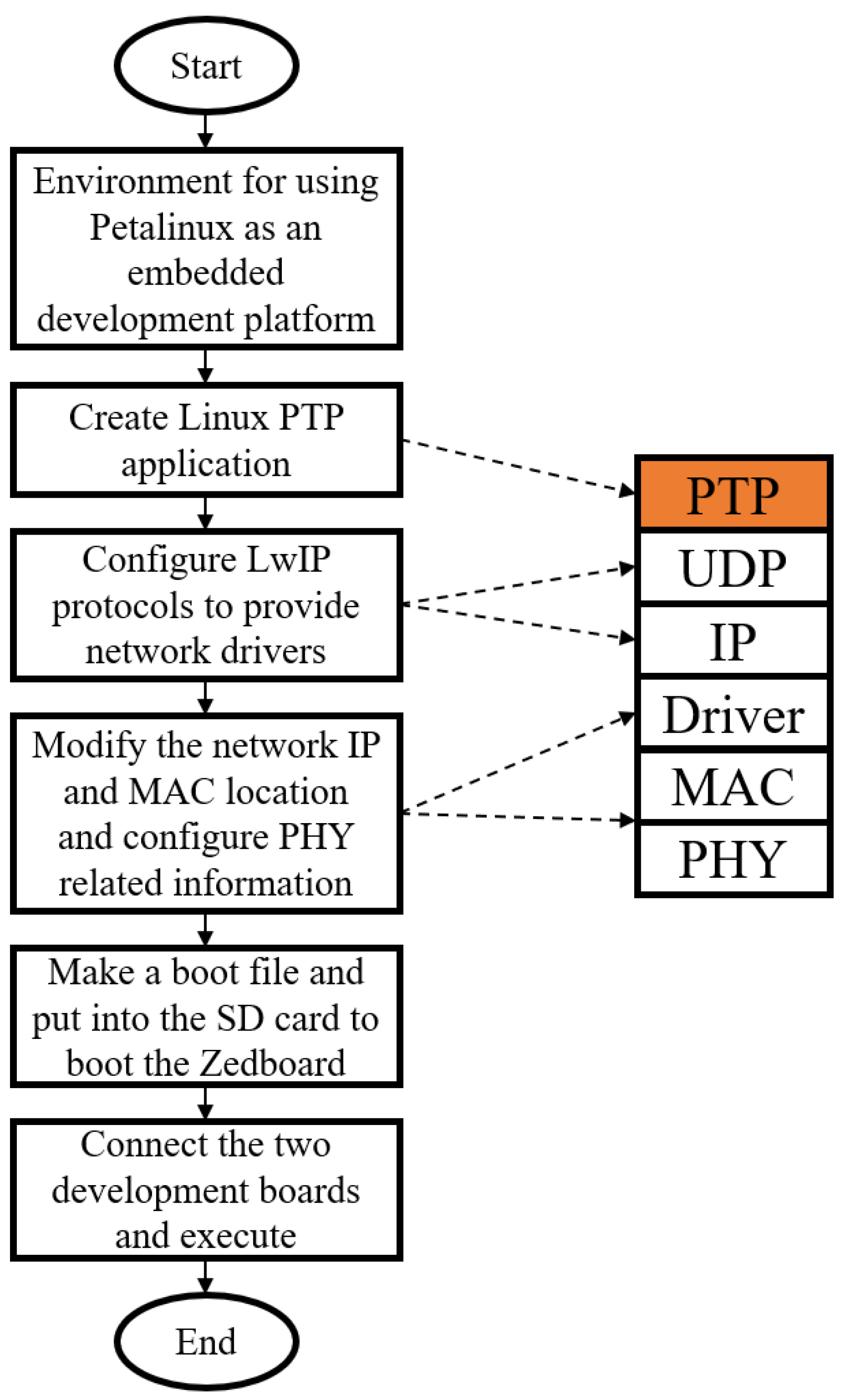
Figure 8 is a simple Zynq-embedded development board workflow chart. We want to build a development environment for an embedded platform of a Linux system with a package software Linux PTP, and the Petalinux platform is a tool developed by Xilinx for the Zynq-embedded Linux system, can run in the computer’s Linux (such as ubuntu) system environment and tailor-made execution files, and can be used together with Xilinx ISE hardware design tools [
16] to simplify the development process of Linux systems such as Zynq
®-7000 SOC and improve design efficiency. We use Petalinux 2017.4 and Petalinux 2020.2 for implementation.
Connect the two ZedBoard development boards with a network cable, make sure that the MAC and network IP of the two development boards are different, and run the PTP application, as shown in
Figure 9.
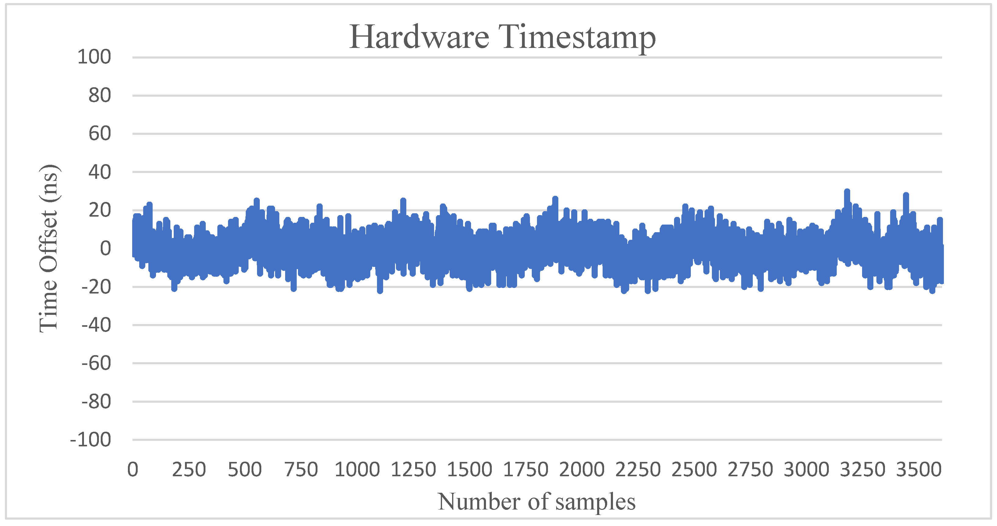
The experimental environment for our hardware timestamp is that the Primary sends a synchronization packet to the Secondary every second.
Figure 10 shows the measurement results. After testing 3600 records for one hour, it can be seen that most of the measured values are concentrated in between ±20 nanoseconds.
Based on the FPGA-based IEEE 1588 standard synchronization architecture [
17], we implemented a timestamp that can be captured between the PHY layer and the MAC layer, eliminating delay jitter caused by network protocol stacking, and thereby improving synchronization accuracy. When the Primary and Secondary are connected through a network cable, the deviation of IEEE 1588 clock synchronization can be limited to ±20 ns. Compared with the related research in
Table 4, the realization results of this article have high clock synchronization accuracy.
From the above practice and related research, it is found that in order to improve the accuracy, the congenital frequency error between the oscillators must be considered. An IEEE 1588 auxiliary timestamp with dynamic frequency compensation is also proposed; it is designed as a chip to reduce the delay of protocol stacking and to improve the accuracy of time so that it can be applied to more needs.
4. IC Design and Implementation of PTP Hardware-Assisted Timestamp
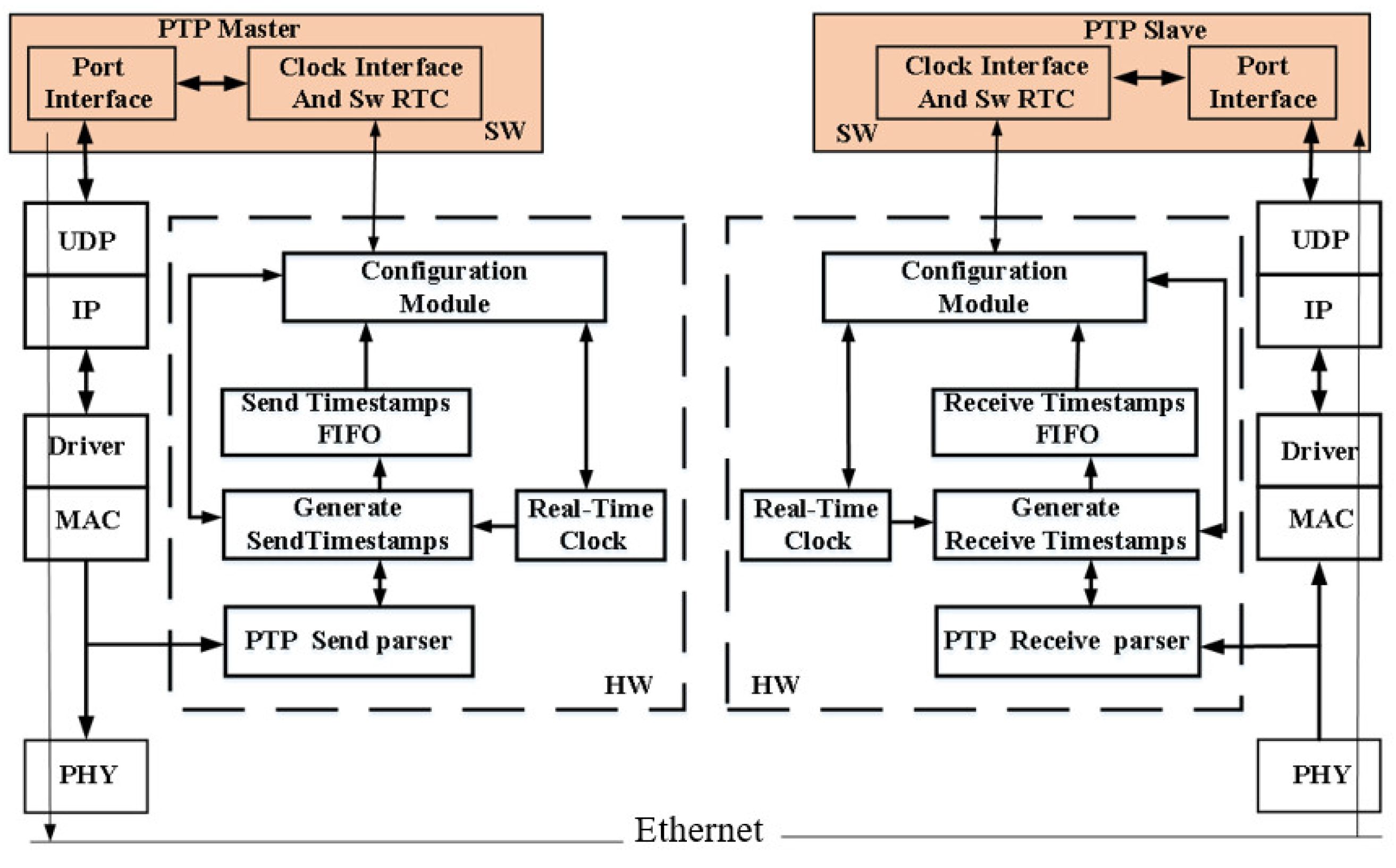
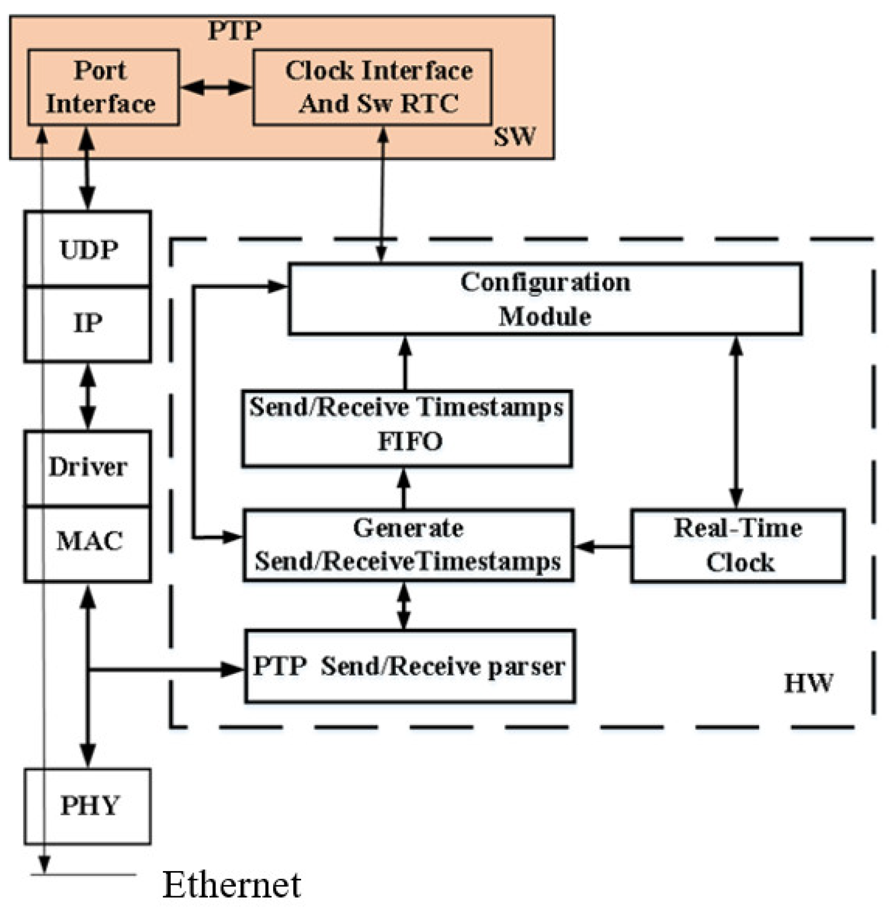
Figure 11 is our system architecture diagram, taking Primary sending packets to Secondary as an example. The CPU software (SW) acts as the processing core, manages the synchronization process in the hardware, calculates the time offset, and adjusts the hardware’s real-time clock. The hardware is located in the gigabit media-independent interface (GMII) between the MAC layer and the PHY layer. GMII can be used to detect the information of each packet on the interface and communicate with control signals.
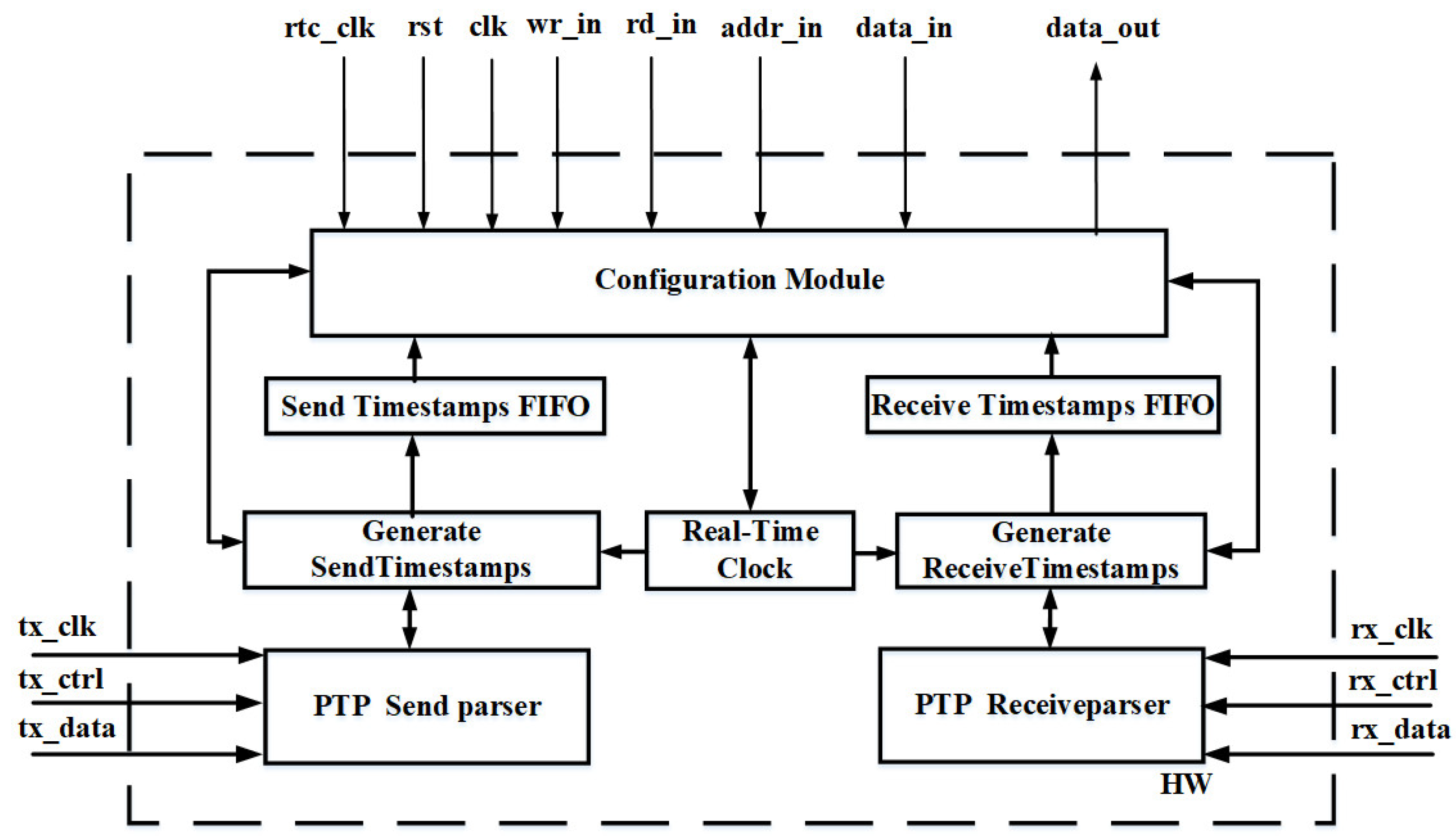
Figure 12 is our Block Diagram. The hardware part completes the frequency-adjustable real-time clock (Real-Time Clock), the parser (Parser) of the PTP packets at the receiving end (Receive) and sending end (Send), and the generation of timestamp (Generate timestamps) at the receiving end (Receive) and sending end (Send), and write the timestamp with the control signal into FIFO (First In, First Out). If the control signal is recorded, write the recorded timestamp to the output, and update the corresponding control signal; otherwise, the timestamp will be discarded. The I/O pin assignment is shown in
Table 5.
The hardware-assisted timestamp is mainly divided into two blocks: the receiver (Receive) and the sender (Send), and use the PTP parser (Parser) with the real-time clock to generate the time stamp, respectively, and store the timestamp in the FIFO register. In the process, the PTP configuration register (Configuration Module) is updated through the control signal, so that the software end can obtain the timestamp. Next, we will describe the design of the hardware, as shown in
Figure 13.
The Configuration Module is a register that stores the timestamp of the PTP message and other Module-related parameters. The main structure is a multiplexer. Input the 32-bit data_in and 8-bit addr_in as the relevant parameter address of the synchronization node, and input them in series. Input 40-bit period_comp and 40-bit adj comp as dynamic frequency compensation parameters, which are mainly obtained from PTP parser Module and Generate timestamps Module, and tx_data_in and rx_data_in are two packets of information obtained between the MAC layer and the PHY layer because the total length of the packet is long and not fixed, so 8-bit serial input is used to reduce the number of IO Pads. The output is data_out that is combined with other Module-related parameters and timestamps. Since the original output data_out pins are as many as 256, it will cause a serious pad limit. Therefore, 32-bit serial output is used to reduce the number of IO Pads, as shown in
Figure 14.
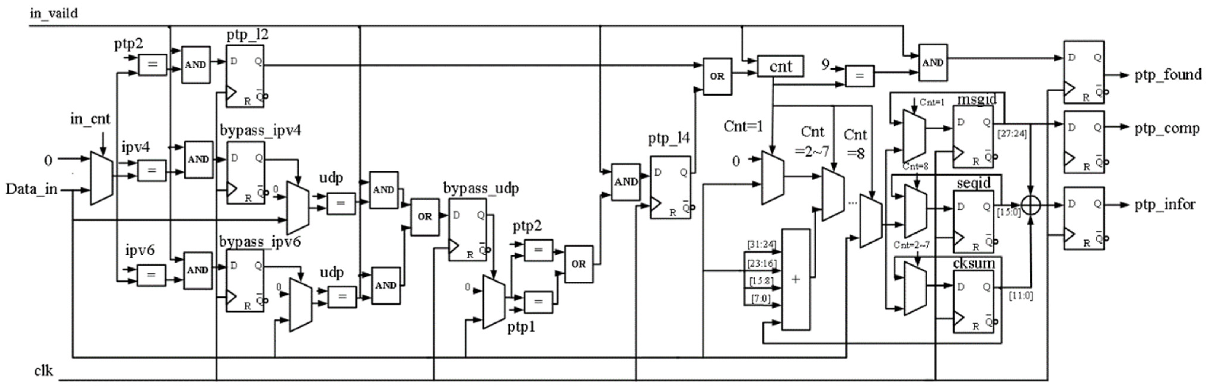
A PTP parser is a module used to parse whether the received packet is a PTP packet message. Its main structure is a comparator, as shown in
Figure 15. The input Data_in is the packet information obtained between the MAC layer and the PHY layer and is serially input, and the multiplexer and the cnt counter are used to obtain the information used to judge the message header. In the information segment, whether it is a PTP packet is determined by identifying the message header layer by layer, and the output ptp_infor is a 32-bit PTP packet identification. ptp_found records whether it is a PTP packet, which will be sent to the FIFO Module for use. ptp_comp analyzes whether the packet is a Sync and Follow_up packet, and sends this signal to the Configuration Module for use.
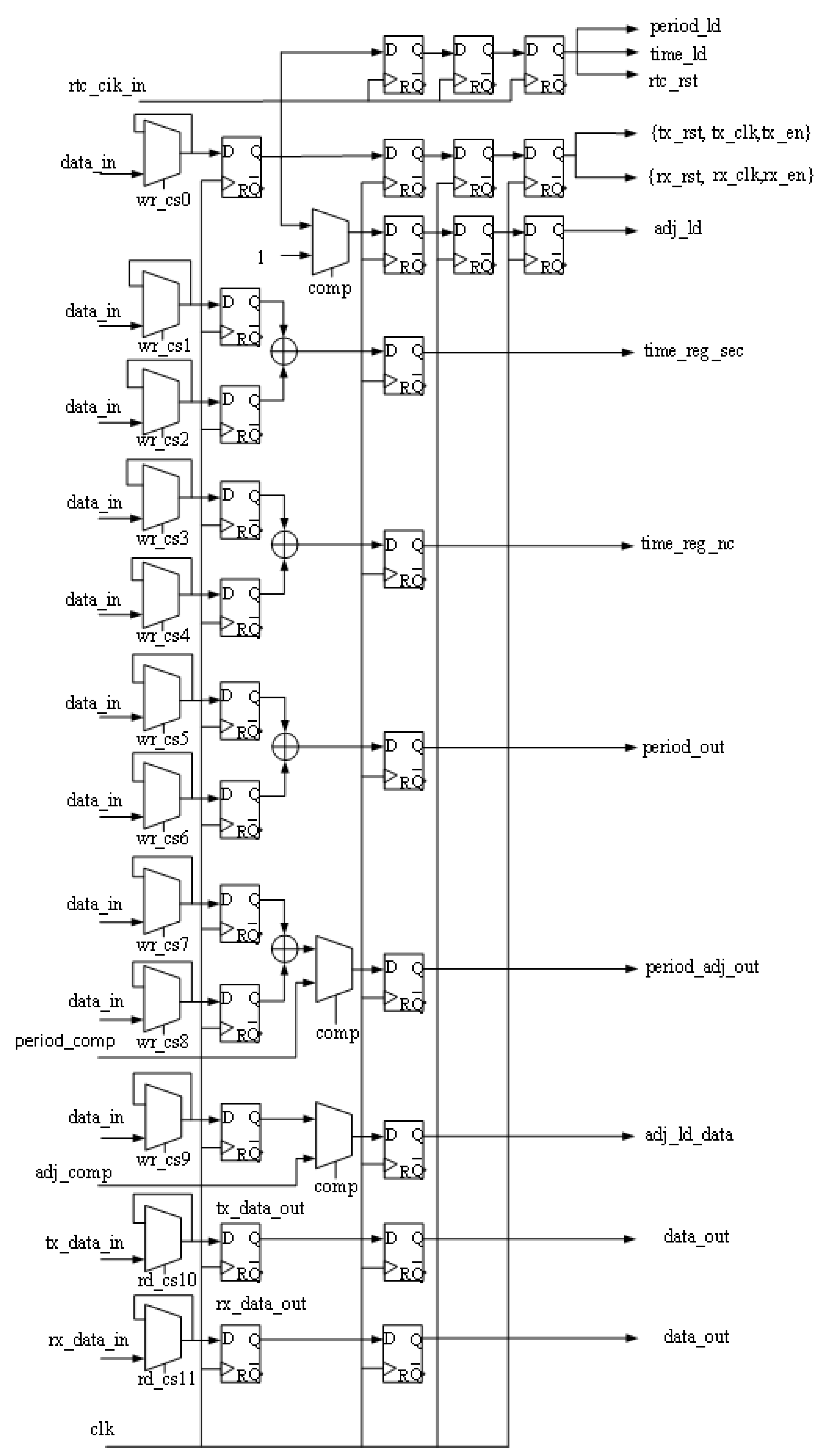
The function of Real-Time Clock is to generate a real-time clock with adjustable frequency. The architecture of the real-time clock is shown in
Figure 16. The input and output time accumulators adopt the PTP protocol standard: 48-bit second field, 32-bit nanosecond field, and add an 8-bit sub-nanosecond (sub-ns) field to improve clock accuracy. The input period_in is composed of 40-bit temporary registers, of which 8 bits record nanoseconds, and the last 32 bits record sub-nanometers. The main function is to accumulate each oscillation of the oscillator in the free-running mode of the system; for an example such as a reference clock for a frequency of 125 MHz, add 8 nanoseconds to each oscillation. The clock is usually implemented using a counter register, driven by a quartz crystal oscillator. The disadvantages of these oscillators are low accuracy, susceptibility to environmental influences, low long-term stability, and non-adjustable frequency. The frequency of the crystal changes over time and as the ambient temperature changes. With the help of frequency compensation technology, the crystal frequency can be dynamically compensated to keep the frequency at a stable value. Crystals with relatively poor performance can also be successfully used in high-precision clock synchronization systems. The frequency is compensated by initiating the time adjustment step by writing the period adjustment and period count to the period_adj and adj_cnt registers, respectively. The period adjustment is in nanoseconds ns, with 8 integer bits and 32 decimal bits. Since the input time accumulator is 8-bit sub-nanoseconds, the resolution is 2
−8 nanoseconds and the register of the oscillator is 32-bit sub-nanoseconds, which means the resolution is 2
−32 nanoseconds, so when the accumulated value of the oscillator is not an integer of 2
−8, use a temporary register to save its decimal place and count it in a loop. This method can improve the precision of the clock.
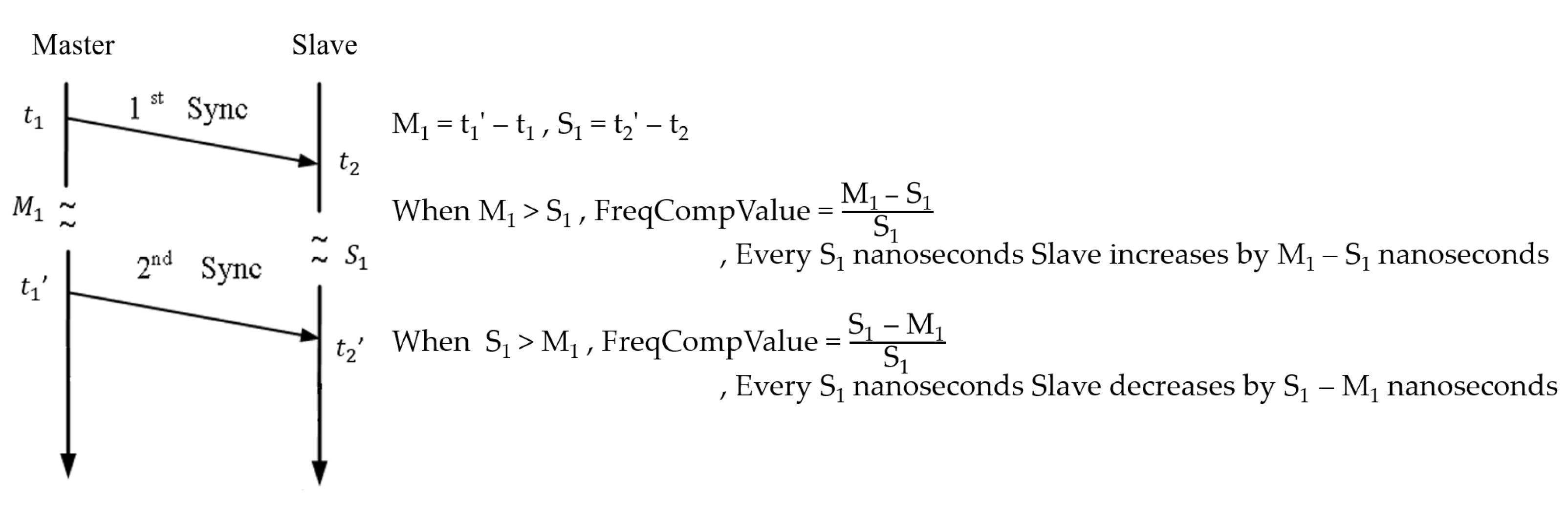
Figure 17 shows the dynamic frequency compensation Frequency compensation [
20,
21,
22] used in this article. The PTP Primary will periodically send a synchronization packet to the PTP Secondary, record the sending time t
1, t
1′ and the receiving time t
2, t
2′ in the temporary register, and use a 32-bit count temporary register to calculate the compensated frequency, and calculate the compensated value FreqCompValue to compensate the Secondary clock.
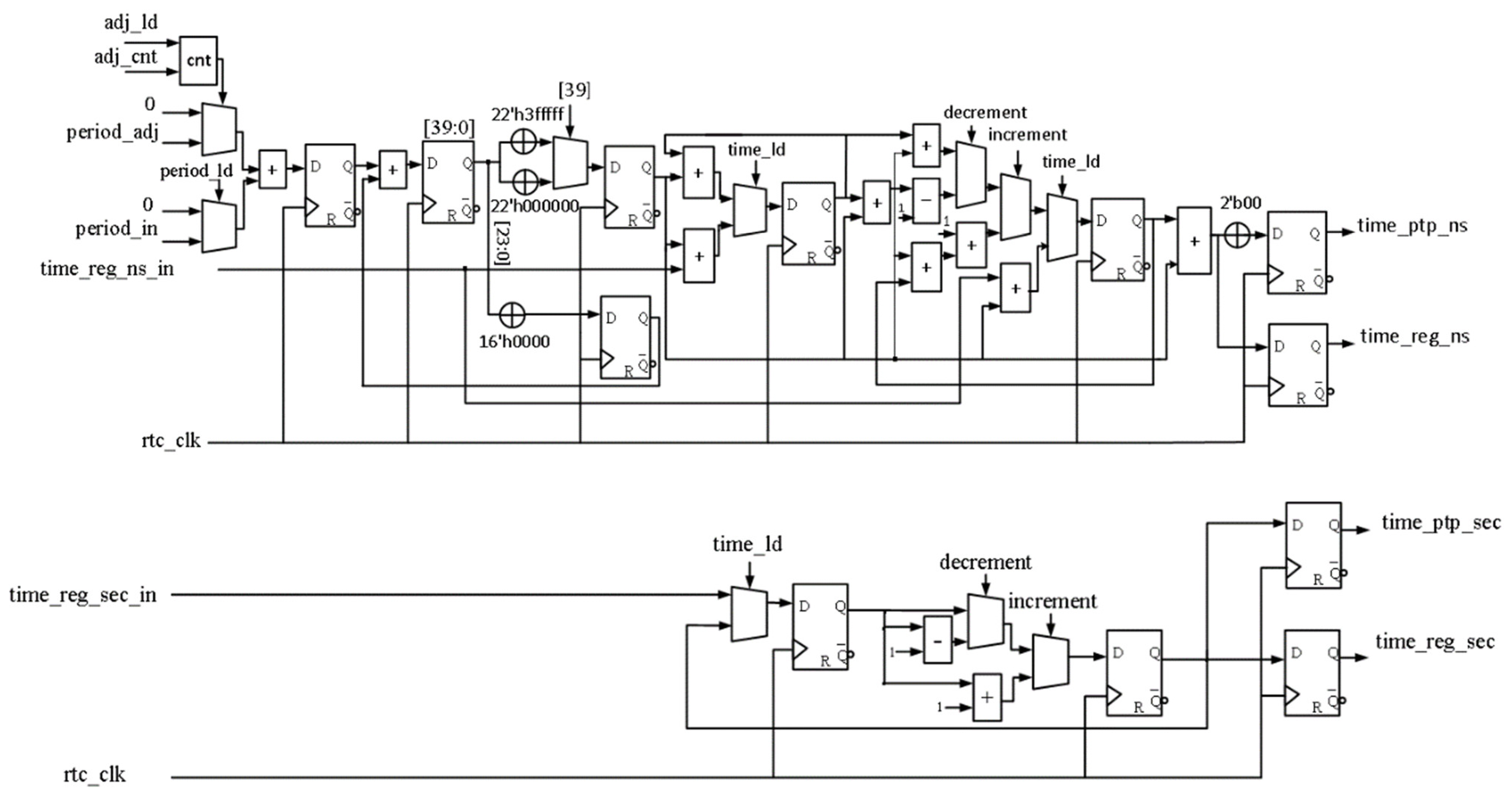
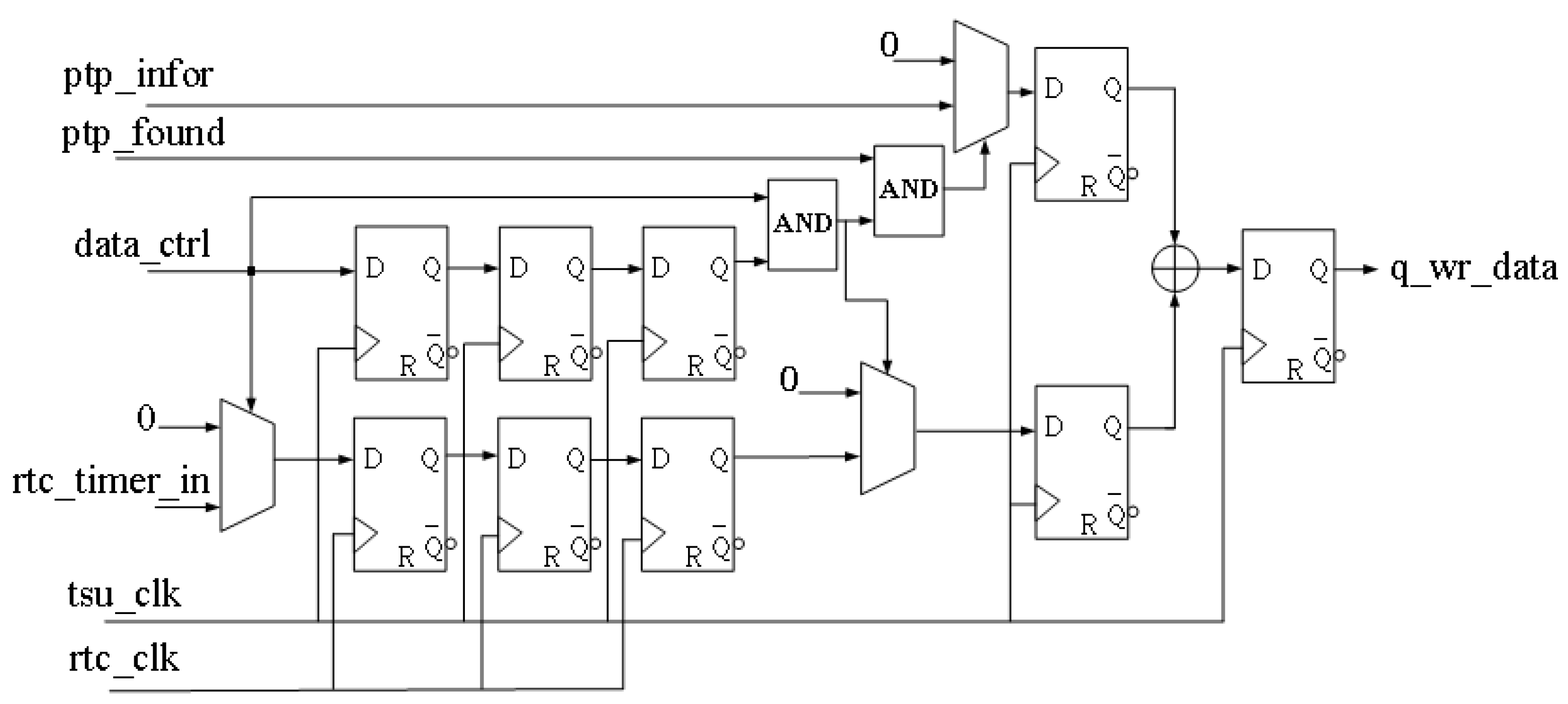
The Generate Timestamps Module is shown in
Figure 18. It combines the information in the above-mentioned module register to form a timestamp. The timestamp [
23] is composed of 110 bits, which includes 80-bit time information and 30-bit PTP Packet identification, and store this data in FIFO, using the control signal generated from the parser to indicate whether to generate a timestamp. In order to avoid the problem of metastable state when sending relevant parameters to the corresponding registers, two DFF registers and a hand-shaking protocol are added to trigger the action, so that the output can obtain the correct control signal or Packet information.
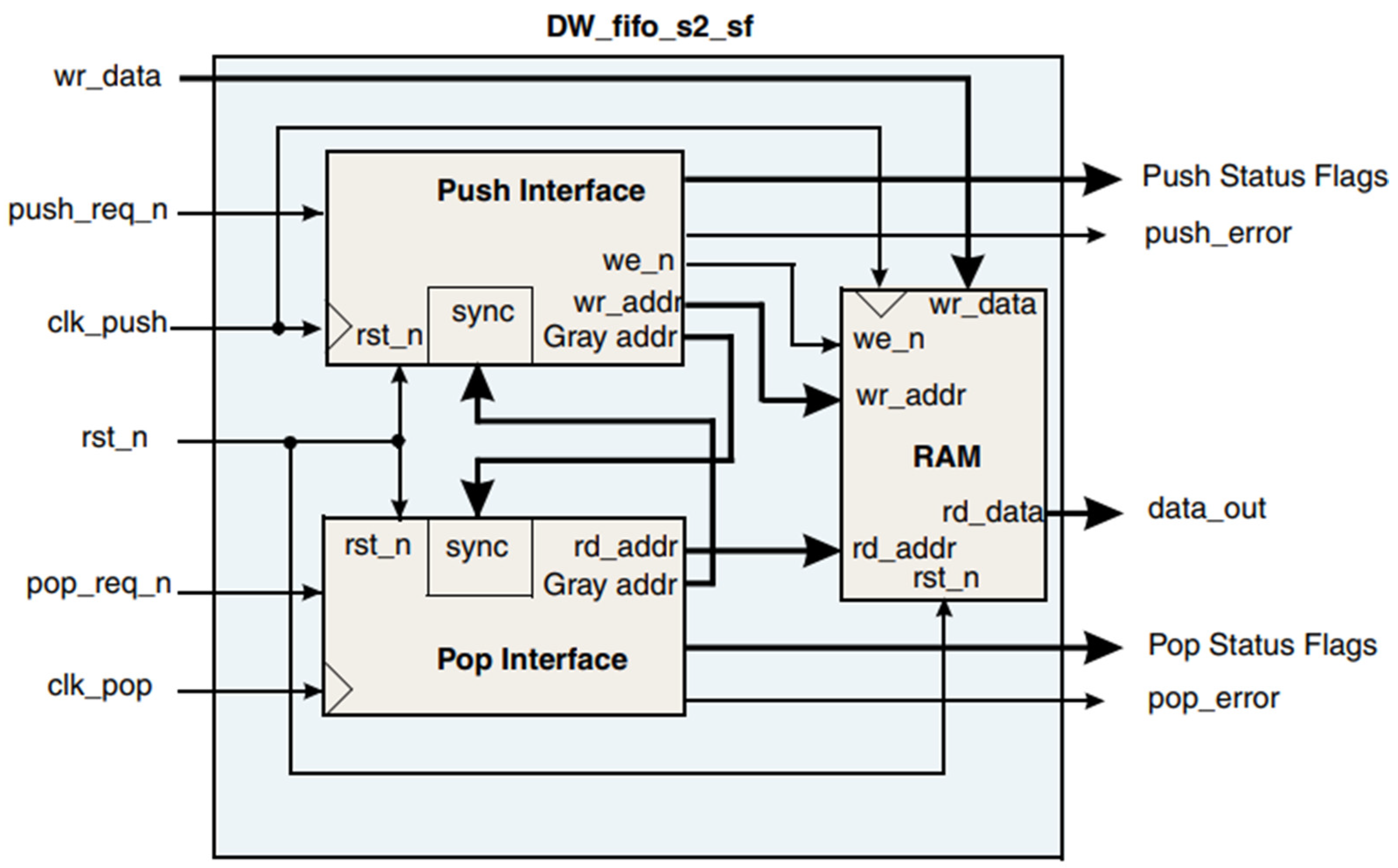
We use the IP provided by Synopsys, as shown in
Figure 19; the reading and writing work under their respective clocks, and the writing clock will match the control signal to write the data into the FIFO. FIFO contains dual-port RAM (random access memory), which can read and write at the same time. When writing, wr_addr starts from 0; every time a piece of data is written wr_addr increases by one and points to the next storage unit. When the FIFO push_full is full, the data will no longer be written; otherwise, the previous data will be overwritten and the data will be lost. The read clock will be matched with the control signal to read the data from the FIFO. When reading, rd_addr starts from 0; every time a piece of data is read, rd_addr increases by one, and points to the next storage unit. When the FIFO pop_empty is empty, the data can no longer be read; otherwise, the read data will be wrong data.
5. Experimental Results and Analysis
We use Faraday’s 0.18 μm and TSMC’s 45 nm ARM standard component libraries to design and implement, and Gate_count is based on 2-input NAND to calculate the approximate number of logic gates used. The results of the synthesis experiments are compared in
Table 6.
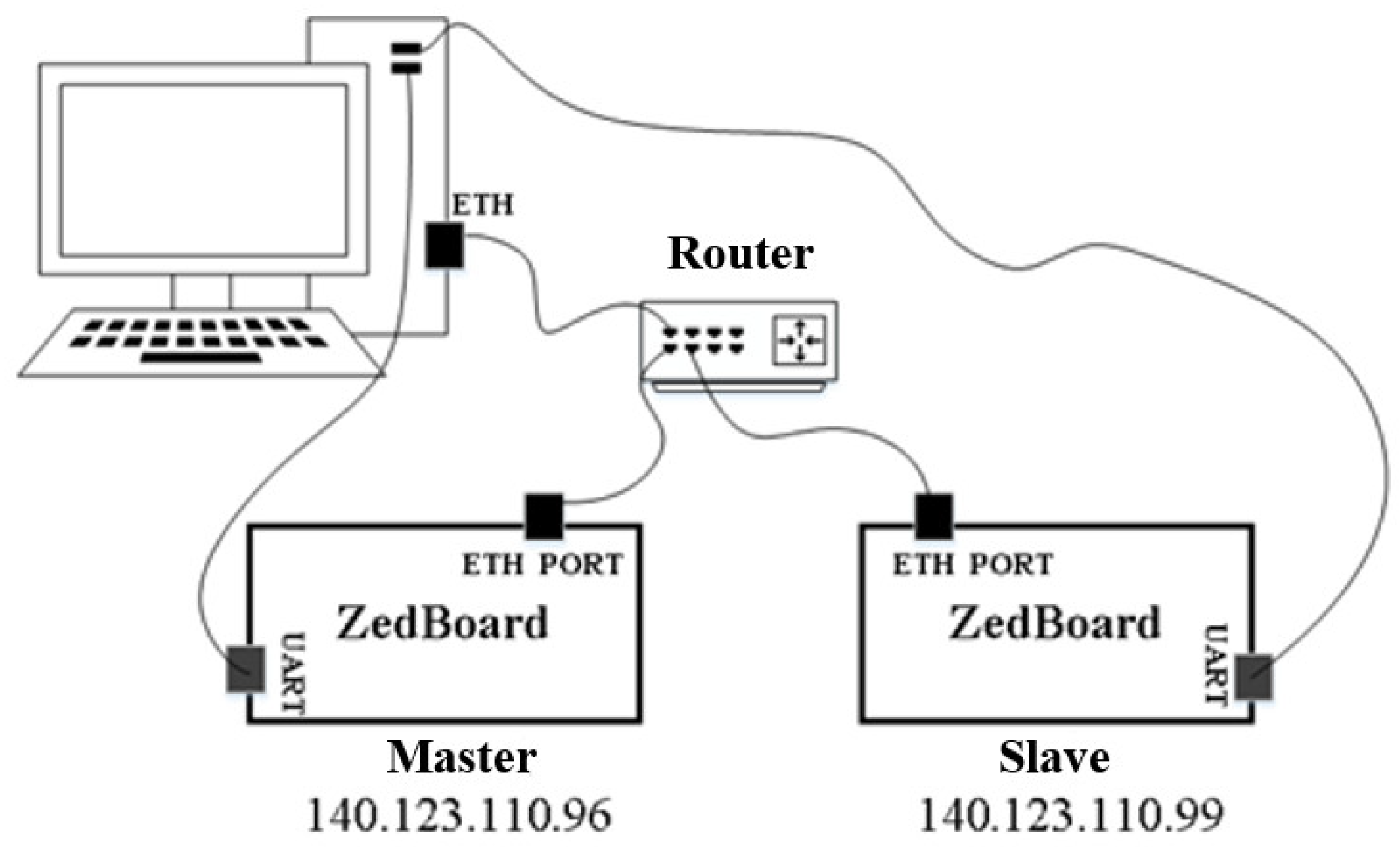
Our test pattern is implemented through the hardware timestamp mentioned above. Two Zedboard development boards and a PC are connected to a general router through a network cable, as shown in
Figure 20, and the packet is captured through the software Wireshark. Then, you can extract PTP-related packets, and use the contents of the packets as a test pattern for hardware circuit simulation.
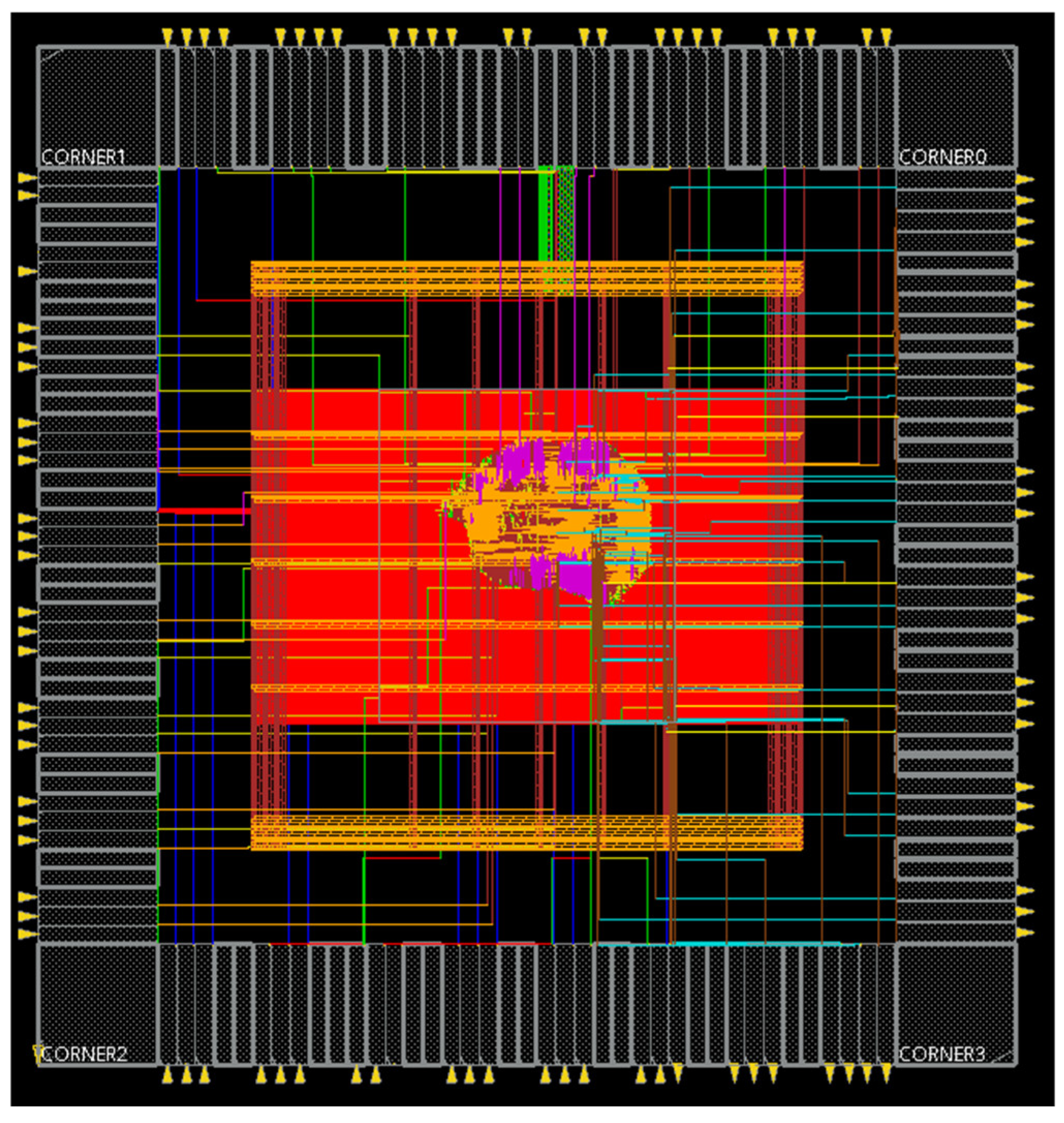
Our IC layout is shown in
Figure 21, and the chip specifications are shown in
Table 7.
We have implemented three kinds of timestamps, and their comparison is shown in
Table 8. It can be seen that the offset of the software timestamp is the largest, which also means that its error is the largest.
6. Conclusions
In this paper, based on the detailed analysis of the PTP protocol, we first use the Ethernet network and fixed IP address for connection, and then use the open source software package Linux PTP for measurement. Its software timestamp is 60 microseconds. Then, we build a clock synchronization system using FPGA to match the PTP protocol. On the Xilinx Zynq-7000 SOC platform of Petalinux, a hardware solution based on the IEEE1588 protocol in the Linux PTP application is implemented. The experimental results show that the implementation results have high clock synchronization accuracy, and the hardware timestamp is 20 nanoseconds. Compared with related implementations, this design improves the time synchronization accuracy, simplifies the hardware circuit design, greatly reduces the development cost and difficulty, and has excellent portability and scalability, which provides a certain reference value for future research.
After matching the implementation of the FPGA and the PTP protocol in this paper, it is found that in order to improve the accuracy, the congenital frequency error between the oscillators must be considered. An IEEE 1588 auxiliary time stamp with dynamic frequency compensation is also proposed; it is designed as a chip and can operate at 370 MHz under 45 nm (TN40G), uses four-cycle serial output, and the Latency is 10.8 (2.7 × 4) ns resolution, which reduces the delay of the protocol stack and improves the accuracy of the time, so that it can be applied on more demand.
This thesis designs PTP auxiliary time stamps and completes the realization of detecting PTP packet messages and recording time stamps. However, in order to verify the complete PTP system clock synchronization function, it is necessary to use a software processor as the processing core and use the ARM platform of the Linux system. The synchronization process in the FPGA is managed, offsets are calculated, hardware clocks are adjusted, etc. If the system can be integrated to complete the SOC single chip with the complete functions of the PTP protocol, the implementation cost and volume can be reduced, making it beneficial to be applied to more industrial Internet of things devices.


