Article

Wideband Circularly Polarized Magneto-Electric Dipole Antenna Array with Metallic Walls for Millimeter-Wave Applications

1
Beijing Key Laboratory of Millimeter Wave and Terahertz Technology, School of Integrated Circuits and Electronics, Beijing Institute of Technology, Beijing 100081, China
2
Tangshan Research Institute, Beijing Institute of Technology, Tangshan 063099, China
*
Author to whom correspondence should be addressed.
Electronics 2023, 12(10), 2154; https://doi.org/10.3390/electronics12102154
Submission received: 27 March 2023 / Revised: 3 May 2023 / Accepted: 7 May 2023 / Published: 9 May 2023
(This article belongs to the Special Issue Recent Advances in Microwave Engineering: Design and Application)

Abstract

:
This work proposes a new circularly polarized (CP) 4 × 4 magneto-electric (ME) dipole antenna array using metallic walls for 28 GHz band applications. The ME dipole element is surrounded by eight metallic walls and is excited fed by microstrip line. By introducing metallic walls, the 3-dB axial ratio (AR) bandwidth of the element is increased from 23% to 36.5%. The 4 × 4 array is fed by a simple 1-to-16 microstrip power divider. In contrast to the conventional substrate integrated waveguide (SIW) power divider using two layers, the proposed microstrip divider only needs one substrate layer. The experimental 3-dB AR bandwidth of the array achieves 30.1%, ranging from 22.5 to 30.5 GHz, which falls inside the −10 dB impendence bandwidth. The measured maximum gain is 19.2 dBic.

1. Introduction

Millimeter-wave (mm-wave) band attracts increasing interests in 5G and satellite communications due to its merit of wide bandwidth [1,2]. To compensate for path-loss, a high-gain antenna array is essential [3]. On the other hand, circular polarization is preferred because it has the merits of multipath interference suppression and no polarization alignment loss [4]. It is rewarding to design a mm-wave CP antenna array that has features such as a wide bandwidth, excellent gain, and simple structure.
Over the previous decades, many wideband CP elements have been presented for array designs [5,6,7,8,9,10,11,12,13,14,15,16,17,18,19,20,21]. Stacked patch [5,6,7], ME dipole [8,9], curl antenna [10,11,12], spiral antenna [13,14], cavity antenna [15,16,17], slot antenna [18], and dielectric resonator antenna [19,20,21] are the popular elements. For example, in [6], a wideband circularly polarized radiation is generated owing to the combination of a pair of shorted pins with four identical square patches, and the 3-dB AR bandwidth of the stacked patch array achieves 25.4%. In [9], by truncating several corners and adding L-shaped branches into the ME dipole element, 3-dB AR bandwidths of the element and the 4 × 4 array are 17.3% and 16%, respectively. In [18], a differentially fed slot antenna contains 20.4% AR bandwidth, whereas the 4 × 4 array possesses a bandwidth of 33.6%. However, among the above-mentioned designs, some arrays have a relatively narrow bandwidth, while others require more substrate layers or a high profile. Another way to increase the AR bandwidth is utilizing the sequentially rotated (SR) feeding technique [22,23,24,25,26,27,28,29]. For instance, a 2 × 2 subarray with 17% AR bandwidth is proposed in [22], with each element fed by equal amplitude and phase signals. Through an H-shaped SIW SR feeding network, the four subarrays’ excitation signals have a 90° phase difference from one another, thus expanding the bandwidth of the 4 × 4 antenna array to 27.8%. In [25], the element’s AR bandwidth is 23.8%, and that of the 2 × 2 array is 30% because of the utilization of a microstrip SR feeding structure. However, the SR feeding structure increases the complexity of the antenna.
Recently, Pan et al. proposed the method of using vertical metallic walls to improve the AR bandwidth of antennas [30,31,32]. The metallic walls are sequentially placed at each edge of the ground planes, working as parasitic radiators. For example, a cross dipole antenna working at 2 GHz is put forward in [30]. The AR bandwidth is extended from 30% to 130% by utilizing four vertical metallic plates. Similarly, a dielectric resonator antenna with vertical metallic plates is studied in [31]. Because the orthogonal current is coupled to the metal plates, an AR bandwidth of 49.5% is obtained. However, these antennas have 3D structures and are designed in low frequency regime. Furthermore, all the designs in [30,31,32] only focus on a single antenna prototype. The array prototype with metallic walls is yet to be developed.
On the other hand, to minimize the profile of CP array or the number of substrate layers, it is an effective method to choose microstrip lines as excitation structures [6,9,26]. A SIW structure can also be used as an antenna excitation. In spite of the fact that the array based on SIW feed technology in [11] only uses two dielectric substrate layers, it suffers from a narrow operating bandwidth. Some CP array designs use multiple substrate layers to enhance the bandwidth of the array [8,22,33,34,35]. In [33], a SIW feeding network consists of two layers of substrate, and the 4 × 4 patch antenna array achieves 23.8% bandwidth. However, the assembly process becomes more complicated and more expensive, which limits the application of the arrays for commercial purposes.
In this study, a compact wideband CP ME dipole antenna array with vertical metallic walls is proposed at 28 GHz band. Firstly, the ME dipole element in [36] is modified. The SIW feeding network is replaced by microstrip line to reduce the number of substrate layers. Then, eight vertical metallic walls are placed around the ME dipole to improve the AR bandwidth, which can be fabricated through the PCB technique. Finally, the dimensions of the walls are optimized in a 4 × 4 array. The practical test results indicate that the overlapping impedance and AR bandwidth achieves 30.1%, and the array has only two substrate layers. To the best of our knowledge, this is the first time that vertical metallic walls are explored to increase the bandwidth of a CP array in the mm-wave band.

2. Antenna Design

2.1. Configuration of the CP Element

Figure 1 displays the configuration of the CP element. Figure 1a observes that two pieces of substrate are tightly stacked. The thickness of substrate1 is 1.27 mm, and the material is TMM3 (εr = 3.45, tan δ = 0.002). The thickness of substrate2 is 0.203 mm, and the material is RO4003C (εr = 3.55, tan δ = 0.003). Figure 1b depicts the top metallic layer of the element. It is composed of a ME dipole and eight vertical metallic plates. The plates are fabricated by using vias and metallic strips. As shown in Figure 1c, the bottom of substrate2 has a microstrip line printed on it. Electromagnetic energy is coupled from the microstrip line to the ME dipole through the slot carved on the ground plane of the center metallic layer.
The choice of dimensions is discussed. Firstly, the dimensions of the crossed ME dipole are determined. As we know, each arm of the ME dipole is about a quarter wavelength in substrate. It means that L1 and L2 should be around 2 mm. Then, the dimensions of the coupling slot on the ground are selected. The slot is used to couple energy to the ME dipole, because by itself, it does not radiate energy. Therefore, the length of the slot should be less than half-wavelength in substrate, which is chosen as 3 mm. Then, the dimensions of the vertical metal plates are determined. The metal plates work as parasitic directors. Therefore, the length for the metal walls also needs to be shorter than half-wavelength in substrate, which is chosen as 2.9 mm. Based on these initial values, the detailed dimensions are carefully optimized by full-wave simulation software Ansoft HFSS ver. 2018. Table 1 displays the optimal dimensions for the element.

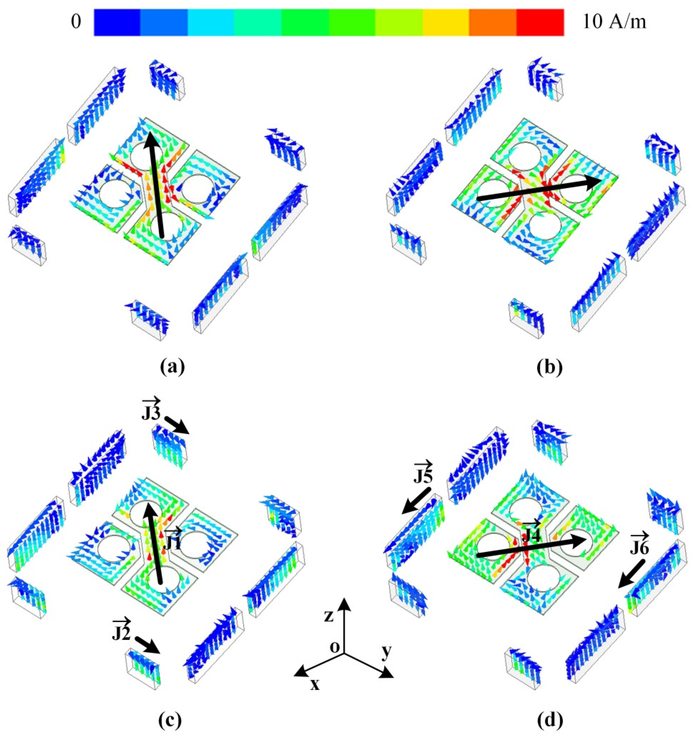
2.2. Working Mechanism of the CP Element

Compared to other kinds of antennas, an ME dipole has low profile, excellent antenna performance, such as a good impedance bandwidth, stable gain, and desirable radiation front-to-back ratio, making it ideal for mm-wave application. Therefore, many CP arrays based on an ME dipole have been proposed in the mm-wave band [8,9,22,36]. In [22], an ME dipole antenna fed by a SIW to coaxial transition structure has −10 dB impedance bandwidth of 24.2% and a 3-dB AR bandwidth of 16.5%. In addition, an aperture-coupled ME dipole achieves a bandwidth of 25.9% [36]. In this design, the method of vertical metal walls is applied to the element in [36] to further expand its bandwidth. The design process of the proposed element is illustrated in Figure 2. As seen in Figure 2, Type is a traditional ME dipole fed by SIW. The performance of Type I is described in detail in [36]; the impedance bandwidth is 28.8%, and the AR bandwidth is 25.9%. To minimize the number of substrate layers of the antenna array, the SIW Excitation structure is replaced by a microstrip line in Type II. Next, in Type III, eight vertical metal walls are added around Type II for enhancing the bandwidth of the element. To fabricate the antenna through PCB technology, the metallic walls are replaced by vias and metallic strips in Type IV. For comparison, the EM dipole is the same size in all models, as shown in Table 1 in Section 2.1.
Figure 3a,b depict the elements’ simulated reflection coefficient and AR performance. It is shown that the impedance and AR bandwidth of Type II is 34.9% (24.8 GHz to 35.3 GHz) and 23% (23.8 GHz to 30 GHz), respectively, which is close to the performance of Type I. This indicates that the microstrip line can replace the SIW structure for feeding without affecting the performance of the element. When the vertical metallic walls are introduced, both the impedance bandwidth and AR bandwidth are significantly improved. Additional resonance is observed in the upper frequency band, which is expected to be attributed to the vertical metallic walls. Compared with Type II, the impedance bandwidth of Type III is increased from 34.9% to 44.5% (22.7 to 35.7 GHz) and the AR bandwidth is increased from 23% to 36.5% (23.3 to 33.7 GHz). The performances of Type IV are similar with those of Type III. It means that using vias and metallic strips to replace the metallic walls has little influence on the performances.
To further study the working mechanism of the ME dipole surrounded by vertical metallic walls, the currents distributed on the antenna are exhibited at two frequency points, as depicted in Figure 4. At 26 GHz, strong currents are observed on the ME dipole, whereas weak currents are on the vertical metallic walls. It means that the ME dipole is the main radiator at 26 GHz. The directions of currents at t = 0° and t = 90° are orthogonal in space, and the amplitudes are close. Therefore, CP fields at 26 GHz are generated by the ME dipole and the vertical metallic walls have negligible effect. At 32 GHz, the currents are strong at both the ME dipole and metallic walls. It indicates that the parasitic walls are also effective radiators at 32 GHz, which provide additional degrees of freedom for good AR performance. Observed from the currents at T = 0° and T = 90°, it is known that the CP wave is generated at 32 GHz.

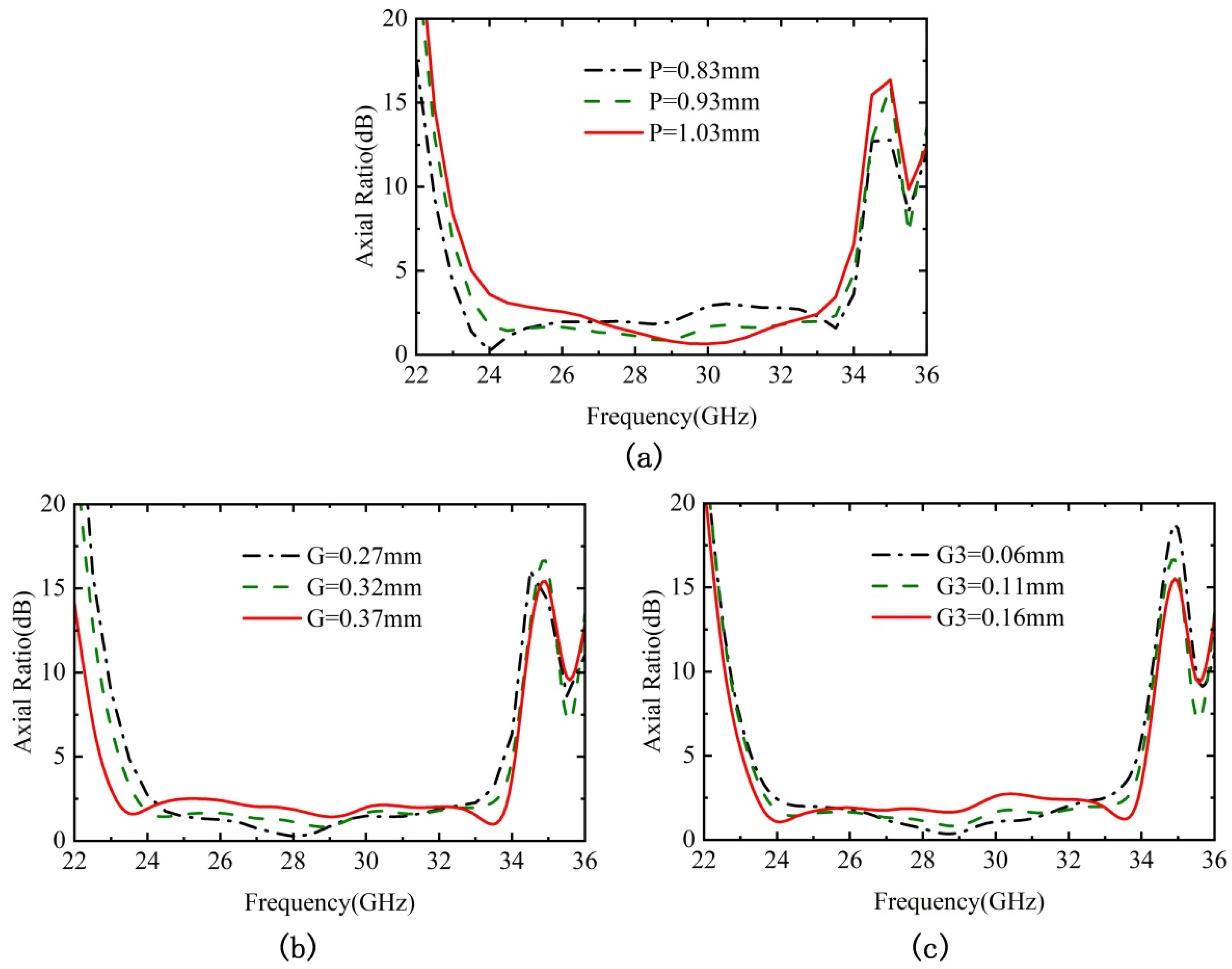
2.3. Parameter Analysis of the CP Element

To guide the design of the proposed element, some key parameters are studied. In the analysis, only one parameter is swept, while others are the same as those in Table 1. According to the working principle discussed in Section 2.2, the ME dipole forms a good CP wave in a lower frequency band, while in a higher frequency band, the ME dipole and vertical metal walls work together to form a CP wave. Therefore, some parameters of the ME dipole affect the AR of the element in the whole operating frequency range. First, let’s analyze the parameters of electromagnetic dipole, such as the width of the metalized strip used to connect the diagonally located patches P, the interval between adjacent patches G (G = G1 = G2), and the interval between the metalized strip and patch G3. These parameters have a vital impact on AR performance. Figure 5 displays in detail the simulated ARs of the element with various P, G, and G3 values. As observed in Figure 5a, the value of P affects the AR of the whole working frequency band. The AR around 24 GHz and 34 GHz increases with the increase of P, while the AR around 30 GHz decreases with the increase of P. Furthermore, as P decreases, the AR bandwidth becomes wider, but AR fluctuation in the working frequency band increases. Therefore, the value of P is set at 0.93 mm in order to achieve wide bandwidth and maintain the AR’s stability simultaneously. Figure 5b shows the effect of the interval between adjacent patches G. It also affects the AR of the whole frequency range, but it has a more obvious influence on the AR in the lower frequency range. When G is raised from 0.27 mm to 0.37 mm, the AR bandwidth increases, while the AR value within 24.5 GHz to 29.5 GHz also increases. In order to achieve better AR performance, the value of G is set at 0.32 mm. Moreover, G3 has a similar influence on the antenna.
In addition, the parameters of the vertical metal walls affect the AR performance of the presented element at the upper frequency band. There are six parameters: the spacing between the metal walls and the patches along the x-axis direction D1, the spacing between the metal walls and the patches along the y-axis direction D2, the spacing between the metal walls along the x-axis direction D3, the spacing between the metal walls along the y-axis direction D4, the length of the metal walls along the x-axis direction L3, and the length of the metal walls along the y-axis direction L4. The influence of all the parameters mentioned above on the AR is displayed in Figure 6. As displayed in Figure 6a, the AR in the upper band is significantly altered and mildly shifted to a lower band when D1 is raised from 1.6 mm to 2 mm (other parameters are the same as those in Table 1). Figure 6b illustrates how D2 has an impact on the AR. When D2 increases, the AR in the upper band also shifts to the lower frequency range. Other parameters also have an obvious influence on the AR in the upper band range, which can be explained by the working principle of antenna. It is worth noting that the parameters (D2, D4, L4) of the vertical metal walls placed along the y-axis direction have less influence on the AR than the parameters (D1, D3, L3) of the vertical metal walls placed along the x-axis direction because the induced current intensity of the vertical metal walls along the x-axis direction is greater than that of the vertical metal walls along the y-axis direction at upper frequency band. Therefore, by properly selecting the parameters of the vertical walls, the AR bandwidth in the higher frequency range can be effectively expanded.
To sum up, during the design stage of the proposed element, we can first optimize the parameters of the ME dipole to minimize the AR value in the lower frequency band. According to the design guideline in [36], the basic parameters of an ME dipole can be obtained. Next, we can optimize the parameters of the vertical metal plates to further expand the AR in the higher frequency range. Finally, the ME dipole parameters can be optimized in a small range to ensure that the AR fluctuation across the entire frequency band is minimal.

2.4. Performance of the CP Element

The proposed element’s reflection coefficient and AR have been displayed in Section 2.2. The simulated gain of the element is illustrated in Figure 7; it is stable across the frequencies. In the frequency range of 23 to 33.5 GHz, the gain fluctuates between 5.7 and 8.3 dBic, and the element’s 3-dB gain bandwidth exceeds 37.1%. Figure 8 depicts the simulated normalized radiation patterns of the element at three separate frequency points. It can be observed that the cross-polarization level of the antenna is under −11 dB, and its front-to-back ratio exceeds 17 dB. In addition, with the increase in frequency, the cross-polarization performance decreases slightly, which is caused by the introduction of the vertical metal walls.

2.5. Design of Antenna Array

Based on the proposed wideband element, a 4 × 4 uniformly placed array is designed to provide high gain. Figure 9 displays the geometry and dimensions of the ME dipole array. The array dimension is 52.7 mm (4.92 λ0) × 59.6 mm (5.57 λ0) × 1.47 mm (0.14 λ0). The element spacing is 8.75 mm (0.82 λ0) along the x-axis and is 8.7 mm (0.81 λ0) along the y-axis. At the bottom of the array, a microstrip 1-to-16 power divider is printed to provide each element with an input impedance of 75-Ω with equal amplitude and equal phase. The microstrip divider does not need an extra substrate layer, thus it is much simpler than the SIW divider [36]. A thin substrate layer is adopted to avoid energy leakage from the microstrip feed line. A T-junction is a crucial part of the power divider, as displayed in Figure 10a. Ports 1, 2, and 3 all have impedances of 75-Ω, and a 53-Ω λ0/4 transformer section is used to match the impedances of these three ports. The λ0 refers to the wavelength in free space at 28 GHz. Figure 10b illustrates the simulated S-parameters results of the T-junction, and the reflection coefficient of the Port1 is under −18 dB in the range of 22 to 36 GHz. To match the 75-Ω input port of the T-junction with the external 50-Ω excitation port, a microstrip line with a gradually changing width is adopted.

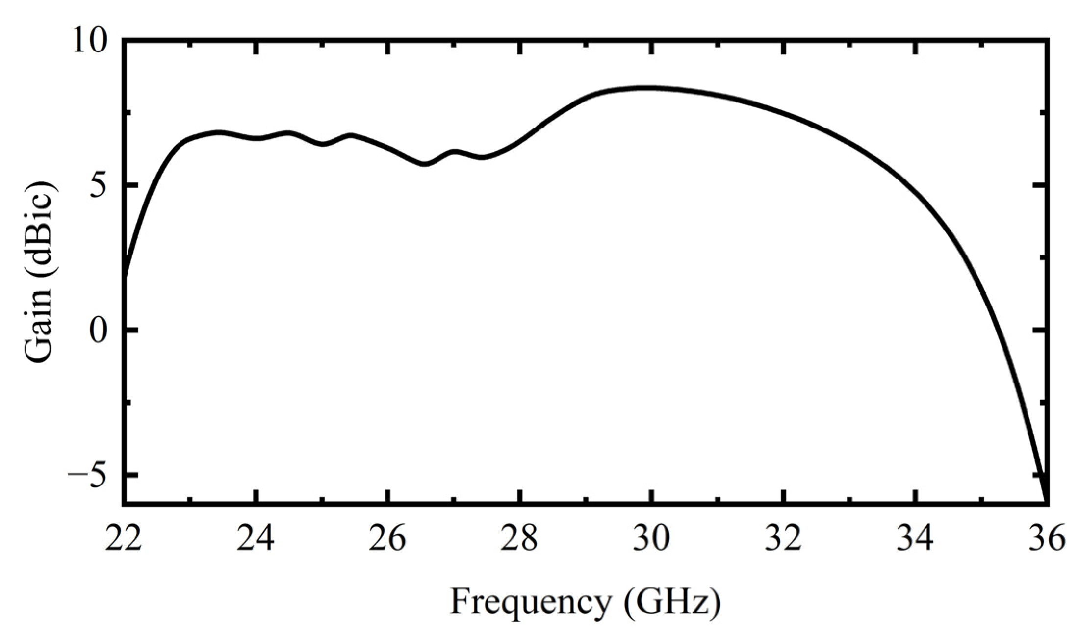
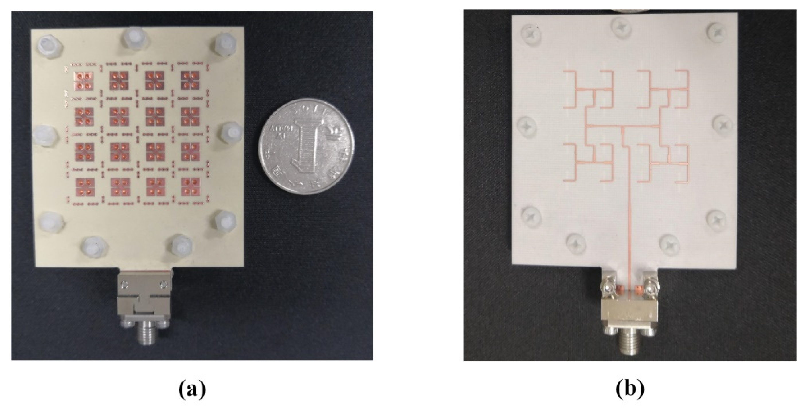
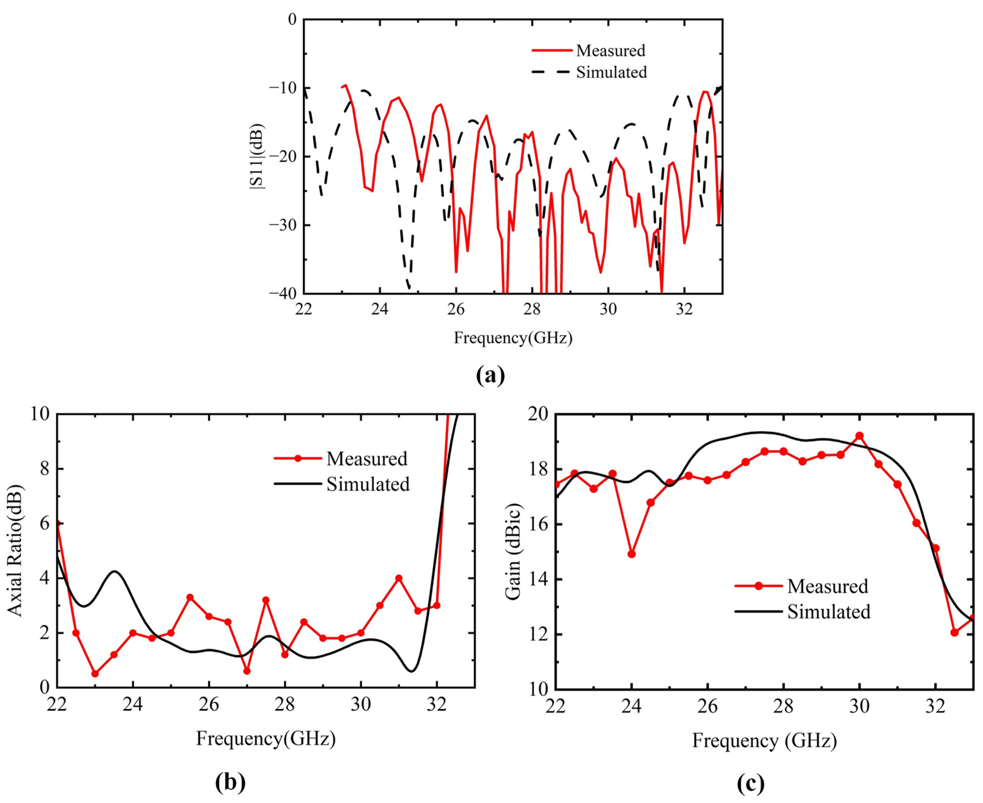
3. Results and Discussion

To validate the proposed antenna design, the 4 × 4 CP array with a power divider is fabricated based on PCB technology and experimentally tested. Figure 11 displays the photograph of the fabricated antenna array, substrate1 and substrate2 are tightly stacked by a few nylon screws. A 2.92-mm end launch connector is used to feed signals to the microstrip power divider. To ensure the accuracy of the simulation results, the simulation model includes screws and an end launch connector. Meanwhile, the assembling error is also considered in the design process and analyzed by the simulation software Ansoft HFSS.
Figure 12a,b show the S11 and AR of the antenna array. The practical test results have slight differences from the simulated ones, which is mainly attributed to the errors in fabrication and measurement. Particularly, there is some air gap between the two substrate pieces when using screws. The gap can be removed by using a bonding layer. The simulated bandwidth with S11 < −10-dB is 40%, between 22 and 33 GHz, and the measured one is more than 35.7% ranging from 23 to 33 GHz. Additionally, the simulated and measured bandwidth with AR < 3-dB is 28% (24 to 31.8 GHz) and 30.1% (22.5 to 30.5 GHz), respectively. Figure 12c depicts the broadside gains. It is seen that the experimental maximum gain is 19.2 dBic at 30 GHz, and the 3-dB gain variation spans 22 to 31 GHz, excepting the drop around 24 GHz, which may be caused by the errors in measurement.
The radiation patterns of the array at three representative frequency points are measured, as shown in Figure 13a–c. Due to the measurement limitation in our laboratory, only the results within ±40° angles are measured. The simulated and experimental data show reasonable agreement. There are some ripples in the main beam, which may be attributed to low signal-to-noise ratio in our in-house built platform [37]. The cross-polarization level is always under −10 dB at different frequencies. A high front-to-back ratio is also observed at all the frequency points.
Finally, the performances of the proposed array are compared with other Ka-band CP antenna arrays. As listed in Table 2, the overlapping impedance and AR bandwidth of the proposed design exceeds most of the referenced arrays. Although [10,18] have wider bandwidth, they need four substrate layers. Although the SIW design in [15] and the microstrip line in [26] also need two substrate layers, the bandwidth of the two arrays is much narrower. Therefore, our proposed antenna array has the advantages of broadband and fewer substrate layers.

4. Conclusions

This study presents a 4 × 4 CP ME dipole antenna array with wide bandwidth designed in the mm-wave band. To improve the bandwidth of the element, eight metallic walls are sequentially placed around the ME dipole, which work as parasitic radiators. To reduce the number of substrate layers, a compact microstrip 1-to-16 power divider is applied to excite the ME dipole array. The measured impedance bandwidth and AR bandwidth are 35.7% and 30.1%, respectively. The overlapping impedance bandwidth and AR bandwidth achieves 30.1% with a maximum gain of 19.2 dBic at 30 GHz. Due to the advantages of the planar structure, low cost, wide bandwidth, and high gain, the proposed array is very convenient to deploy on servo for beam scanning, thus it has great potential in 5G mm-wave and satellite communications.

Author Contributions

Conceptualization, B.S.; methodology, B.S.; software, B.S.; validation, B.S.; formal analysis, B.S.; investigation, B.S.; resources, C.D.; data curation, C.D.; writing—original draft preparation, C.D.; writing—review and editing, X.C.; visualization, C.D.; supervision, C.D.; project administration, C.D.; funding acquisition, C.D. All authors have read and agreed to the published version of the manuscript.

Funding

This research was funded by the National Natural Science Foundation of China under Contract 62071037.

Data Availability Statement

All data are included within manuscript.

Conflicts of Interest

The authors declare no conflict of interest.

References

  1. Azar, Y.; Wong, G.N.; Wang, K.; Mayzus, R.; Schulz, J.K.; Zhao, H.; Gutierrez, F.; Hwang, D.D.; Rappaport, T.S. 28 GHz propagation measurements for outdoor cellular communications using steerable beam antennas in New York City. In Proceedings of the 2013 IEEE International Conference on Communications (ICC), Budapest, Hungary, 9–13 June 2013; pp. 5143–5147. [Google Scholar]
  2. Zhao, Q.L.; Jin, L. Rain attenuation in millimeter wave ranges. In Proceedings of the 2006 7th International Symposium on Antennas, Propagation & EM Theory, Guilin, China, 26–29 October 2006; pp. 1–4. [Google Scholar]
  3. Deng, C.; Liu, D.; Yektakhah, B.; Sarabandi, K. Series-fed beam-steerable millimeter-wave antenna design with wide spatial coverage for 5G mobile terminals. IEEE Trans. Antennas Propag. 2019, 68, 3366–3376. [Google Scholar] [CrossRef]
  4. Gao, S.S.; Luo, Q.; Zhu, F. Introduction to Circularly Polarized Antennas; Wiley-IEEE Press: Hoboken, NJ, USA, 2014; pp. 1–28. [Google Scholar]
  5. Xu, H.; Zhou, J.; Zhou, K.; Wu, Q.; Yu, Z.; Hong, W. Planar wideband circularly polarized cavity-backed stacked patch antenna array for millimeter-wave applications. IEEE Trans. Antennas Propag. 2018, 66, 5170–5179. [Google Scholar] [CrossRef]
  6. Wu, J.; Cheng, Y.J.; Fan, Y. Millimeter-wave wideband high-efficiency circularly polarized planar array antenna. IEEE Trans. Antennas Propag. 2015, 64, 535–542. [Google Scholar] [CrossRef]
  7. Wang, Z.; Tu, Z.H. Wideband Circularly Polarized Antenna Array Using three-layer Segmented Patches for Q-band Application. IEEE Antennas Wirel. Propag. Lett. 2022. [Google Scholar] [CrossRef]
  8. Ji, Z.; Sun, G.H.; Wong, H. A Wideband Circularly Polarized Complementary Antenna for Millimeter-Wave Applications. IEEE Trans. Antennas Propag. 2022, 70, 2392–2400. [Google Scholar] [CrossRef]
  9. Gan, Z.; Tu, Z.H.; Xie, Z.M.; Chu, Q.X.; Yao, Y. Compact wideband circularly polarized microstrip antenna array for 45 GHz application. IEEE Trans. Antennas Propag. 2018, 66, 6388–6392. [Google Scholar] [CrossRef]
  10. Wu, Q.; Hirokawa, J.; Yin, J.; Yu, C.; Wang, H.; Hong, W. Millimeter-wave planar broadband circularly polarized antenna array using stacked curl elements. IEEE Trans. Antennas Propag. 2017, 65, 7052–7062. [Google Scholar] [CrossRef]
  11. Zhang, L.; Wu, K.; Wong, S.W.; He, Y.; Chu, P.; Li, W.; Gao, S. Wideband high-efficiency circularly polarized SIW-fed S-dipole array for millimeter-wave applications. IEEE Trans. Antennas Propag. 2019, 68, 2422–2427. [Google Scholar] [CrossRef]
  12. Sadeghi-Marasht, S.; Sharawi, M.S.; Zhu, A. Dual-Band Circularly Polarized Antenna Array for 5G Millimeter-Wave Applications. IEEE Open J. Antennas Propag. 2022, 3, 314–323. [Google Scholar] [CrossRef]
  13. Zhu, Q.; Ng, K.B.; Chan, C.H. Printed circularly polarized spiral antenna array for millimeter-wave applications. IEEE Trans. Antennas Propag. 2016, 65, 636–643. [Google Scholar] [CrossRef]
  14. Liu, C.; Guo, Y.X.; Bao, X.; Xiao, S.Q. 60-GHz LTCC integrated circularly polarized helical antenna array. IEEE Trans. Antennas Propag. 2012, 60, 1329–1335. [Google Scholar] [CrossRef]
  15. Han, W.; Yang, F.; Ouyang, J.; Yang, P. Low-cost wideband and high-gain slotted cavity antenna using high-order modes for millimeter-wave application. IEEE Trans. Antennas Propag. 2015, 63, 4624–4631. [Google Scholar] [CrossRef]
  16. Wang, X.C.; Xia, Y.J.; Yang, J.H.; Lu, W.Z. Wideband High-Gain Circularly Polarized Substrate Integrated Cavity Antenna Array for Millimeter-Wave Applications. IEEE Trans. Antennas Propag. 2022, 71, 1041–1046. [Google Scholar] [CrossRef]
  17. Li, Y.; Chen, Z.N.; Qing, X.; Zhang, Z.; Xu, J.; Feng, Z. Axial ratio bandwidth enhancement of 60-GHz substrate integrated waveguide-fed circularly polarized LTCC antenna array. IEEE Trans. Antennas Propag. 2012, 60, 4619–4626. [Google Scholar] [CrossRef]
  18. Wen, L.; Gao, S.; Hu, W.; Luo, Q.; Yang, X.X.; Sanz-Izquierdo, B. Wideband Differentially-Fed Slot Antenna and Array with Circularly Polarized Radiation for Millimeter-Wave Applications. IEEE Trans. Antennas Propag. 2022, 70, 5418–5429. [Google Scholar] [CrossRef]
  19. Yang, M.D.; Pan, Y.M.; Sun, Y.X.; Leung, K.W. Wideband circularly polarized substrate-integrated embedded dielectric resonator antenna for millimeter-wave applications. IEEE Trans. Antennas Propag. 2019, 68, 1145–1150. [Google Scholar] [CrossRef]
  20. Yang, W.W.; Sun, W.J.; Tang, H.; Chen, J.X. Design of a circularly polarized dielectric resonator antenna with wide bandwidth and low axial ratio values. IEEE Trans. Antennas Propag. 2019, 67, 1963–1968. [Google Scholar] [CrossRef]
  21. Attia, H.; Abdalrazik, A.; Sharawi, M.S.; Kishk, A.A. Wideband Circularly-Polarized Millimeter-Wave DRA Array for Internet of Things. IEEE Internet Things J. 2023. [Google Scholar] [CrossRef]
  22. Feng, B.; Lai, J.; Chung, K.L.; Chen, T.Y.; Liu, Y. A compact wideband circularly polarized magneto-electric dipole antenna array for 5G millimeter-wave application. IEEE Trans. Antennas Propag. 2020, 68, 6838–6843. [Google Scholar] [CrossRef]
  23. Wu, J.; Huang, Z.; Ren, X.; Wei, E.I.; Wu, X. Wideband millimeter-wave dual-mode dual circularly polarized OAM antenna using sequentially rotated feeding technique. IEEE Antennas Wirel. Propag. Lett. 2020, 19, 1296–1300. [Google Scholar] [CrossRef]
  24. Guan, D.F.; Ding, C.; Qian, Z.P.; Zhang, Y.S.; Guo, Y.J.; Gong, K. Broadband high-gain SIW cavity-backed circular-polarized array antenna. IEEE Trans. Antennas Propag. 2016, 64, 1493–1497. [Google Scholar] [CrossRef]
  25. Lai, H.W.; Xue, D.; Wong, H.; So, K.K.; Zhang, X.Y. Broadband circularly polarized patch antenna arrays with multiple-layers structure. IEEE Antennas Wirel. Propag. Lett. 2016, 16, 525–528. [Google Scholar] [CrossRef]
  26. Xu, J.; Hong, W.; Jiang, Z.H.; Zhang, H.; Wu, K. Low-profile wideband vertically folded slotted circular patch array for Ka-band applications. IEEE Trans. Antennas Propag. 2020, 68, 6844–6849. [Google Scholar] [CrossRef]
  27. Baghernia, E.; Movahedinia, R.; Sebak, A.R. Broadband compact circularly polarized spiral antenna array fed by printed gap waveguide for millimeter-wave applications. IEEE Access 2020, 9, 86–95. [Google Scholar] [CrossRef]
  28. Jiang, Z.H.; Wu, F.; Yue, T.; Hong, W. Wideband and low-profile integrated dual-circularly-polarized transmit-arrays enabled by antenna-filter-antenna phase shifting cells. IEEE Trans. Antennas Propag. 2021, 69, 7462–7475. [Google Scholar] [CrossRef]
  29. Yang, Y.H.; Zhou, S.G.; Sun, B.H.; Gao, X.Z. Design of wideband circularly polarized antenna array excited by substrate integrated coaxial line for millimeter-wave applications. IEEE Trans. Antennas Propag. 2021, 69, 8943–8948. [Google Scholar] [CrossRef]
  30. Pan, Y.M.; Yang, W.J.; Zheng, S.Y.; Hu, P.F. Design of wideband circularly polarized antenna using coupled rotated vertical metallic plates. IEEE Trans. Antennas Propag. 2017, 66, 42–49. [Google Scholar] [CrossRef]
  31. Yang, M.; Pan, Y.; Yang, W. A singly fed wideband circularly polarized dielectric resonator antenna. IEEE Antennas Wirel. Propag. Lett. 2018, 17, 1515–1518. [Google Scholar] [CrossRef]
  32. Yang, W.J.; Pan, Y.M.; Zheng, S.Y. A low-profile wideband circularly polarized crossed-dipole antenna with wide axial-ratio and gain beamwidths. IEEE Trans. Antennas Propag. 2018, 66, 3346–3353. [Google Scholar] [CrossRef]
  33. Qi, Z.; Zhu, Y.; Li, X. Compact wideband circularly polarized patch antenna array using self-sequential rotation technology. IEEE Antennas Wirel. Propag. Lett. 2022, 21, 700–704. [Google Scholar] [CrossRef]
  34. Cheng, Y.; Dong, Y. Wideband circularly polarized planar antenna array for 5G millimeter-wave applications. IEEE Trans. Antennas Propag. 2020, 69, 2615–2627. [Google Scholar] [CrossRef]
  35. Zhu, J.; Liao, S.; Li, S.; Xue, Q. 60 GHz wideband high-gain circularly polarized antenna array with substrate integrated cavity excitation. IEEE Antennas Wirel. Propag. Lett. 2018, 17, 751–755. [Google Scholar] [CrossRef]
  36. Li, Y.; Luk, K.M. A 60-GHz wideband circularly polarized aperture-coupled magneto-electric dipole antenna array. IEEE Trans. Antennas Propag. 2016, 64, 1325–1333. [Google Scholar] [CrossRef]
  37. Cano, F.J.; Burgos, S.; Sierra, M. Novel method to improve the signal-to-noise ratio in far-field results obtained from planar near-field measurements. IEEE Antennas Propag. Mag. 2011, 53, 215–220. [Google Scholar] [CrossRef]
Figure 1. Geometry of the CP element: (a) 3D explosive view; (b) top layer; (c) bottom layer.
Electronics 12 02154 g001
Figure 2. Evolution process of the proposed CP element.
Electronics 12 02154 g002
Figure 3. Simulated performance of the different types of CP antennas: (a) simulated S11 of the antennas; (b) simulated AR of the antennas.
Electronics 12 02154 g003
Figure 4. Currents on the ME dipole and vertical metallic walls: (a) 26 GHz, t = 0°; (b) 26 GHz, t = 90°; (c) 32 GHz, t = 0°; (d) 32 GHz, t = 90°.
Electronics 12 02154 g004
Figure 5. Simulated AR for three parameters of the ME dipole: (a) width of the metalized strip used to connect the diagonally located patches P; (b) interval between adjacent patches G; (c) interval between the metalized strip and patch G3.
Electronics 12 02154 g005
Figure 6. Simulated AR for different parameters of vertical metallic walls: (a) spacing between the metal walls and the patches along the x-axis direction D1; (b) spacing between the metal walls and the patches along the y-axis direction D2; (c) spacing between the metal walls along the x-axis direction D3; (d) spacing between the metal walls along the y-axis direction D4; (e) lengths of the metal walls along the x-axis direction L3; (f) lengths of the metal walls along the y-axis direction L4.
Electronics 12 02154 g006
Figure 7. Simulated gain of the CP element.
Electronics 12 02154 g007
Figure 8. Simulated normalized radiation patterns of the CP element at three separate frequency points: (a) 24 GHz; (b) 28 GHz; (c) 32 GHz.
Electronics 12 02154 g008
Figure 9. Configuration of the 4 × 4 array prototype: (a) top-down view; (b) bottom-up view.
Electronics 12 02154 g009
Figure 10. Geometry and simulated S-parameters results of the T-junction: (a) geometry; (b) simulated S parameters results.
Electronics 12 02154 g010
Figure 11. Photograph of the fabricated array: (a) top-down view; (b) bottom-up view.
Electronics 12 02154 g011
Figure 12. Simulated and measured results of the antenna array: (a) S11; (b) AR; (c) gain.
Electronics 12 02154 g012
Figure 13. Simulated and measured radiation normalized patterns of the proposed antenna array: (a) 24 GHz; (b) 28 GHz; (c) 31 GHz.
Electronics 12 02154 g013
Table 1. Specified dimensions for the proposed CP element (unit: mm).
ParameterValueParameterValueParameterValue
L12.06G30.11S21.9
L22D11.8P0.93
L32.9D21.9Wf0.22
L41.3D30.7Df0.49
G10.32D44.1Ws0.36
G20.32S12.35Ls3
Table 2. Comparison between planar MM-wave CP arrays with different feeding structures.
Ref.Center
Frequency (GHz)
No. of Substrate LayersNo. of ElementsFeeding
Network
Impedance
BW (%)
AR
BW (%)
Peak Gain
(dBic)
Size
0 × λ0 × λ0)
[5]2924 × 4CPW + SIW29.625.420.3210.2 × 8.7 × 0.098
[6]28.3544 × 4Microstrip line28.61418.26.72 × 4.48 × 0.2
[10]37.548 × 8SIW35.433.823.56 × 6 × 0.339
[11]3038 × 8SIW27.632.725.26.1 × 6.1 × 0.47
[15]33.524 × 4SIW14.91113.21.76 × 1.76 × 0.32
[18]27.444 × 4Microstrip line + dual feed39.433.618.54.58 × 4.31 × 0.16
[22]2734 × 4CPW27.727.820.27 × 5 × 0.42
[26]29.2524 × 4Microstrip line58.4613.6814.695.2 × 5.2 × 0.08
This Work2824 × 4Microstrip line35.730.119.24.92 × 5.57 × 0.14
Disclaimer/Publisher’s Note: The statements, opinions and data contained in all publications are solely those of the individual author(s) and contributor(s) and not of MDPI and/or the editor(s). MDPI and/or the editor(s) disclaim responsibility for any injury to people or property resulting from any ideas, methods, instructions or products referred to in the content.

