Article

Programmable Beam-Steering Capabilities Based on Graphene Plasmonic THz MIMO Antenna via Reconfigurable Intelligent Surfaces (RIS) for IoT Applications

by
Sherif A. Khaleel
1,2,*,
Ehab K. I. Hamad
2,*,
Naser Ojaroudi Parchin
3,* and
Mohamed B. Saleh
1
1
College of Engineering and Technology, Arab Academy for Science, Technology and Maritime Transport, Aswan 81511, Egypt
2
Electrical Engineering Department, Faculty of Engineering, Aswan University, Aswan 81542, Egypt
3
School of Engineering and the Built Environment, Edinburgh Napier University, Edinburgh EH10 5DT, UK
*
Authors to whom correspondence should be addressed.
Electronics 2023, 12(1), 164; https://doi.org/10.3390/electronics12010164
Submission received: 15 November 2022 / Revised: 23 December 2022 / Accepted: 27 December 2022 / Published: 29 December 2022
(This article belongs to the Special Issue Antenna Designs for 5G/IoT and Space Applications, Volume II)

Abstract

:
The approaching sixth-generation (6G) communication network will modernize applications and satisfy user demands through implementing a smart and reconfigurable system with a higher data rate and wider bandwidth. The controllable THz waves are highly recommended for the instantaneous development the new technology in wireless communication systems. Recently, reconfigurable intelligent surfaces (RIS), also called codded/tunable programmable metasurfaces, have enabled a conspicuous functionality for THz devices and components for influencing electromagnetic waves (EM) such as beam steering, multi-beam-scanning applications, polarization variation, and beam focusing applications. In this article, we proposed a graphene plasmonic two-port MIMO microstrip patch antenna structure that operates at a 1.9 THz resonance frequency. An E-shape MTM unit cell is introduced to enhance the isolation of the antenna from −35 dB to −54 dB. An implementation of controllable and reconfigurable surfaces based on graphene meta-atoms (G-RIS) placed above the radiating patches with a suitable separated distance to control the radiated beam to steer in different directions (±60°). The reconfigurable process is carried out via changing the (ON/OFF) meta-atoms states to get a specific code with a certain beam direction. The gain enhancement of the antenna can be implemented through an artificial magnetic conductor (AMC) based on graphene material. The G-AMC layer is located underneath the (MIMO antenna, G-RIS layer) to improve the gain from 4.5 dBi to 10 dBi. The suggested antenna structure results are validated with different techniques CST microwave studio and ADS equivalent circuit model. The results have asymptotic values. So, the proposed design of the MIMO antenna that is sandwiched between G-RIS and G-AMC is suitable for IoT applications.

1. Introduction

The presently used frequency spectrum (e.g., microwave, millimeter wave) is insufficient to meet the demands of wireless communication due to the exponential development of data traffic in sixth-generation (6G) applications. The terahertz frequency spectrum is ranging from 0.1 THz to 10 THz, which provides large bandwidth and achieves an extremely high-speed data rate of up to several terabit per second (Tbps). So, it has attracted great attention all over the world. Recently, the THz spectrum opened the door for researchers from both industry and academicians to use it in numerous applications such as wireless communications, biomedical applications, imaging, spectroscopy, and aerospace applications [1,2,3]. The THz wireless communications are preferable for short-distance indoor applications due to the free space path loss, which is relevant at THz frequencies compared to mm-Wave. The THz band offers a lot of potential for future 6th-generation wireless communication technologies. In a wireless medium, EM waves are attenuated by material absorption loss and wave dispersion owing to reflection, refraction, and diffraction, leading to many propagation pathways between devices. So, the system gets uncontrollable due to the multipath fading problem. By the way, introducing metasurfaces (Artificial magnetic conductor structures) layer is a good candidate to overcome these limitations. The metasurface is a type of MTM with an artificial unit cell structure that repeated in a periodic manner. Due to their versatile qualities and properties, metasurfaces have found widespread use in recent years. It also has a wide range of applications such as perfect absorption applications [3], wireless power transfer [4], wave fronts with reflectionless sheets [5], polarization controllability [6], beam splitting and forming [7,8], total reflection or transmission layers [9,10], and its gained the researcher attentions in the wireless communications because of the total controllability and tunability of the wave propagations and its directions [11]. This tunability means that all the meta-atoms (unit cells) are controlled by switching it from ON to OFF state (modulated) by changing the external biasing gate voltage. This tunability or in another word reconfigurability can be realized electrically, optically, thermally, mechanically, or chemically. This property can change the response of the meta-atoms from the absorption mode to the reflection or transmission mode of operations by controlling the biasing voltage [12]. The tunable Metasurfaces or the reconfigurable capability of the meta-atoms is named in many research papers as a reconfigurable intelligent surface (RIS) or intelligent reflecting surfaces (IRS). Additionally, it could be considered as a special kind of the artificial magnetic conductors (AMC). The RIS is a good candidate in the new revolution of the 6G wireless communications systems and the Terahertz (THz) frequency band applications.
The conventional metasurfaces in the microwave band are implemented using copper material as a conducting element to make the tunability and reconfigurability process. In the THz band, the copper material is lake the reconfigurability and the adaptability property. Additionally, copper material is not stable in the THz band and its behavior may be changed in this band. The electrical conductivity of copper is excellent in the radio frequency (RF) and microwave (MW) ranges, but it degrades in the terahertz (THz) region. Lower THz frequency ranges cause a reduction in copper’s skin depth and conductivity. As a result, the ohmic resistance contributes more to the copper’s surface impedance than anything else. This presents a considerable difficulty for antenna design in the THz frequency range. Copper’s low conductivity and shallow skin cause significant propagation losses in the terahertz frequency range, reducing the material’s overall radiation efficiency [13]. So, the graphene material has great potential for the design of meta-atoms because of its tunable and reconfigurable properties. Graphene is a prominent material that gives the opportunity in making reconfigurable devices, especially in the THz band [14,15]. Graphene is a single-layer material with remarkable capabilities in a wide range of areas, including electricity, mechanics, heat, and light. Supporting the propagation of surface plasmon polariton (SPP) waves in the THz frequency band is the most significant property of graphene. Graphene’s conductivity and chemical potential are both dynamically influenced by an external electric field applied through a gate voltage [16]. The reconfigurability or tunability of the graphene material pushes the researchers to go forward in the usage of the graphene material as a RIS in THz communications [17]. Recently, reconfigurable antennas have attracted the researchers’ attention in 6G wireless communications. The beam scanning or beam forming types are widely studied in the last few years, due to their critical role in phased array systems. The reconfigurable property of the antenna can be implemented by different techniques of electrical or mechanical switches such as p-i-n diodes, varactor diodes, and micro-electromechanical system switches (MEMS) [14,18]. Unfortunately, these types of switches cannot be used in the microscale of the THz spectrum. So, the graphene-based antenna structures reveal many advantages for tunable THz devices due to the tunable graphene conductivity.
The MIMO antenna structure is a good candidate for the usage of the graphene based RIS for THz applications. The isolation between the MIMO antenna patches is considered the harmful parameter that reduces the antenna’s efficiency. So, introducing the graphene material as a conducting element in the MIMO structure has a good impact on reducing the mutual coupling problem. This impact is due to the short SPP wavelength of the graphene due to the SPP wave’s sluggish transmission. As a result, the graphene- MIMO antenna structure gives a fewer mutual coupling effect than the metallic one at the same preparation conditions. The MTM structure is a good way used to reduce the mutual coupling. It’s considered a band-stop filter between the radiating elements. The existence of the MTM reduces mutual coupling, which in turn increases diversity gain (DG), decreases channel capacity loss (CCL), and improves antenna efficiency.
Herein the article is organized as follows and depicted in the flowchart in Figure 1. The following Section 2 depicts the material properties of graphene that are important from the MIMO antenna and RIS point of view. Section 3 is summarized as follows; it is start by designing single and two-port MIMO graphene-based antennas and reducing their mutual coupling via E-shape MTM. It also discusses placing a G-RIS superstrate layer above the MIMO antenna to reconfigure the gain and produce beam steering in different directions. There also a G-AMC layer is introduced to increase the gain of the antenna. Finally, the last Section 4 introduced the paper’s conclusion. The novelty in this paper can be summarized as follows:
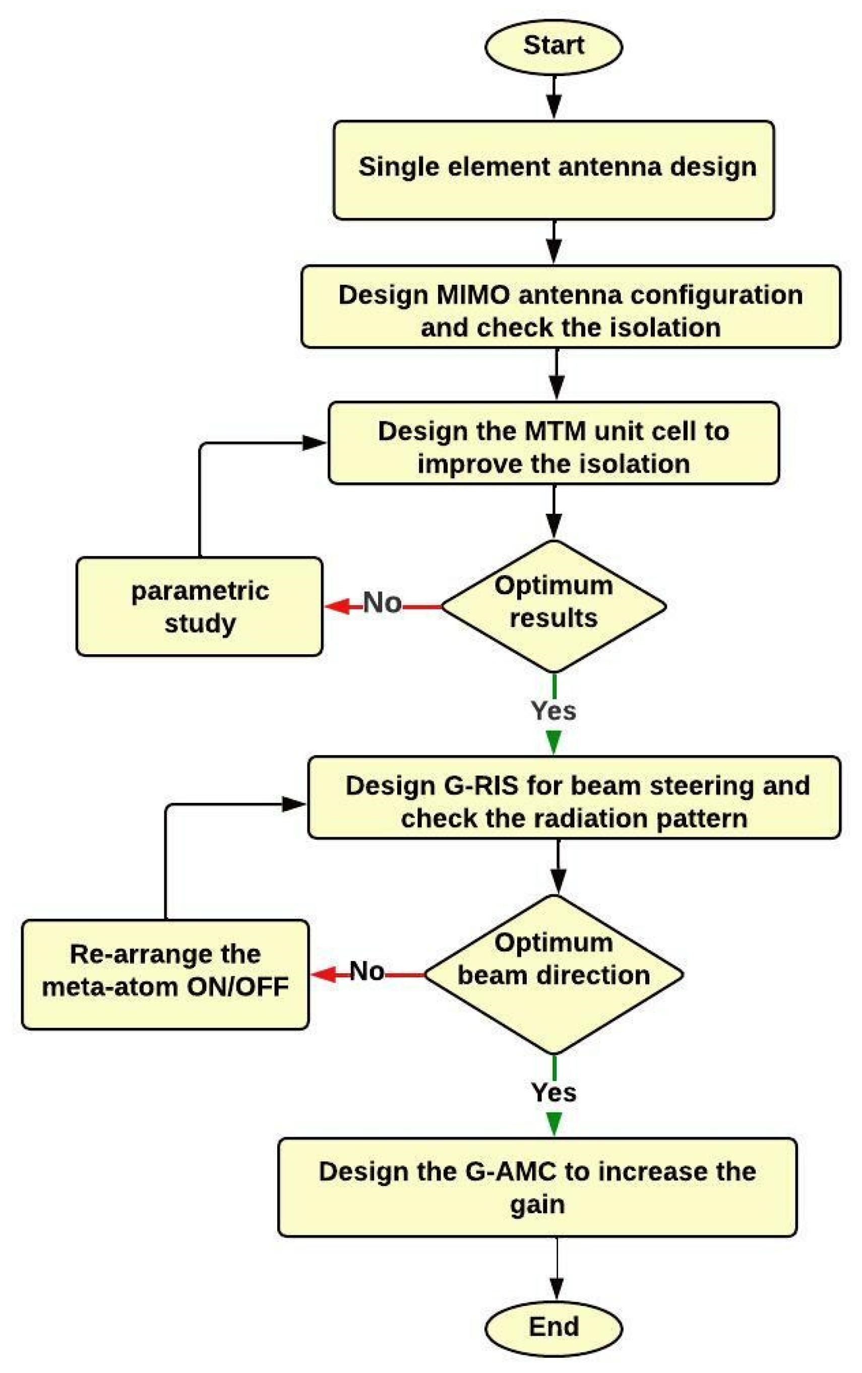
  • Design a graphene plasmonic MIMO antenna to be operated at 1.9 THz.
  • Introduced the E-shaped MTM structure between the MIMO element to increase the isolation between the elements and enhance the MIMO antenna performance.
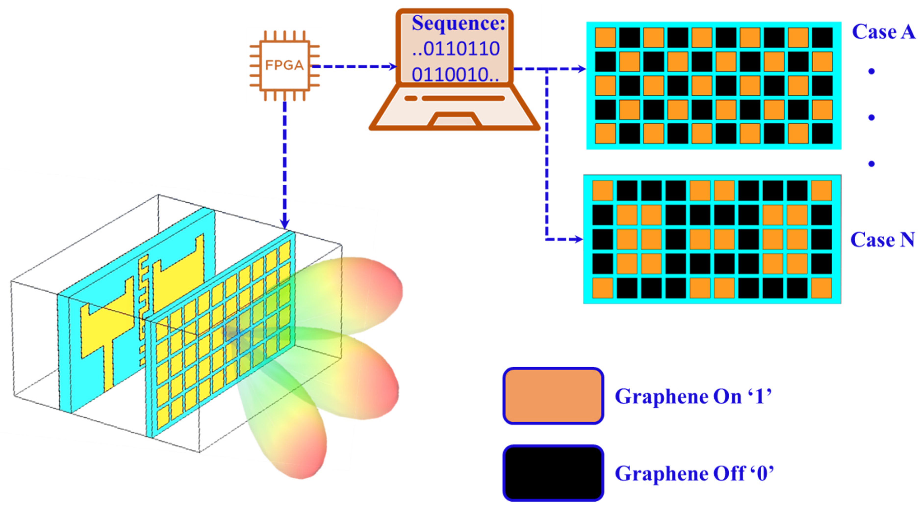
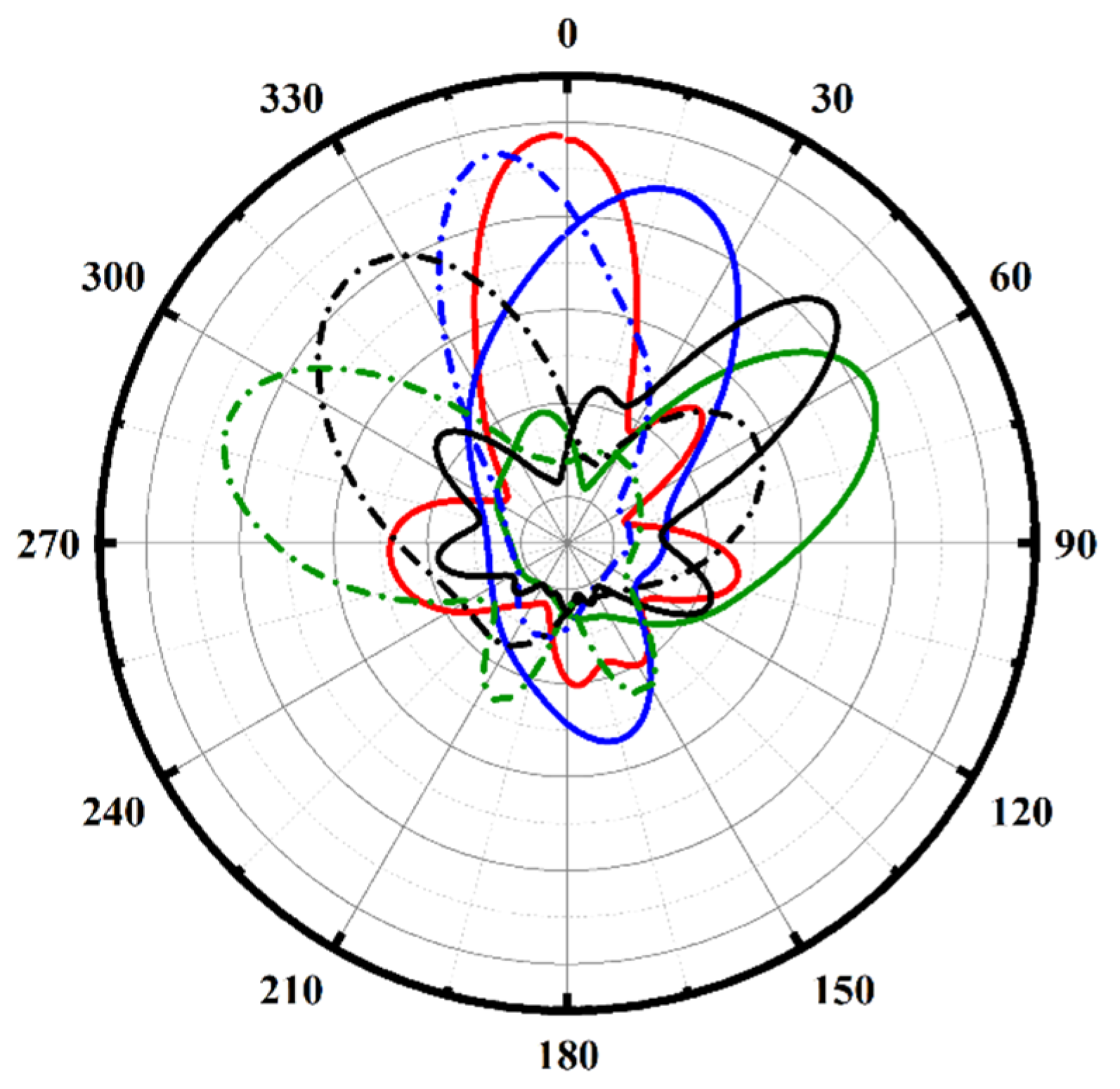
  • The graphene reconfigurable intelligent surfaces (G-RIS) used as a superstrate layer to control the beam direction from +60° to −60°. The beam-steering capability is used in indoor THz applications, so this antenna is a good candidate for these applications.
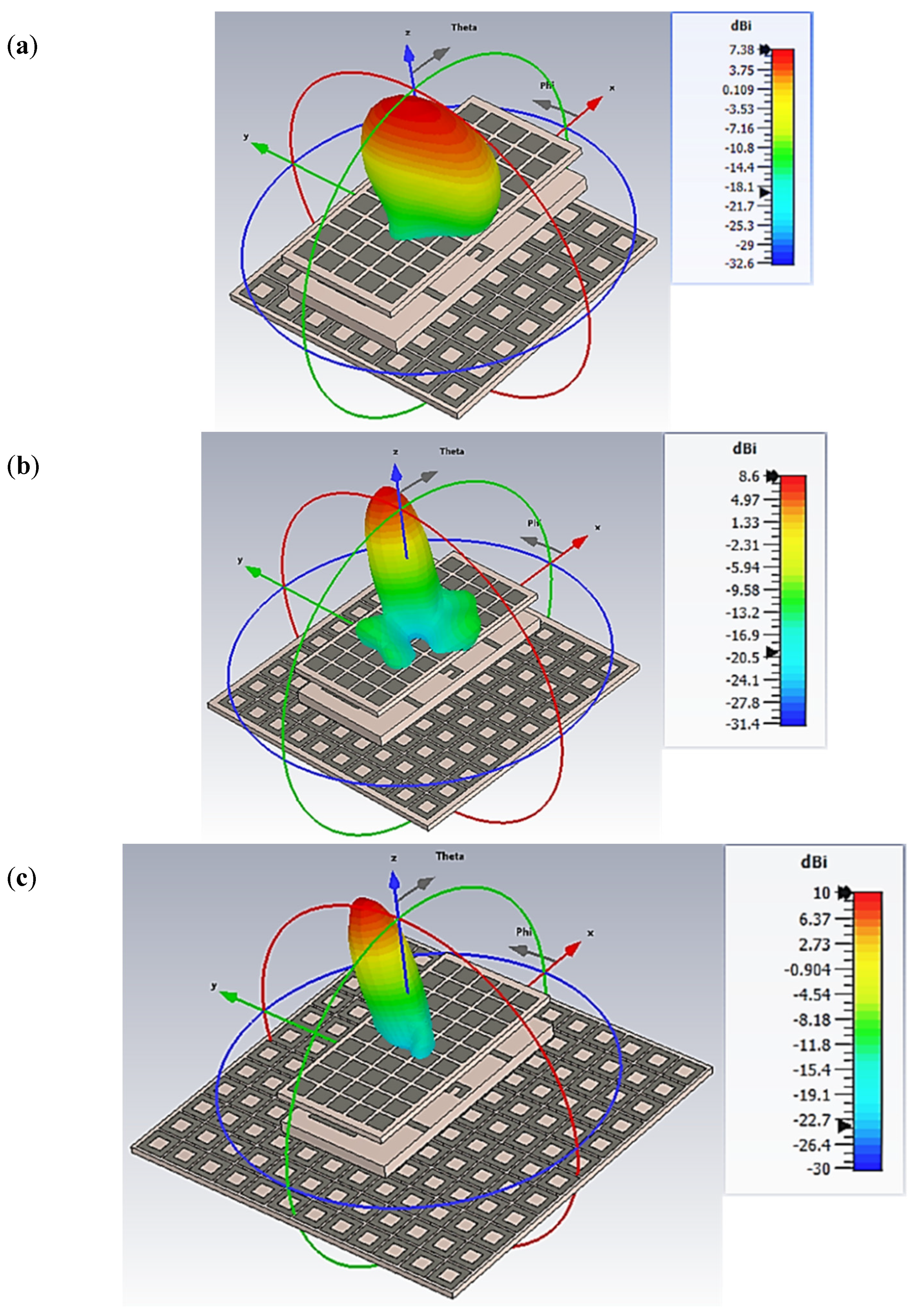
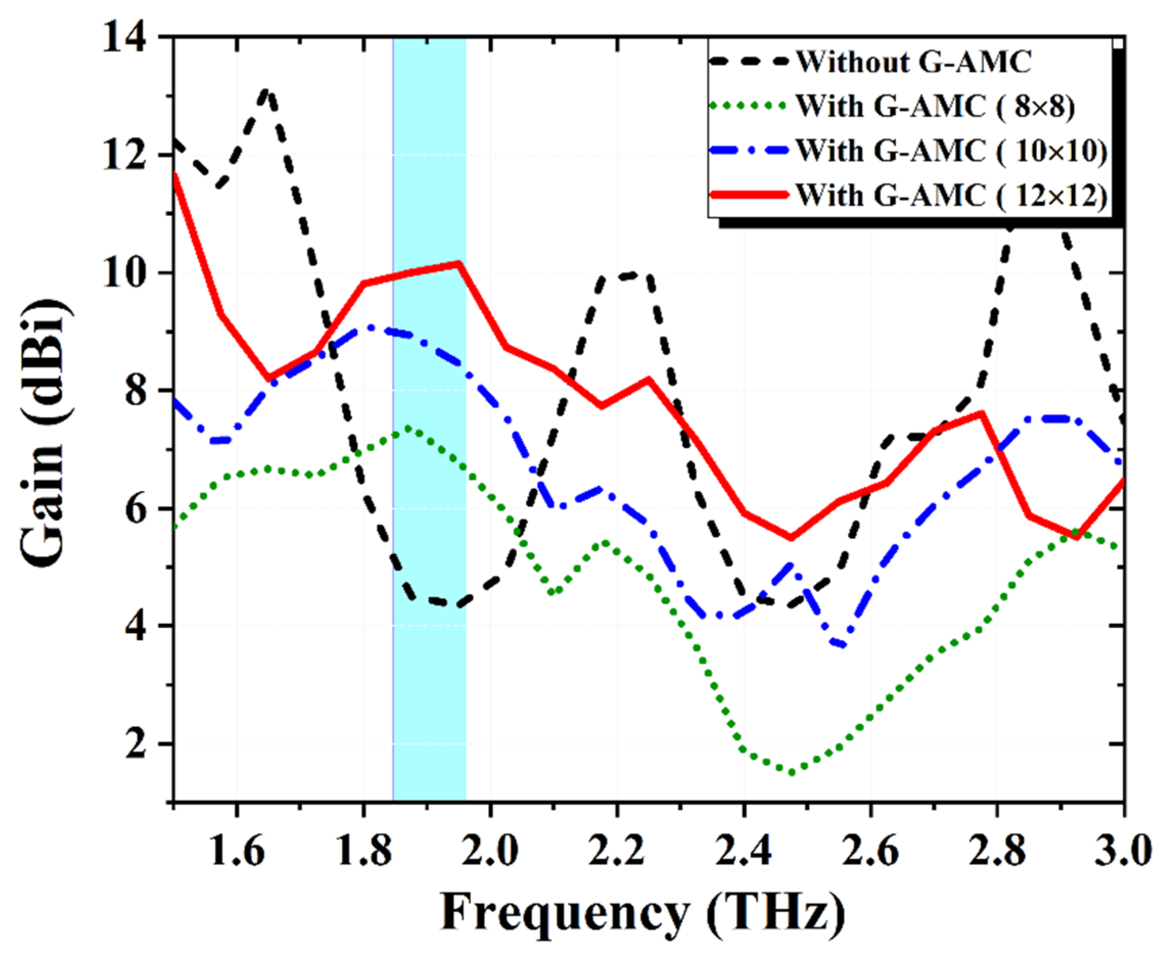
  • As the gain of the proposed design of the MIMO antenna + GRIS layer is small, so an artificial magnetic conductor layer from the graphene material (G-AMC) is introduced. This layer is used beneath the antenna structure at a certain height.

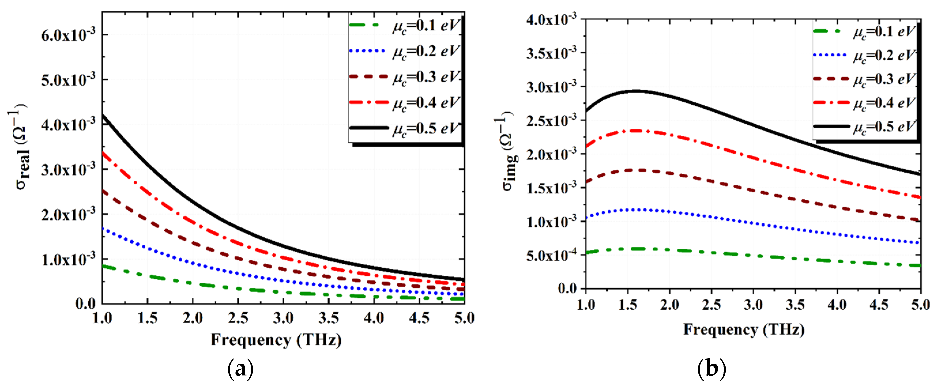
2. Graphene Material Properties

The graphene nanomaterial is a two- dimensional infinitesimal thin monolayer of carbon atoms arranged in a highly ordered manner in a hexagonal lattice unit cell. The extraordinary properties of the graphene material especially in the THz frequency band open plenty of applications in several fields [19]. The plasmonic wave propagation in the THz band depends on the graphene material with low losses and good tunability. The conductivity of graphene is characterized using the Drude model [20]. It is consisting of two main terms due to the interband and intraband contributions and it is given by:
σ s ( ω , μ c , τ , T ) = σ i n t e r + j σ i n t r a      
σ s , i n t e r ( ω , μ c , τ , T ) = j e 2 4 π l n [ 2 | μ c | ( ω j τ 1 ) 2 | μ c | + ( ω j τ 1 ) ]
σ s , i n t r a ( ω , μ c , τ , T ) = j e 2 K B T π 2 ( ω j τ 1 ) [ μ c K B T + 2 ln ( e μ c / K B T + 1 ) ]
where ω is the angular frequency, μ c is the chemical potential, τ is the relaxation time, T is the temperature, K B is Boltzmann’s constant, and is the reduced Planck’s constant. The graphene conductivity is controlled by adjusting the chemical potential which depends on the free carrier density. It can be changed by varying the gate voltage, electric field, magnetic field, and/or chemical doping. The chemical potential, given in terms of the biasing voltage V g looks similar to that in [21,22]:
μ c = υ f π C o x V g e ,   and   C o x = ε o ε r t  
where C o x is the gate capacitance, ε r is the relative permittivity, ε o free space permittivity, υ f is the Fermi velocity of Dirac fermions in graphene υ f = 10 6   m / s , and t is the height of the substrate. The graphene permittivity can be obtained by its conductivity [23].
ε g = 1 + j σ s t g ε o ω  
where t g is the thickness of graphene layer. From the presented equations we can conclude that Graphene’s characteristics, including its conductivity and permittivity, are dynamically influenced by an applied gate voltage. This property enables the reconfigurability process of graphene-based devices. Figure 2 shows the variations of the graphene surface conductivity with frequency for different chemical potential values and τ = 1   ps at T = 300 K.

3. Antenna Design

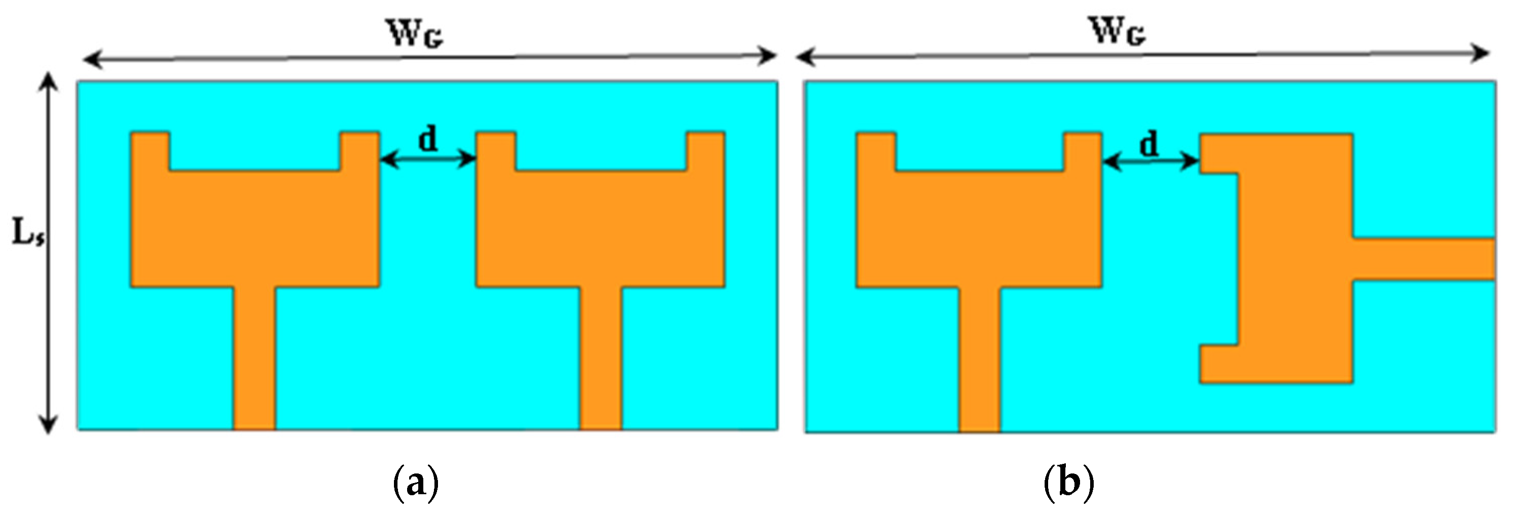
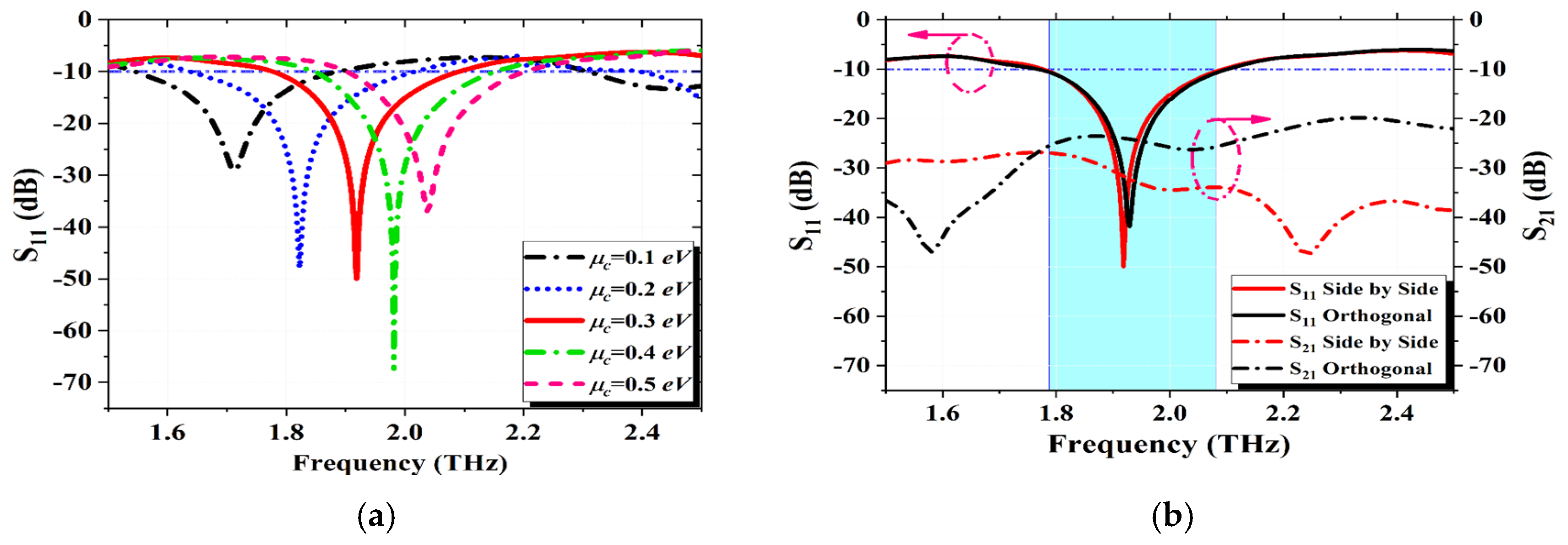
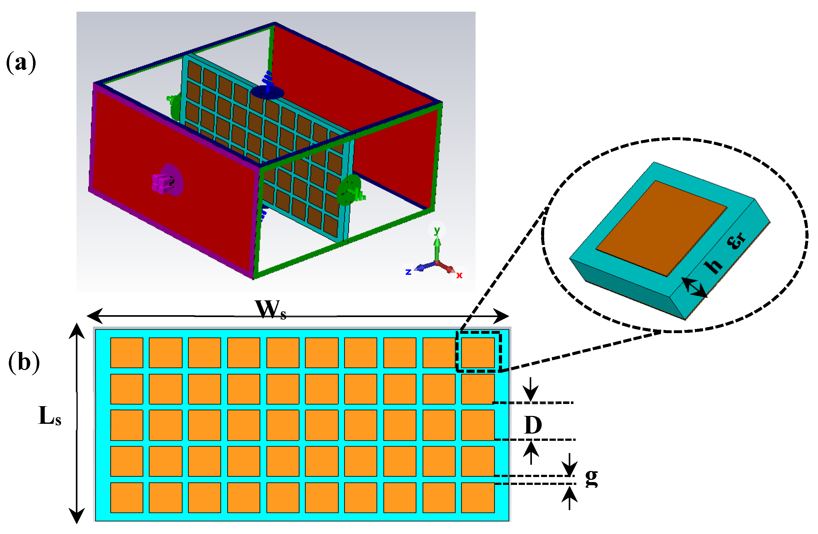
3.1. Graphene MIMO Antenna Configurations

In recent years, MIMO configuration systems have received a lot of attention due to their usefulness in boosting data rates despite the existence of signal fading, multipath fading, and interference. To transmit more data over a farther distance while maintaining acceptable MIMO characteristics, a MIMO system is developed. In MIMO antennas, mutual coupling is the key issue that needs to be considered. Therefore, it is desirable to minimize it as much as possible to improve system performance. Figure 2 demonstrated the proposed two configurations of the MIMO elements. The first one is side-by-side, while the other configuration is the orthogonal one as shown in Figure 3a,b. The antenna is designed using a polyamide substrate with a thickness and dielectric constant of 10 µm and 3.5, respectively. Also, the proposed antenna parameters are listed in Table 1. The graphene material is used as the conducting layer. Surface plasmon polariton (SPP) waves propagate more easily via graphene material compared to other plasmonic materials such as gold or silver. The CST microwave studio suite (2021) is used to analyze the performance of the proposed graphene MIMO antenna. It is considered the most powerful multilayer 3D full-wave electromagnetic solver, which accurately solves the Maxwell equations using the Finite Element Method (FEM) technique. For modelling graphene, the CST software includes both a graphene and a graphene-Eps model. The graphene model expressed in the CST with a thickness of 0.345 nm is considered a single layer of graphene, while the graphene-EPS is expressed as a multilayer of graphene sheets with a suitable thickness. In our proposed antenna design, we introduced the graphene model with a different chemical potential value from 0.1 eV to 0.5 eV and relaxation time of 0.1 psec, and a room temperature of 300 K. Figure 4a shows how changing the chemical potentials affects the frequency response of the graphene plasmonic antenna. This figure reveals that the antenna resonance frequency increases by increasing the chemical potential value. So, the design of the proposed is dynamically controlled and reconfigurable, which is a plethora of THz antenna technology. Figure 4b illustrates the S11 and S21 of the graphene MIMO antenna configurations, which resonate at 1.9 THz. The reflection coefficient S11 of the two configurations is almost the same, while the isolation coefficient S21 between antenna elements is better in the case of the side-by-side orientation than the orthogonal one. The S21 of the orthogonal one is reached −25 dB in the desired bandwidth, while this value is reached −35dB in the side-by-side configuration. So, side-by-side orientation is suggested in the MIMO antenna design.

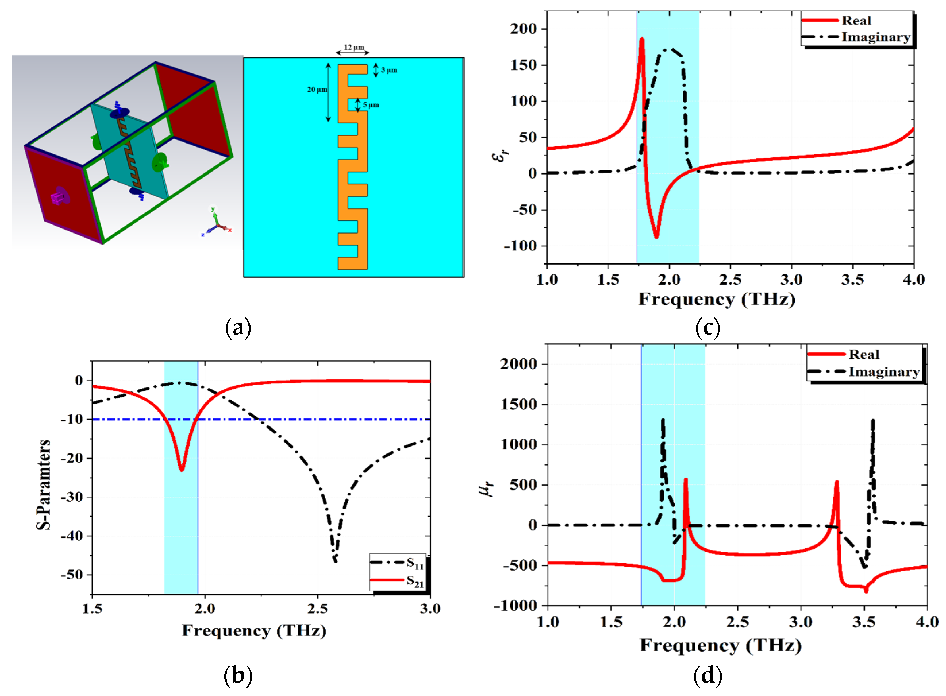
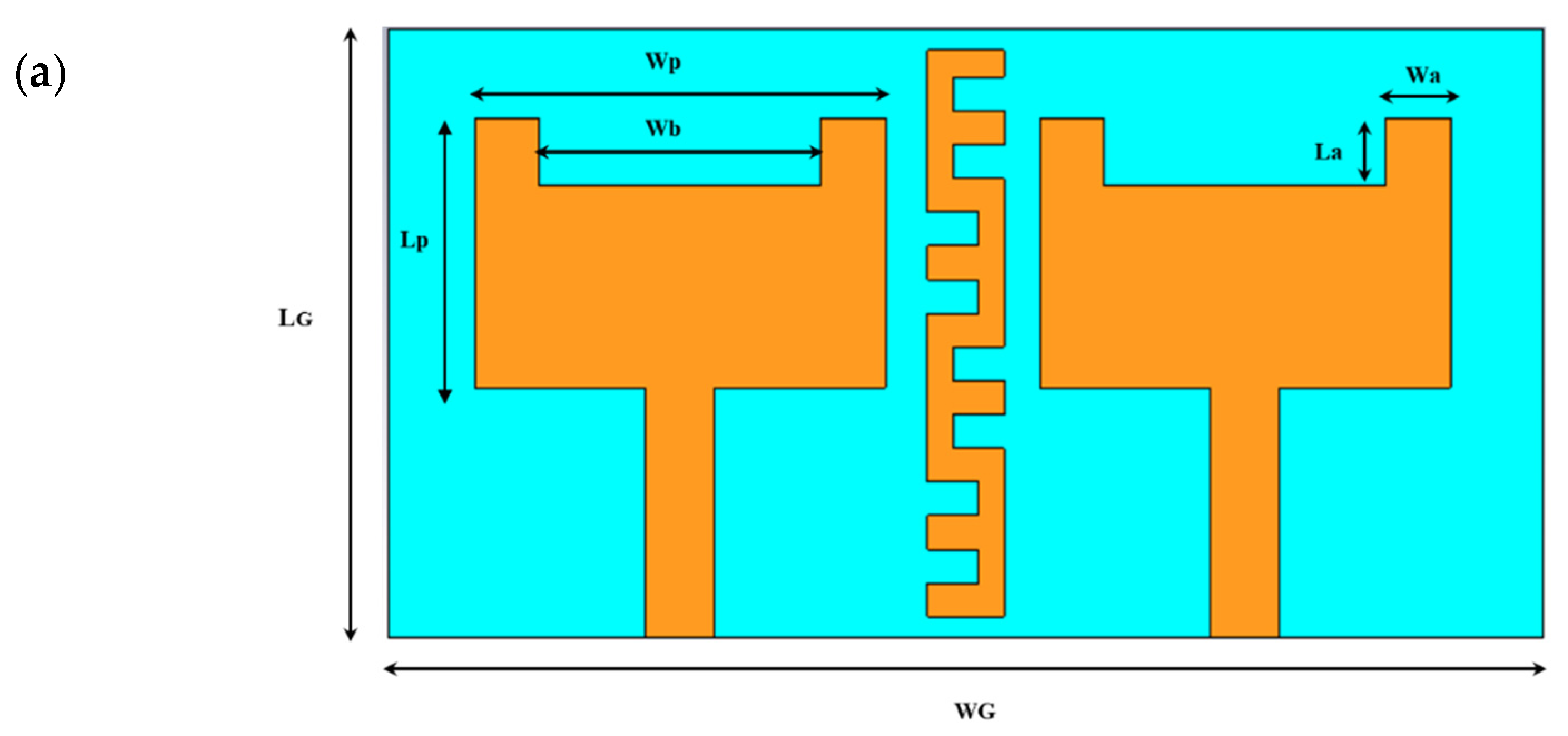
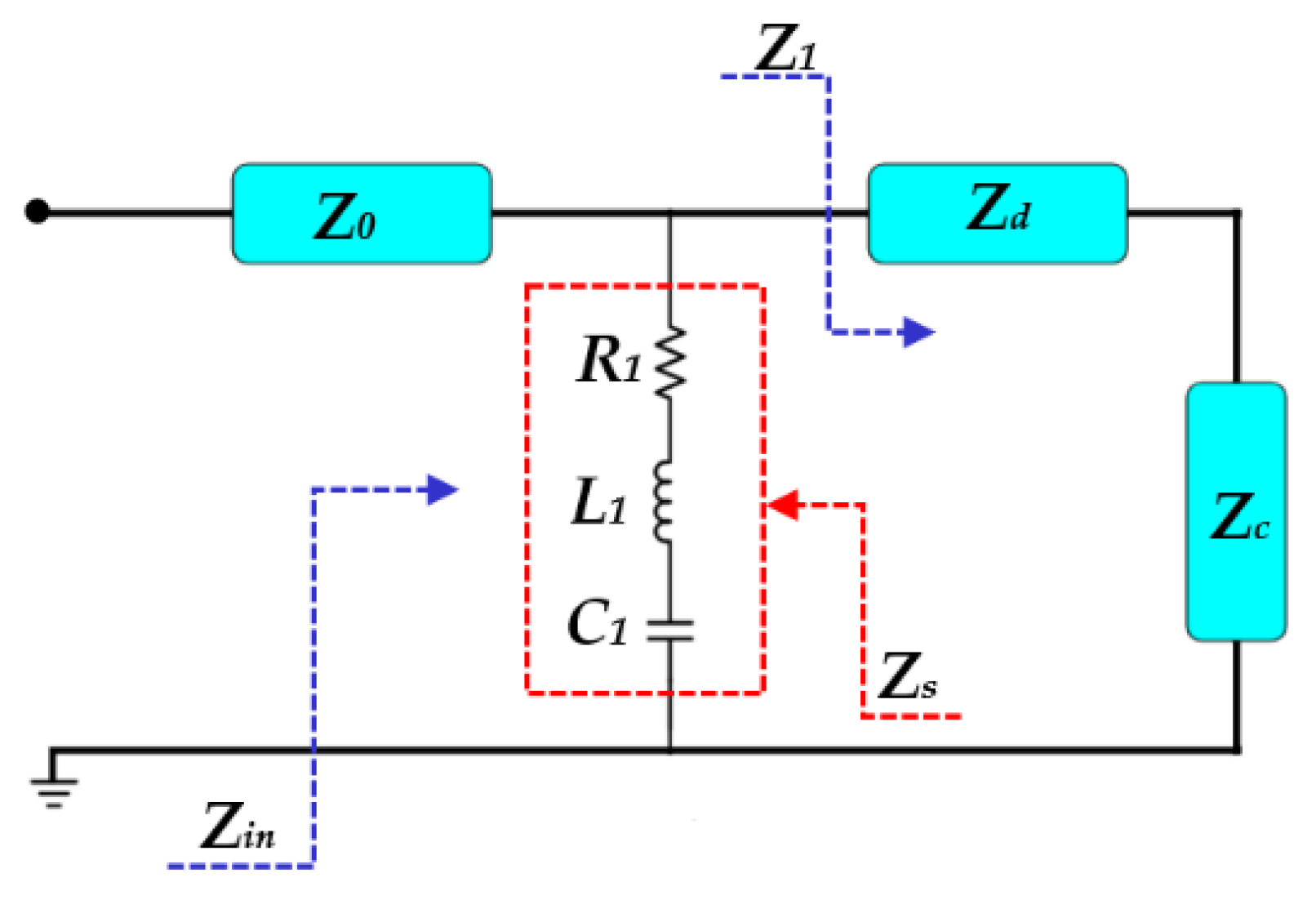
3.2. E-Shaped Metamaterial Unit Cell for Mutual Coupling Reduction

Mutual coupling is the main problem facing MIMO configuration structures. The degree of coupling is determined by the distance between the components. So, the metamaterial structure is a good candidate that is to be used to increase the isolation between the graphene MIMO patches [24]. The new E-shaped metamaterial unit cell introduced between the patches has a band rejection feature (Band-Stop Filter) as presented in Figure 5a. The S-parameters of the metamaterial structure as illustrated in Figure 5b, reveals that the proposed E-shaped metamaterial has a high band-stop characteristic in the desired bandwidth. The metamaterial unit cell has been printed above the substrate between the two patches with a negative value of the relative permittivity and permeability (εr and µr) in the desired bandwidth, which is considered the main condition for the metamaterial design procedure as illustrated in Figure 5c,d.
The proposed E-shaped metamaterial unit cell incorporated between the radiating patches consists of a series four elements connected in opposite manner as indicated in Figure 6a. The E-shaped series has a good impact on the isolation between the elements and, reduces the mutual coupling as shown in Figure 6b. This figure presents a comparison with and without the usage of the E-shaped metamaterial unit cell. It is revealed that the S21 of the antenna (isolation coefficient) decreased from −35 dB to −54 dB. The equivalent circuit model (ECM) of the proposed graphene plasmonic MIMO antenna design with the E-shaped metamaterial unit cell is designed using the ADS software. The ECM is used to validate the results of the CST and compare them. The proposed circuit design of the antenna and S-parameters are listed in Figure 7a,b. The ECM of the antenna consists of a two-input port with 50 Ω input impedance and is separated by the RLC that represents the E-shaped metamaterial resonator. The S-parameters of the antenna reveals that ADS circuit model results are in good agreement and coincide with the CST results with a small deviation due to the values of the RLC components.

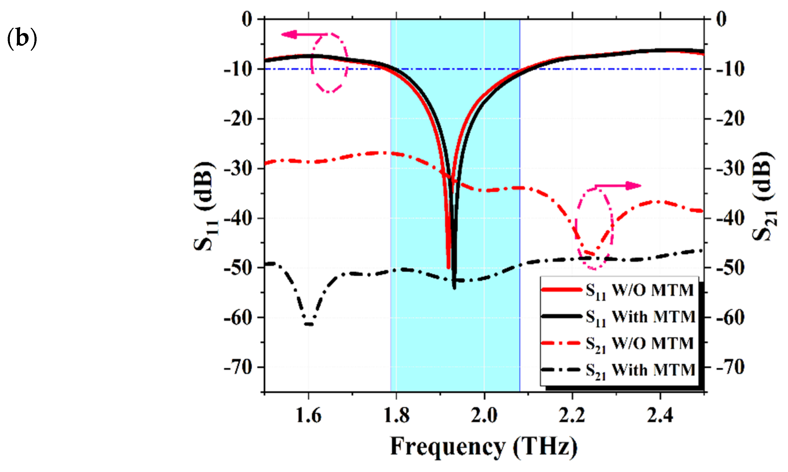
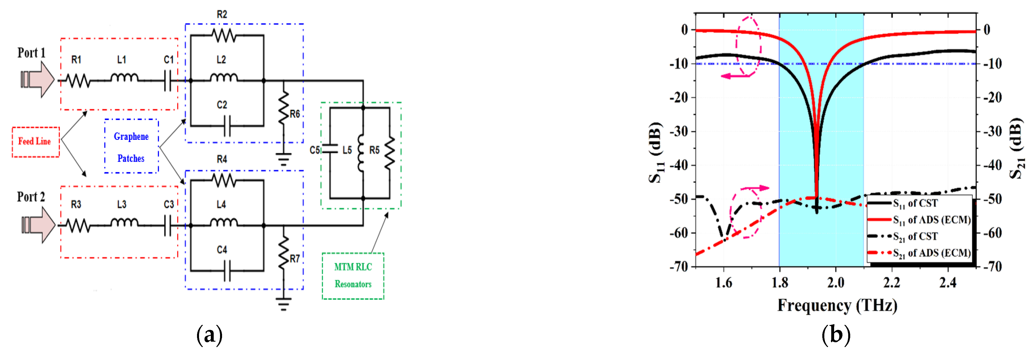
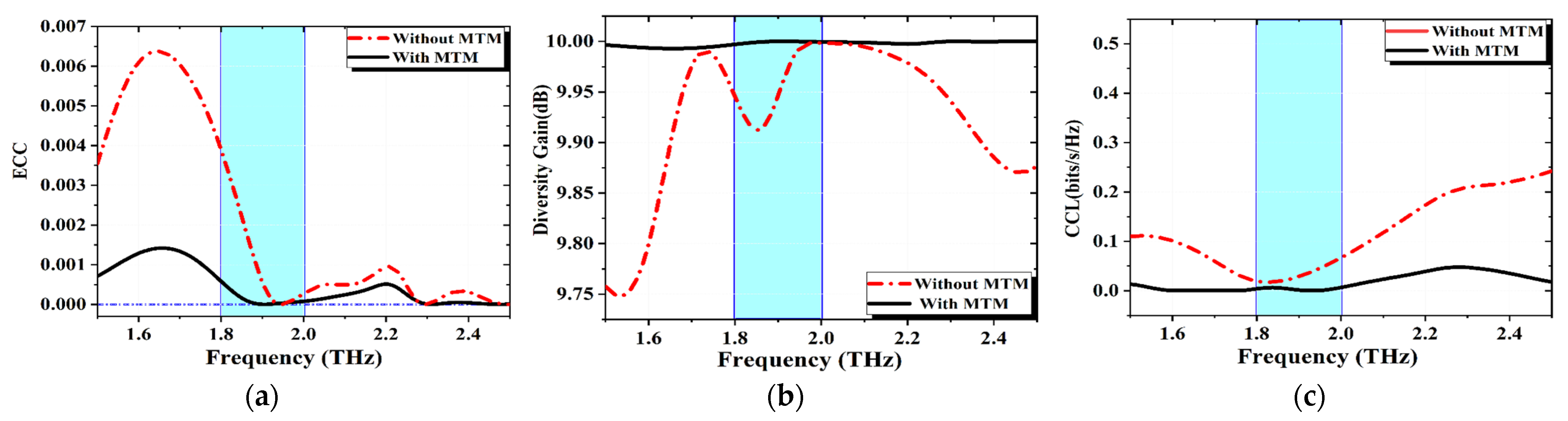
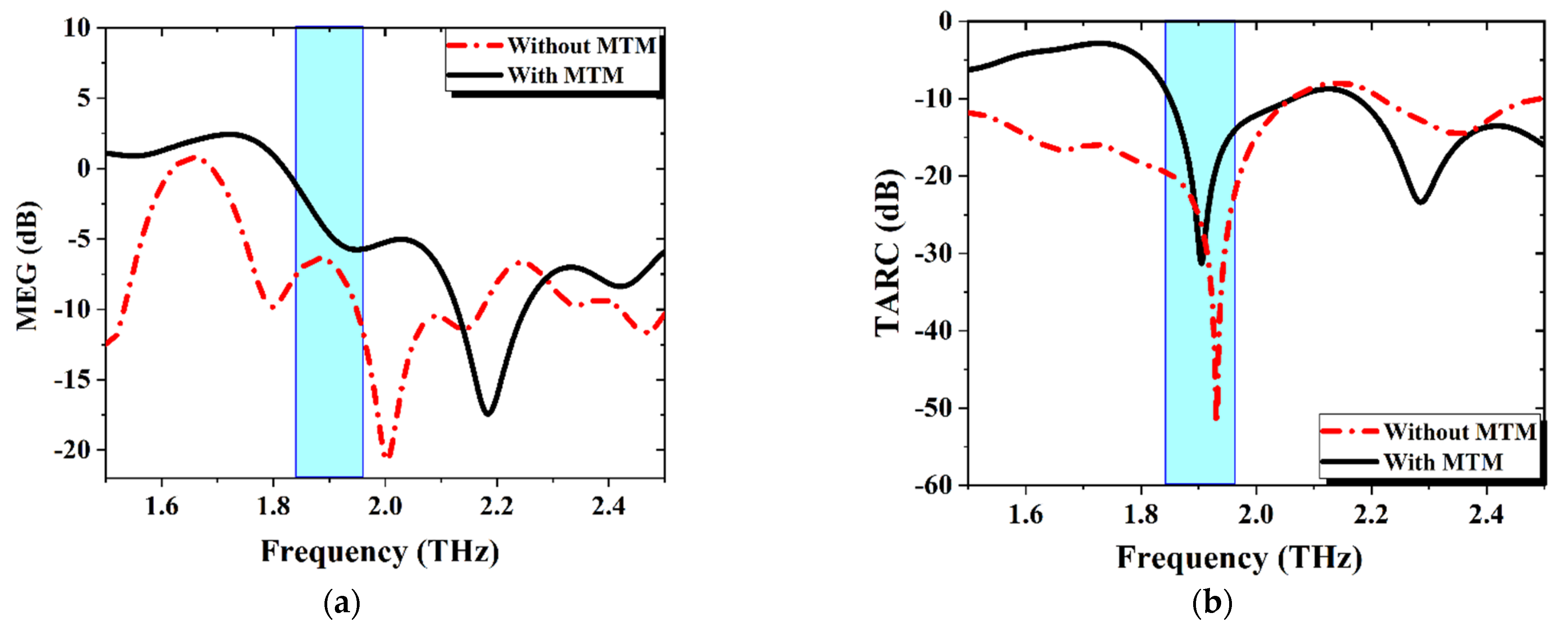
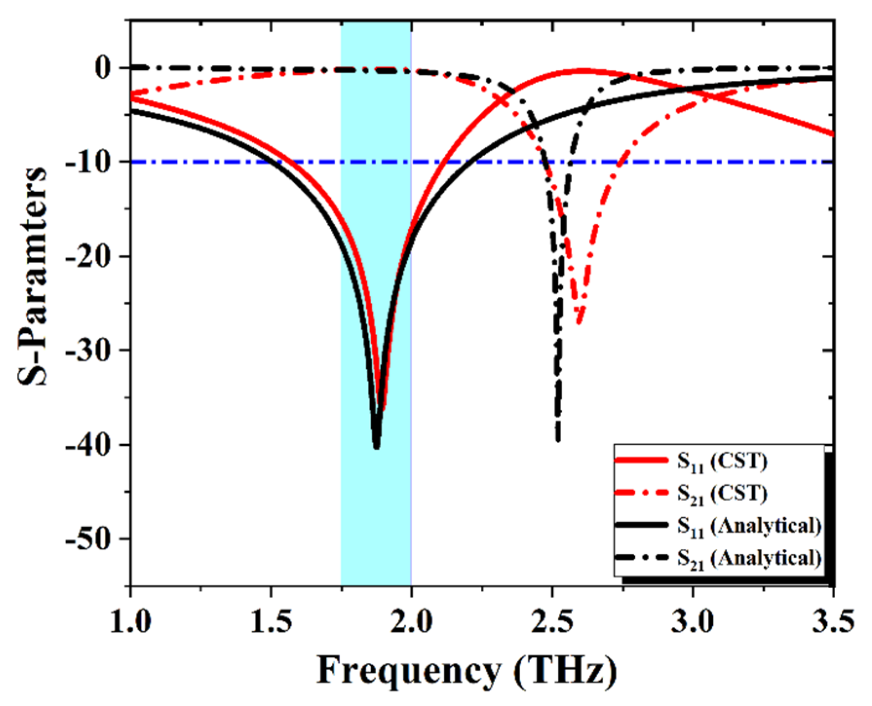
3.3. MIMO Antenna Performance Analysis

Herein in this part, we introduced a discussion and analysis of the most important parameters of the graphene plasmonic MIMO antenna. The envelope correlation coefficient (ECC), diversity gain (DG), and channel capacity loss (CCL) are very crucial parameters in the MIMO systems which reported and discussed in different research papers [16,25]. The ECC is indicates the correlation between the parts of the MIMO antenna configuration. A greater MIMO performance is associated with a smaller amount of ECC between the MIMO components; this value may be determined by the extraction of the S-parameters, as described in [26].
ECC = ρ i j = | S 11 * S 12 + S 21 * S 22 | 2 ( 1 ( | S 11 | 2 + | S 21 | 2 ) ) ( 1 ( | S 22 | 2 + | S 12 | 2 ) )  
where S 11 * and S 21 * represent the conjugate of S 11 and S 21 , respectively. The ECC threshold should be below 0.5 to be considered acceptable. The ECC is computed and shown in Figure 8a for the proposed graphene plasmonic MIMO antenna. In this figure, the value of ECC presented in the absence of the E-shaped metamaterial unit cell has a value of 0.00059, while it has a value of 0.000023 in the presence of the metamaterial through the desired bandwidth. Good MIMO performance of the proposed antenna is ensured by its low ECC value. Diversity gain (DG) reflects power losses in transmission and is another metric that may be used to analyze and assess MIMO antenna performance. The DG can be calculated by using the ECC of the MIMO antenna by following relation [27].
DG = 10 1 ( ECC ) 2  
In the ideal case, in which the value of the ECC = 0, introducing a DG = 10 dB Consequently, for the real case, the ECC value should be extremely small so that the DG must be approximately reached to 10 dB for our proposed MIMO design that is presented in Figure 8b, the diversity gain value is 9.93 dB and 9.999 dB in the presence and absence the MTM unit cell., respectively.
The channel capacity loss (CCL) an essential characteristic for MIMO antenna setups is the channel capacity loss (CCL). The channel impairments caused by inter-MIMO correlation are being revealed. Within the working frequency range, a well-designed MIMO arrangement will have a value of less than 0.5 (bits/s/Hz). As mentioned in, the CCL may be found in Equation (8) [28]:
CCl = log 2 ( φ R )
φ R = [ ρ 11 ρ 12 ρ 21 ρ 22 ]  
ρ i i = ( 1 ( | S i i | 2 + | S i j | 2 ) )     and     ρ i j = ( S i i * S i j + S i j * S j j )
where φ R indicates the correlation matrix at the receiving antenna. A comparison between the CCL curves in the presence and absence the E-shaped metamaterial unit cell is illustrated in Figure 8c. Its value varying from of 0.0014 and 0.028, respectively. It can be confirmed that the suggested design of graphene plasmonic MIMO configuration increases transmission data rates in any scattering environment. The mean effective gain (MEG) is one of the MIMO antenna parameters that is used to measure the average power that is received by the antenna in the fading environment relative to the sum of the average power that can be gained from two isotropic antennas, MEG is calculated from the following relation [29].
MEG = 0.5 ( 1 j = 1 M | S i j | 2 )
where M is the number of MIMO elements. The value of MEG should be less than −3 dB and should be greater than −12 dB. Figure 9a illustrates that the value of MEG is in an acceptable range in the presence and absence of the MTM unit cell. The radiation performance of the MIMO antenna is represented by the total active reflection coefficient (TARC) [30]. It can be calculated using the following relation and introduced in Figure 9b:
TARC = | S 11 + S 12 e j θ | 2 + | S 21 + S 22 e j θ | 2 2  

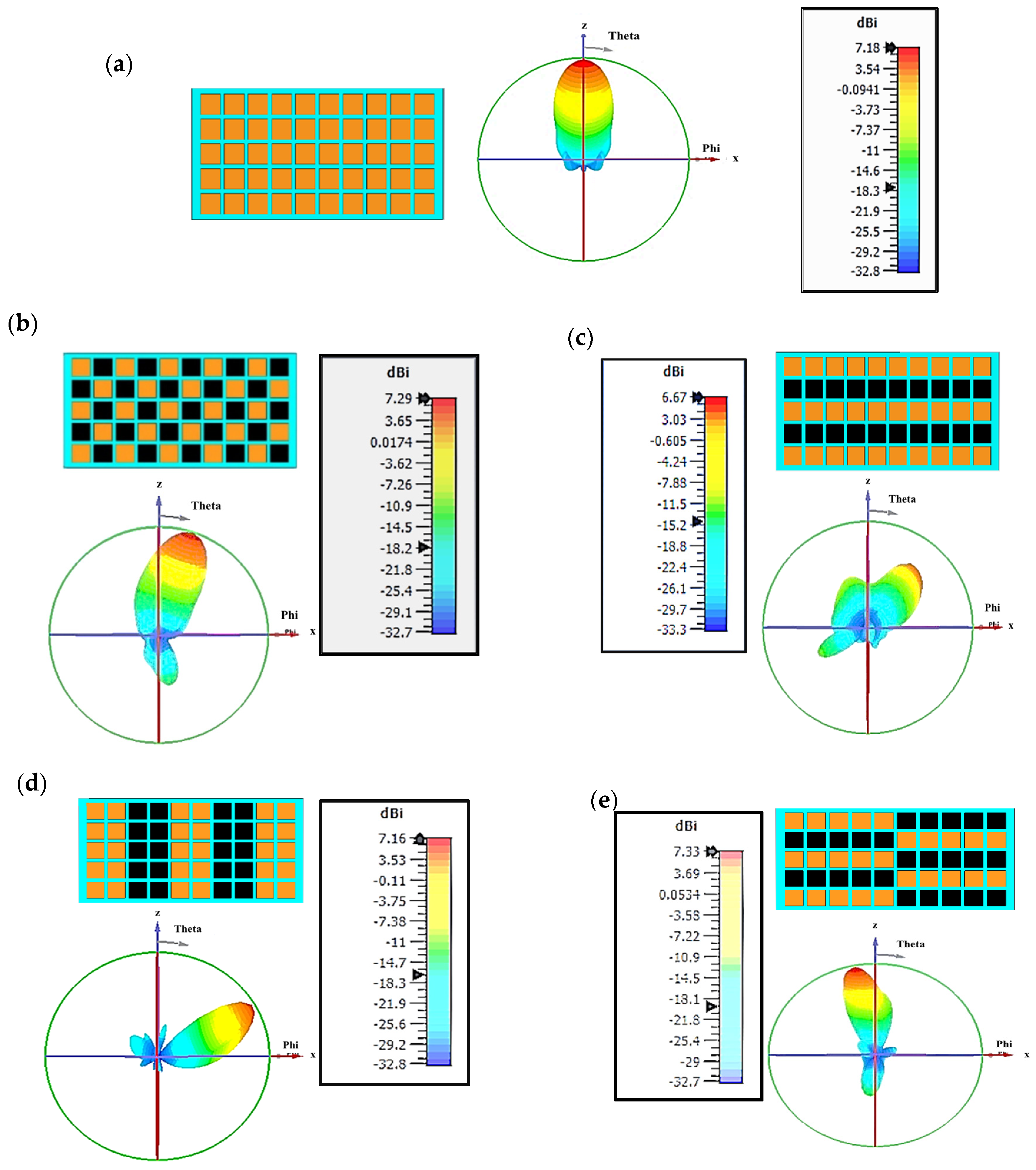
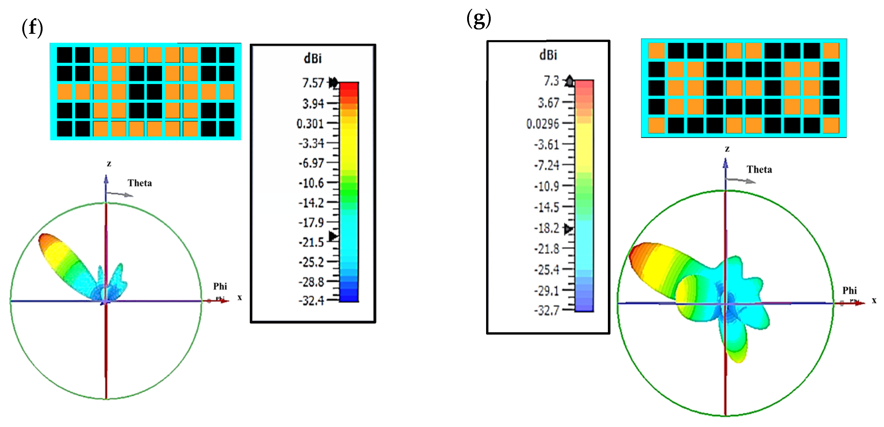
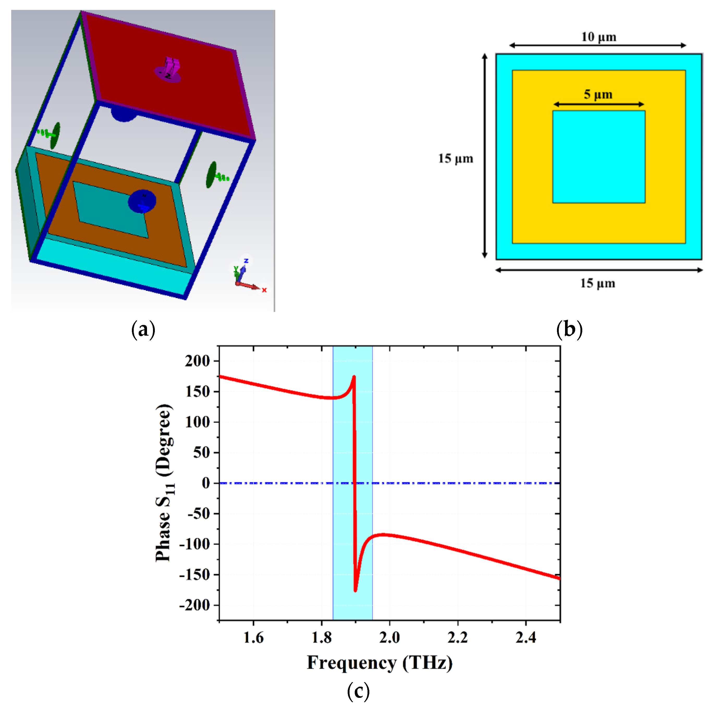
3.4. THz Graphene Reconfigurable Intelligent Surfaces (G-RIS) Design and Analysis

The importance of the RIS appeared in a plethora of applications, especially in the 6G (THz) wireless communication systems. The RIS consists of a periodic structure of meta-atoms (unit cells) that can impose an independent phase shift/amplitude on the impinging THz electromagnetic signal in a fully customized. The phase shift imposed on the THz signal can be adjusted by variations in the wireless propagation environment. By judiciously tuning the phase shifts of the RIS, the signals which reradiated from the RIS layer can be added to other signal paths in a constructive way to enhance the received signal power at the desired users or can be combined in a destructive way to mitigate the unwanted signals at the eavesdroppers. These functionalities push the researcher in the last few years to use the RIS in the 6G wireless communication in the THz frequency band to improve the channel rank, mitigate the channel interference, enhance the system reliability, and position accuracy improvement [31].
A graphene plasmonic meta-atoms as a smart conducting RIS layer is investigated to operate in the THz frequency band. The usage of the graphene material with the reconfigurable intelligent surfaces (G-RIS) added a new degree of freedom in the reconfigurability process. The reconfigurability of the proposed structure of G-RIS in this work is easily achievable by modifying artificially the meta-atoms geometry. An ON/OFF switching behavior of the graphene material is induced by the external gate voltage V g . High conductivity in the graphene layer follows the higher biasing voltage. In contrast, the lower biasing voltage reducing interns the graphene conductivity. The dichotomy between the higher and lower conductivity of the graphene is conceived as an ON/OFF switching state, respectively. The proposed implemented design of the G-RIS is called a reprogrammable meta-tom or a coding meta surface due to its reconfigurability. The G-RIS design consists of a 2D graphene meta-atoms periodic array structure placed upon a polyamide material with a substrate height (h) of 5 µm. The proposed graphene material is modeled in CST microwave studio with a specific parameter. It’s modeled as a thin conductive sheet with a thickness of t g = 0.345   nm , at room temperature of 300 K, fermi energy velocity v f = 10 6   m / s , and free carrier mobility of μ g = 10000   cm 2 /   Vs [32]. The G-RIS is easily reconfigured by applying the biasing gate voltage V g throughout the graphene chemical potential that ranges from μ c = [ 0.1 0.5 ]   eV .
The geometry of the proposed G-RIS is schematically shown in Figure 10a,b in which the top layer of the graphene meta-atoms is periodically arranged with a period of D = 12 µm and a gap of g = 4 µm separated the meta-atoms conductive patches. The G-RIS unit cell shown in Figure 8, illustrates that the bottom layer is a perfect electric conductor (PEC) that is used as a ground plate with a thickness of t p = 0.345   nm . The whole structure of the G-RIS can be modeled as an electrical circuit element based on the transmission line theory. In pursuit of presenting the circuit model description, the graphene meta-atoms are modeled as a thin sheet with a surface impedance of Z s = 1 σ s . The surface conductivity of the graphene layer listed in Equation (1) can be expressed in the Drude model form:
σ s = σ o 1 + j ω τ  
where:
σ o = e 2 K B T π 2 [ μ c K B T + 2 ln ( e μ c / K B T + 1 ) ]
In Figure 11, the equivalent circuit diagram is consisting of (R-L-C) that represents the Z s of the array of graphene meta-atoms, Z d is the impedance of the dielectric layer, Z o = 120   π   Ω which indicates the impedance of the free space, Z c is the impedance of the ground layer of (PEC) that has a conductivity high enough to be considered a short circuit in the THz frequency band so Z c = 0 [33] Based on the electromagnetic wave theory, the reflection coefficient S11 of the proposed G-RIS can be numerically calculated using the following relation:
Γ i n = S 11 = Z i n Z o Z i n Z o  
The total impedance Z i n can be identified by calculating at first the value of the Z 1 with the normal incident THz wave which can be derived in:
Z 1 = Z d Z c + j Z d tan ( β d h ) Z d + j Z c tan ( β d h )  
where Z d is the dielectric impedance,   β d is the propagation constant of the propagating THz wave through the dielectric substrate, and h , is the height of the substrate layer. In the absence of the PEC impedance Z c = 0 , so this relationship can be modified to be:
Z 1 = j Z d tan ( β d h )  
The total input impedance of the proposed G-RIS can be calculated as Z i n = ( Z s Z 1 ) . So, the surface impedance of the array graphene patch can be calculated as in:
Z s = D ( D g ) σ s j π ω ε 0 ( ε r + 1 ) D l n [ csc ( π h 2 D ) ]    
where D is the G-RIS periodicity, g is the distance between the meta-atoms, ε r is the relative permittivity of a substrate. The above equation can be rewritten as [34]:
Z s = D ( D g ) σ s j 1 ω C e f f
where C e f f is the effective capacitance established from the gaps between the meta-atoms of graphene [35]
C e f f = 1 π ε 0 ( ε r + 1 ) D l n [ csc ( π h 2 D ) ]
By insertion of the Drude model of graphene conductivity and substitution in Equation (19), so the graphene surface impedance will be in the following form [34]:
Z s = D ( D g ) 1 + j ω τ σ o j 1 ω C e f f
Z s = D ( D g ) σ o + j [ ω τ D ( D g ) σ o 1 ω C e f f ]
The G-RIS structure can be modeled as (R-L-C) circuit. The resistive and conductive part in Equation (22) is due to the graphene meta-atoms while, the capacitive part is due to the gap between the patches, so this part can be concluded as [35]:
R = D ( D g ) σ o ,                             L = ω τ D ( D g ) σ o ,                           C = C e f f  
So, the total impedance can be calculated from the following relation:
1     Z i n = 1 Z s + 1 Z 1  
According to the (R-L-C) value and the setup parameters of the G-RIS structure, the reflection coefficient S11 can be calculated analytically using the MATLAB program and compared with the results with the electromagnetic solver CST microwave studio. The S-parameter curves are depicted in Figure 12. It reveals that the analytical method has very close results with the CST. So, according to the high impact of the G-RIS structure, it will be a good candidate to be immersed in the whole structure of the superstrate MIMO antenna as illustrated in the next section.

3.5. MIMO Antenna with G-RIS Superstrate Structure

Recent years have witnessed immense research efforts dedicated to improving the overall performance of the RIS to be used in the new technology of the 6G. For the high-demand IoT which hoped to be the internet of intelligence. So, RIS is a good candidate that obeys its requirements. The artificial intelligence RIS is used in a plethora of applications such as healthcare, robotics, unmanned aerial vehicles (UAVs), smart sensors, smart agriculture, self-driving cars, and IoT smart home systems [36]. In this section, we introduced the conventional plasmonic graphene MIMO antenna structure with the addition of a smart and reconfigurable (Coded) superstrate layer of G-RIS meta-atoms. The reconfigurability of the graphene-based intelligent structure layers provokes the G-RIS is suitable for a wide variety of communication scenarios. This layer is placed upon the MIMO antenna as depicted in Figure 13. Herein, we studied the behavior of the G-RIS on the performance of the MIMO antenna structure. The reconfigurability process of the G-RIS is studied and presented from the point of view of frequency and radiation pattern. Firstly, reconfiguring the operating frequency of the main structure (MIMO antenna metasurface G-RIS). The presence of the graphene material gives us the chance to reconfigure the operating frequency of the antenna by varying the graphene chemical potential μ c = [ 0.1 0.5 ]   eV throughout changing the electrical gate voltage. As mentioned before, increasing the value of the chemical potential leads to shifting the operating frequency to higher values. Secondly, the reconfigurable process for the radiation pattern of the antenna. The main functionalities of the G-RIS consist of the beam-steering reconfiguration to provide the line of sight (LOS) user to be used in indoor IoT applications. This property is achieved by modifying the state of the graphene meta-atoms from ON/OFF states (“0” and “1”) that constitute the G-RIS reconfigurable metasurfaces as illustrated in Figure 13. The ON/OFF states of the graphene meta-atoms can be handled by external control of field programmable gate array (FPGA) by dynamically controlling the applying graphene biasing voltage. The programmable G-RIS for a beam steering in a certain direction. So, the order of the meta-atoms must be changed in a specific sequence to achieve the desired direction, so the optimal coding arrangement gives a maximum gain in the optimal direction.
According to our proposed G-RIS programable meta surface, there are a lot of structures that can be achieved by changing the meta surface code to get the desired radiation pattern to the suitable direction. For this property, the G-RIS is a good candidate for point -to multipoint applications which need high directive and narrow beam width patterns. The directive beams will reduce power consumption, especially in the THz IoT applications. The main functionality of the G-RIS beam steering is employed to extend the coverage area of the antenna to increase the number of communication devices. Additionally, it is requisite for alleviating the path interference, in contrast, increasing the gain and directivity of the antenna. The reconfigurability process of the beam steering has a vital role in averting obstacles in the communication system by mitigating noise and interference, improving the security system, increasing the gain, and reducing the power consumption (power saving problems) by directing the transmitted signals to only the desired direction. In our proposed design, the beam-steering mechanism depends on the meta surface operating code. There are many coded G-RISs which produce a variety of paths according to the angle orientation. These different paths are used in smart IoT applications as illustrated in Figure 14 [37]. Figure 15 illustrates the suitable configuration of the G-RIS after a parametric analysis to get the three configurations namely zero-degree orientation, right, and left orientation. All these configurations depend on the (ON/OFF) states of the graphene meta-atoms which interns, which position the radiation pattern in a certain direction. In our proposed structure, the beam steering is approximately from (±60°). This can be noticed well in Figure 16 which illustrates the dependency of the beam steering on the different angle orientation.
Although the idea of coding metamaterials was first proposed for use with microwaves, it has now been effectively applied to other frequencies, including THz and acoustic waves. The beam-steering capability throughout the G-RIS meta-atoms is introduced by the far-field radiation pattern F ( θ ,   Φ ) which can be expressed as [38].
  F ( θ ,   Φ ) = f E ( θ ,   Φ ) × A F ( θ ,   Φ )  
where θ   and   Φ are the elevation and azimuth angle of a certain direction, respectively. f E ( θ ,   Φ ) is the pattern function of a lattice and A F ( θ ,   Φ ) is the array factor for a 2D configuration [38].
A F ( θ ,   Φ ) = n = 1 N m = 1 M A n m e j β n m . e j K o ( x n m sin θ c o s Φ + y n m s i n θ s i n Φ )
where the double summation indicates the positions of row and column meta-atom of 2D array configuration, n = [ 1 , 2 , , N ] and m = [ 1 , 2 , M ] represent the number of elements in row and column, respectively, A n m is the amplitude of each cell, K o = 2 π / λ o is the free space wave number, β n m represents phase excitation between the elements, x n m and y n m denote the position of the unit cell along the x-axis and y-axis, respectively. Herein we consider the graphene coded RIS possibility to characterize the states ON and OFF the graphene meta-atoms that match the bits 0 and 1 digitally. The beam-steering scenario according to the variation of the angle from (±60°) can be adjusted by varying the code of the meta-atom unit cells. According to MATLAB code (1001100….) and the far-field radiation pattern, we can demonstrate the efficiently coded metasurfaces in the proposed direction which can be verified by the CST microwave studio and indicates the optimum order of the G-RIS unit cell for the beam-steering mechanism.

3.6. Suggested MIMO/G-RIS Antenna with AMC Layer

Our proposed design of the graphene plasmonic MIMO antenna configuration with the RIS meta surface has a low operating gain of around 4.5 dB. To enhance the gain of the structure with a directional pattern without increasing the antenna size (conventional methods), an artificial magnetic conductor (AMC) is introduced. The proposed AMC unit cell is illustrated in Figure 17a,b. It is composed of a square patch with an internal square slotted on its center to make a resonance frequency at 1.9 THz on the top layer while a full ground plane is incorporated in the bottom. The resonance frequency of the AMC changes by varying the size of the unit cell. The substrate material is the same used in the MIMO antenna with a thickness of 5 µm. The conducting material of the AMC is carried out by graphene (G-AMC). Figure 17c indicates that the S11 reflection phase of the G-AMC is around 00 throughout the operating frequency of the antenna. For the MIMO antenna structure, the G-AMC layer is at the bottom with a 15 µm separated distance between them. The array size is chosen based on a high-parametric study.
The graphene MIMO antenna structure with the G-RIS superstrate layer is placed above the G-AMC layer. There are three suggested arrays 12 × 12, 10 × 10, and 8 × 8 of unit cells. These three designs are selected and studied to cover the suggested antenna. The main target from the usage of the G-AMC layer is to increase the gain of the MIMO antenna by increasing the array size while the reflection coefficient S11 is not affected due to the array size. The 3D radiation pattern of the proposed design is illustrated in Figure 18. The 12 × 12 G-AMC layer recorded a high gain of 10 dBi, while the 10 × 10, and 8 × 8 structures give a gain of 8.6 and 7.3 dBi, respectively. The 2D curves of the gain assure the same results as depicted in Figure 19 The back surface field direction of the MIMO antenna structure is reflected due to the presence of the G-AMC unit cells through the operating frequency. The reflected waves are collected and added in phase with the main radiated antenna waves which intern enhances the overall gain of the antenna.
The proposed graphene plasmonic MIMO antenna is sandwiched between the G-RIS superstrate layer (at the top) and the G-AMC layer (at the bottom). This mechanism is considered the best choice to enhance the overall gain of the MIMO antenna, furthermore, make the reconfigurability process at the same time. The results of the final proposed design of the three parts (Antenna, G-RIS, and G-AMC) are compared with the states of the arts of the latest published papers on this point. This reveals that the proposed design of the MIMO antenna has a good impact with a suitable result that can be used in different applications such as IoT. The comparison of the proposed antenna with the states of the is of different resent papers are tabulated in Table 2 which reveals that the proposed antenna structure is interested and can be used in different applications of the THz frequency band.

4. Conclusions

Herein In this paper, a graphene MIMO microstrip patch antenna has been introduced for THz wireless communication applications. E-shaped metamaterial unit cells have been placed between the radiating patches to enhance the isolation from −35 dB to −54 dB. The proposed RIS layer based on graphene meta-atoms is placed above the radiating patches to configure the gain to steer at a specific angle (±60°). Another layer based on graphene material is employed to increase the gain of the antenna from 4.5 dBi to 10 dBi, namely G-AMC layers. This layer is placed underneath the antenna at a suitable separated distance. The proposed MIMO antenna is considered a good candidate to be used in a plethora of applications. Due to the high performance of the proposed antenna design it can be used in the high-speed short-distance indoor communication applications (IoTs) which can be used in smart home which need a high gain, high data rate, and beam-steering property to reconfigure the different devices in the smart IoT application Additionally, this proposed antenna can be used in the radar applications which need a wide scanning angle (beam-steering property) to detect the objects in addition to the higher data rate. So, the proposed structure is very interesting design for the THz applications.

Author Contributions

S.A.K. came up with the idea, drafted the paper, and ran the simulations, E.K.I.H. and N.O.P. reviewed the article and carried out the theoretical analysis; N.O.P. and M.B.S. analyzed the numerical findings. S.A.K. and E.K.I.H. enhanced the updated version of the manuscript and contributed to the simulation result and the validation. All authors have read and agreed to the published version of the manuscript.

Funding

This research received no external funding.

Institutional Review Board Statement

Not applicable.

Informed Consent Statement

Not applicable.

Data Availability Statement

All the data have been included in the study.

Conflicts of Interest

No conflict of interest.

References

  1. Krishan, R.J.T.W.C.C.; Technologies, S. Terahertz Band for Wireless Communication—A Review. In Terahertz Wireless Communication Components and System Technologies; Ghzaoui, M.E., Das, S., Lenka, T.R., Biswas, A., Eds.; Springer: Singapore, 2022; pp. 153–161. [Google Scholar] [CrossRef]
  2. Malhotra, I.; Singh, G. Terahertz Technology for Biomedical Application. In Terahertz Antenna Technology for Imaging and Sensing Applications; Springer: Cham, Switzerland, 2021; pp. 235–264. [Google Scholar] [CrossRef]
  3. Civas, M.; Akan, O.B. Terahertz wireless communications in space. ITU J. Futur. Evol. Technol. 2021, 2, 31–38. [Google Scholar] [CrossRef]
  4. Ranaweera, A.L.A.K.; Pham, T.S.; Bui, H.N.; Ngo, V.; Lee, J.-W. An active metasurface for field-localizing wireless power transfer using dynamically reconfigurable cavities. Sci. Rep. 2019, 9, 11735. [Google Scholar] [CrossRef] [Green Version]
  5. Pfeiffer, C.; Grbic, A. Metamaterial Huygens’ Surfaces: Tailoring Wave Fronts with Reflectionless Sheets. Phys. Rev. Lett. 2013, 110, 197401. [Google Scholar] [CrossRef] [PubMed] [Green Version]
  6. Abouelatta, M.A.A.; Obayya, S.S.A.; Hameed, M.F.O. Highly efficient transmissive metasurface for polarization control. Opt. Quantum Electron. 2021, 53, 87. [Google Scholar] [CrossRef]
  7. Wu, C.-T.M.; Chen, P.-Y. Low-Profile Metamaterial-Based Adaptative Beamforming Techniques. In Modern Printed-Circuit Antennas; IntechOpen: London, UK, 2020. [Google Scholar] [CrossRef]
  8. Zhang, X.; Deng, R.; Yang, F.; Jiang, C.; Xu, S.; Li, M. Metasurface-Based Ultrathin Beam Splitter with Variable Split Angle and Power Distribution. ACS Photon. 2018, 5, 2997–3002. [Google Scholar] [CrossRef]
  9. Zhu, X.-F.; Lau, S.-K. Perfect anomalous reflection and refraction with binary acoustic metasurfaces. J. Appl. Phys. 2019, 126, 224504. [Google Scholar] [CrossRef]
  10. Wang, X.; Ding, J.; Zheng, B.; An, S.; Zhai, G.; Zhang, H. Simultaneous Realization of Anomalous Reflection and Transmission at Two Frequencies using Bi-functional Metasurfaces. Sci. Rep. 2018, 8, 1876. [Google Scholar] [CrossRef]
  11. Liaskos, C.; Nie, S.; Tsioliaridou, A.; Pitsillides, A.; Ioannidis, S.; Akyildiz, I. A New Wireless Communication Paradigm through Software-Controlled Metasurfaces. IEEE Commun. Mag. 2018, 56, 162–169. [Google Scholar] [CrossRef] [Green Version]
  12. Li, Y.; Lin, J.; Guo, H.; Sun, W.; Xiao, S.; Zhou, L. A Tunable Metasurface with Switchable Functionalities: From Perfect Transparency to Perfect Absorption. Adv. Opt. Mater. 2020, 8, 1901548. [Google Scholar] [CrossRef]
  13. Dash, S.; Patnaik, A.; Letters, O.T. Material selection for TH z antennas. Microw. Opt. Technol. Lett. 2018, 60, 1183–1187. [Google Scholar] [CrossRef]
  14. Ghaffar, A.; Li, X.J.; Awan, W.A.; Hussain, N. Reconfigurable Antenna: Analysis and Applications. In Wideband, Multiband, and Smart Antenna Systems; Springer: Berlin/Heidelberg, Germany, 2021; pp. 269–323. [Google Scholar] [CrossRef]
  15. Karthika, K.; Kavitha, K. Reconfigurable Antennas for Advanced Wireless Communications: A Review. Wirel. Pers. Commun. 2021, 120, 2711–2771. [Google Scholar] [CrossRef]
  16. Khaleel, S.A.; Hamad, E.K.I.; Parchin, N.O.; Saleh, M.B. MTM-Inspired Graphene-Based THz MIMO Antenna Configurations Using Characteristic Mode Analysis for 6G/IoT Applications. Electronics 2022, 11, 2152. [Google Scholar] [CrossRef]
  17. Ojaroudi, M.; Loscri, V. Graphene-Based Reconfigurable Intelligent Meta-Surface Structure for THz Communications. In Proceedings of the 2021 15th European Conference on Antennas and Propagation (EuCAP), Düsseldorf, Germany, 22–26 March 2021; pp. 1–5. [Google Scholar] [CrossRef]
  18. Fazaelifar, M.; Jam, S.; Basiri, R. A circular polarized reflectarray antenna with electronically steerable beam and interchangeable polarizations. Int. J. Microw. Wirel. Technol. 2020, 13, 198–210. [Google Scholar] [CrossRef]
  19. Geim, A.K.; Novoselov, K.S. The rise of graphene. In Nanoscience and Technology; Co-Published with Macmillan Publishers Ltd.: British, UK, 2009; pp. 11–19. [Google Scholar]
  20. Beiranvand, B.; Sobolev, A.S.; Sheikhaleh, A. A proposal for a dual-band tunable plasmonic absorber using concentric-rings resonators and mono-layer graphene. Optik 2020, 223, 165587. [Google Scholar] [CrossRef]
  21. Gómez-Díaz, J.S.; Perruisseau-Carrier, J. Graphene-based plasmonic switches at near infrared frequencies. Opt. Express 2013, 21, 15490–15504. [Google Scholar] [CrossRef]
  22. Khaleel, S.A.; Hamad, E.K.I.; Saleh, M.B. High-performance tri-band graphene plasmonic microstrip patch antenna using superstrate double-face metamaterial for THz communications. J. Electr. Eng. 2022, 73, 226–236. [Google Scholar] [CrossRef]
  23. Vakil, A.; Engheta, N. Transformation Optics Using Graphene. Science 2011, 332, 1291–1294. [Google Scholar] [CrossRef] [Green Version]
  24. Roshani, S.; Shahveisi, H. Mutual Coupling Reduction in Microstrip Patch Antenna Arrays Using Simple Microstrip Resonator. Wirel. Pers. Commun. 2022, 126, 1665–1677. [Google Scholar] [CrossRef]
  25. Khan, M.I.; Khan, S.; Kiani, S.H.; Parchin, N.O.; Mahmood, K.; Rafique, U.; Qadir, M.M. A Compact mmWave MIMO Antenna for Future Wireless Networks. Electronics 2022, 11, 2450. [Google Scholar] [CrossRef]
  26. Zahra, H.; Awan, W.; Ali, W.; Hussain, N.; Abbas, S.; Mukhopadhyay, S. A 28 GHz Broadband Helical Inspired End-Fire Antenna and Its MIMO Configuration for 5G Pattern Diversity Applications. Electronics 2021, 10, 405. [Google Scholar] [CrossRef]
  27. Naqvi, S.I.; Hussain, N.; Iqbal, A.; Rahman, M.; Forsat, M.; Mirjavadi, S.S.; Amin, Y. Integrated LTE and Millimeter-Wave 5G MIMO Antenna System for 4G/5G Wireless Terminals. Sensors 2020, 20, 3926. [Google Scholar] [CrossRef] [PubMed]
  28. Hussain, N.; Jeong, M.-J.; Abbas, A.; Kim, N. Metasurface-Based Single-Layer Wideband Circularly Polarized MIMO Antenna for 5G Millimeter-Wave Systems. IEEE Access 2020, 8, 130293–130304. [Google Scholar] [CrossRef]
  29. Hussain, N.; Awan, W.A.; Ali, W.; Naqvi, S.I.; Zaidi, A.; Le, T.T. Compact wideband patch antenna and its MIMO configuration for 28 GHz applications. AEU—Int. J. Electron. Commun. 2021, 132, 153612. [Google Scholar] [CrossRef]
  30. Raj, U.; Sharma, M.K.; Singh, V.; Javed, S.; Sharma, A. Easily extendable four port MIMO antenna with improved isolation and wide bandwidth for THz applications. Optik 2021, 247, 167910. [Google Scholar] [CrossRef]
  31. Pan, C.; Zhou, G.; Zhi, K.; Hong, S.; Wu, T.; Pan, Y.; Ren, H.; Di Renzo, M.; Swindlehurst, A.L.; Zhang, R.; et al. An Overview of Signal Processing Techniques for RIS/IRS-Aided Wireless Systems. IEEE J. Sel. Top. Signal Process. 2022, 16, 883–917. [Google Scholar] [CrossRef]
  32. Novoselov, K.S.; Geim, A.K.; Morozov, S.V.; Jiang, D.; Zhang, Y.; Dubonos, S.V.; Grigorieva, I.V.; Firsov, A.A. Electric field effect in atomically thin carbon films. Science 2004, 306, 666–669. [Google Scholar] [CrossRef] [Green Version]
  33. Aghaee, T.; Orouji, A.A. Reconfigurable multi-band, graphene-based THz absorber: Circuit model approach. Results Phys. 2019, 16, 102855. [Google Scholar] [CrossRef]
  34. Padooru, Y.R.; Yakovlev, A.B.; Kaipa, C.S.R.; Hanson, G.W.; Medina, F.; Mesa, F. Dual capacitive-inductive nature of periodic graphene patches: Transmission characteristics at low-terahertz frequencies. Phys. Rev. B 2013, 87, 115401. [Google Scholar] [CrossRef]
  35. Liu, Z.; Guo, L.; Zhang, Q. Design of Dual-Band Terahertz Perfect Metamaterial Absorber Based on Circuit Theory. Molecules 2020, 25, 4104. [Google Scholar] [CrossRef]
  36. Das, S.K.; Benkhelifa, F.; Sun, Y.; Abumarshoud, H.; Abbasi, Q.H.; Imran, M.A.; Mohjazi, L. Comprehensive Review on ML-based RIS-enhanced IoT Systems: Basics, Research Progress and Future Challenges. TechRxiv 2022. [Google Scholar] [CrossRef]
  37. IoT—Internet of Things. Things. Interactive Demos of the Smart Connected Kitchen of the Future at NRF 2017. 2017. Available online: https://iot.do/interactive-demos-smart-connected-kitchen-nrf-2017-01 (accessed on 14 November 2022).
  38. Babu, K.V.; Das, S.; Varshney, G.; Sree, G.N.J.; Madhav, B.T.P. A micro-scaled graphene-based tree-shaped wideband printed MIMO antenna for terahertz applications. J. Comput. Electron. 2022, 21, 289–303. [Google Scholar] [CrossRef]
  39. Jarchi, S. Radiation pattern direction control of THz antenna with applying planar graphene metasurface. Optik 2021, 243, 167458. [Google Scholar] [CrossRef]
  40. Shubham, A.; Samantaray, D.; Ghosh, S.K.; Dwivedi, S.; Bhattacharyya, S. Performance improvement of a graphene patch antenna using metasurface for THz applications. Optik 2022, 264, 169412. [Google Scholar] [CrossRef]
  41. Basiri, R.; Zareian-Jahromi, E.; Aghazade-Tehrani, M. A reconfigurable beam sweeping patch antenna utilizing parasitic graphene elements for terahertz applications. Photon. Nanostructures Fundam. Appl. 2022, 51, 101044. [Google Scholar] [CrossRef]
  42. Babu, K.V.; Das, S.; Sree, G.N.J.; Madhav, B.T.P.; Patel, S.K.K.; Parmar, J. Design and optimization of micro-sized wideband fractal MIMO antenna based on characteristic analysis of graphene for terahertz applications. Opt. Quantum Electron. 2022, 54, 281. [Google Scholar] [CrossRef]
Figure 1. Flowchart of the proposed design.
Electronics 12 00164 g001
Figure 2. Surface conductivity of graphene for different chemical potentials (a) real part and (b) imaginary part.
Electronics 12 00164 g002
Figure 3. The proposed MIMO configurations; (a) side-by-side orientation and (b) orthogonal orientation.
Electronics 12 00164 g003
Figure 4. (a) The S11 of the proposed antenna with different chemical potential and (b) The S11 and S21 of the proposed graphene MIMO configurations.
Electronics 12 00164 g004
Figure 5. The parameters of the MTM unit cell, (a) MTM structure of E-shape, (b) S-parameters of the unit cell, (c) relative permittivity, and (d) relative permeability.
Electronics 12 00164 g005
Figure 6. (a) The proposed structure of the MIMO antenna with metamaterial unit cell and, (b) The S-parameters of the antenna in the presence and absence of metamaterial unit cell.
Electronics 12 00164 g006aElectronics 12 00164 g006b
Figure 7. (a) The ADS equivalent circuit model and, (b) The S-parameters of the antenna using CST and ADS.
Electronics 12 00164 g007
Figure 8. (a) Envelop correlation coefficient (ECC), (b) Diversity gain (DG), and (c) channel capacity loss (CCL) of the proposed antenna in the presence and absence the metamaterial unit cell.
Electronics 12 00164 g008
Figure 9. (a) Mean effective gain (MEG) and (b) total active reflection coefficient (TARC) parameters.
Electronics 12 00164 g009
Figure 10. (a) RIS boundary condition, and (b) RIS with geometrical parameters.
Electronics 12 00164 g010
Figure 11. The equivalent circuit model of G-RIS structure.
Electronics 12 00164 g011
Figure 12. The S-parameters of the proposed G-RIS structure and compered the results with CST and analytical methods.
Electronics 12 00164 g012
Figure 13. MIMO antenna structure with the G-RIS superstrate meta-atoms.
Electronics 12 00164 g013
Figure 14. G-RIS for indoor wireless IoT applications.
Electronics 12 00164 g014
Figure 15. Gain orientation of the proposed MIMO antenna with different configurations of G-RIS meta-atoms (a) Zero-degree orientation, (bd) Positive orientation and (eg) Negative orientation.
Electronics 12 00164 g015aElectronics 12 00164 g015b
Figure 16. Beam-steering orientation with different angles value.
Electronics 12 00164 g016
Figure 17. AMC unit cell (a) The applied boundary condition (b) 2D layout with optimized dimensions, and (c) the Simulated S11 reflection phase of the AMC unit cell.
Electronics 12 00164 g017
Figure 18. Different AMC configurations (a) 8 × 8, (b) 10 × 10, and (c) 12 × 12-unit cells with different gain values.
Electronics 12 00164 g018
Figure 19. The 2D gain values of the MIMO antenna for different AMC configurations.
Electronics 12 00164 g019
Table 1. The proposed antenna parameters.
Par.Value (µm)Par.Value (µm)
Ws120Ls90
Wp65Lp40
Wf10Lf35
Wa8La8
Wb49WG180
d25
Two Element Parameters of ADS Circuit
R1 = R3 = R6 = R725.8 ΩL1 = L37.15 pH
C1 = C30.7 fFL2 = L410 pH
C2 = C41.48 fFR2 = R4 = R560.3 Ω
L50.8 pHC50.5 fF
Table 2. Comparison with the state-of-the-art works.
Ref.Freq. (THz)Size (µm2)Decoupling MethodMax. Isolation Improvement (dB)Gain (dBi)ECC/DG (dB)CCLReconfigurabilityAntenna Configuration
[39]0.4935600 × 300Separated Distance−404.740.001/9.950.00018-MIMO
[16]3.5130 × 85MTM + Elements Arrangement−557.230.000168/9.9990.006-MIMO
[40]1.2192 × 192--4.26--Gain reconfigurable + Metasurfaces
(±35°)
Single element
[41]2.02256 × 216--8.91--Gain reconfigurable + Graphene Metasurfaces
(±50°)
Single element
[38]1.47422 × 359--4.88–7.68--Gain reconfigurable + Graphene ribbons
(30°:150°)
Single element
[42]0.51600 × 300Separated Distance−545.490.015/9.99-Frequency reconfigurable + Graphene chemical potentialMIMO
Proposed Work1.9120 × 90MTM+
AMC
−544.5–100.000023/9.990.0014-Frequency reconfigurable Graphene chemical potential. —Gain reconfigurable + Graphene RIS (±60°)MIMO
Disclaimer/Publisher’s Note: The statements, opinions and data contained in all publications are solely those of the individual author(s) and contributor(s) and not of MDPI and/or the editor(s). MDPI and/or the editor(s) disclaim responsibility for any injury to people or property resulting from any ideas, methods, instructions or products referred to in the content.

