Article

Integrated 0.35-µm CMOS Control Circuits for High-Performance Voltage Mode DC–DC Boost Converter

School of Electrical and Computer Engineering, Chungbuk National University, Cheongju 28644, Republic of Korea
*
Authors to whom correspondence should be addressed.
Electronics 2023, 12(1), 133; https://doi.org/10.3390/electronics12010133
Submission received: 23 November 2022 / Revised: 21 December 2022 / Accepted: 23 December 2022 / Published: 28 December 2022

Abstract

:
The integrated DC–DC converter is appropriate for use in many domains, namely, display, cellular, and portable applications. This paper presents an integrated control circuit for a monolithic voltage mode DC–DC boost converter for display driver applications. The control circuits consist of a transconductance amplifier, a comparator, and an oscillator. The boost converter consists of an inductor, two MOSFET, and an output RC filter. The control circuits are designed for fast transient response and low output ripple. The transconductance amplifier, comparator, and oscillator in the control circuit are designed to operate at a supply voltage of 3.3 V and an operating frequency of 5.5 MHz. The transconductance amplifier consists of an operational amplifier and an RC filter in the feedback path. The RC filter has a pole with a sufficient phase margin for high stability. The control circuits are realized in a 0.35-μm CMOS process together with the DC–DC converter. The fabricated DC–DC converter was evaluated by experiment and simulation. Testing of the proposed control circuits shows that the output transient time can be controlled within 7 μs, and the output voltage is accurately controlled with a ripple ratio of 3%.

1. Introduction

In this paper, we present a low-power system on a DC–DC boost converter for display driver applications. There have been intensive research efforts on CMOS-integrated DC–DC boost converters for low-power applications. Lai and co-workers have proposed a 0.18-um CMOS device design of a 0.6–1.7 V boost converter using a 2.3-GHz oscillator and two differential cross-coupled rectifiers [1]. Chang and co-workers have a single-inductor multi-output (SIMO) DC–DC converter 0.18-um 1P6M CMOS process for converting 1.8 V to 1.5, 2.0, 2.2, 2.5 V [2]. They employed two comparator loops and two error amplifier loops. Jiang and co-workers investigated a buck-boost converter with 0.22–2.4 V input and 0.85–1.2 V output employing an algorithmic voltage-feed-in topology [3]. Choi and co-workers presented a soft-switching hybrid DC–DC converter realized in a 65-nm CMOS process [4]. They achieved 79.5% efficiency. Guierrez proposed a fully-integrated DC–DC converter for IoT power supply applications [5]. He achieved 69% peak efficiency with 180-nm bipolar CMOS-DMOS technology. Song and co-workers studied a switched-capacitor DC–DC step-up converter for implantable neural interface applications [6]. They achieved 82.6% efficiency with a 180 nm CMOS 1P6M process.
In DC–DC converters, the converter consists of a power stage and a control stage. The control stage requires an op-amplifier [7,8,9] for low-power operation and high accuracy. The op-amplifier accurately controls the drain-source voltage of the power transistor. This control circuit [10,11,12] is a high-gain amplifier in a differential pair.
In this paper, we propose integrated control circuits for a high-performance DC–DC boost converter for display applications. While current mode control [13,14] is much better than voltage mode control, there are a lot of difficulties in the implementation of the current sensing circuit. In a voltage-mode DC–DC converter, the performance of the voltage control circuit is crucial to the converter’s performance. The aim of this paper is to develop fully integrated control circuits for high-performance DC–DC boost converters for 3.3-V input and 5 to 7-V output voltage operation. The proposed control circuits work on the pulse width modulation principles and consist of an operational transconductance amplifier (OTA) or compensator, a comparator, a 5.5-MHz oscillator, and a gate driver. In the design of the control circuits, the main focus is on a fast response to load change or a short transient time and a low ripple in the output voltage. Each sub-circuit in the control circuits is designed for the overall objectives of fast response and low ripple voltage based on the 0.35-μm CMOS process.
The structure of the proposed voltage-mode boost converter consists of a power stage and a control stage, as shown in Figure 1. A converter usually consists of a power switching stage and a feedback control circuit. Among the variable circuit elements of voltage-mode converters, a transconductance amplifier, a comparator, and an oscillator in the control circuits are critical to the performance of the overall feedback operation, which requires fast dynamic response and reduction in sub-harmonic oscillation. The feedback network is a system-on-integrated circuit for voltage-mode gate driver control. By using the properties of the CMOS transistor, a high-performance control circuit can be manufactured. It enables accurate sensing of the inductor current at high frequency.
The power stage includes two MOS switches MN1, MP1 with an off-chip LC filter. The voltage-mode DC–DC boost converter in a system-on-chip configuration is designed with a 0.35-µm CMOS process for low-power operation and full integration of the circuitry. The input voltage of the op-amplifier is scaled down by R2 and R3. The off-chip LC filter is designed for inductance of 1–10 μH and capacitance of 0.1–1 μF. The control circuit is designed for a supply voltage of 3.3 V and an operating frequency of 5.5 MHz. The operation of the proposed control circuits with the voltage-mode DC–DC boost converter was verified by simulation and by experiments.

2. Control Circuits

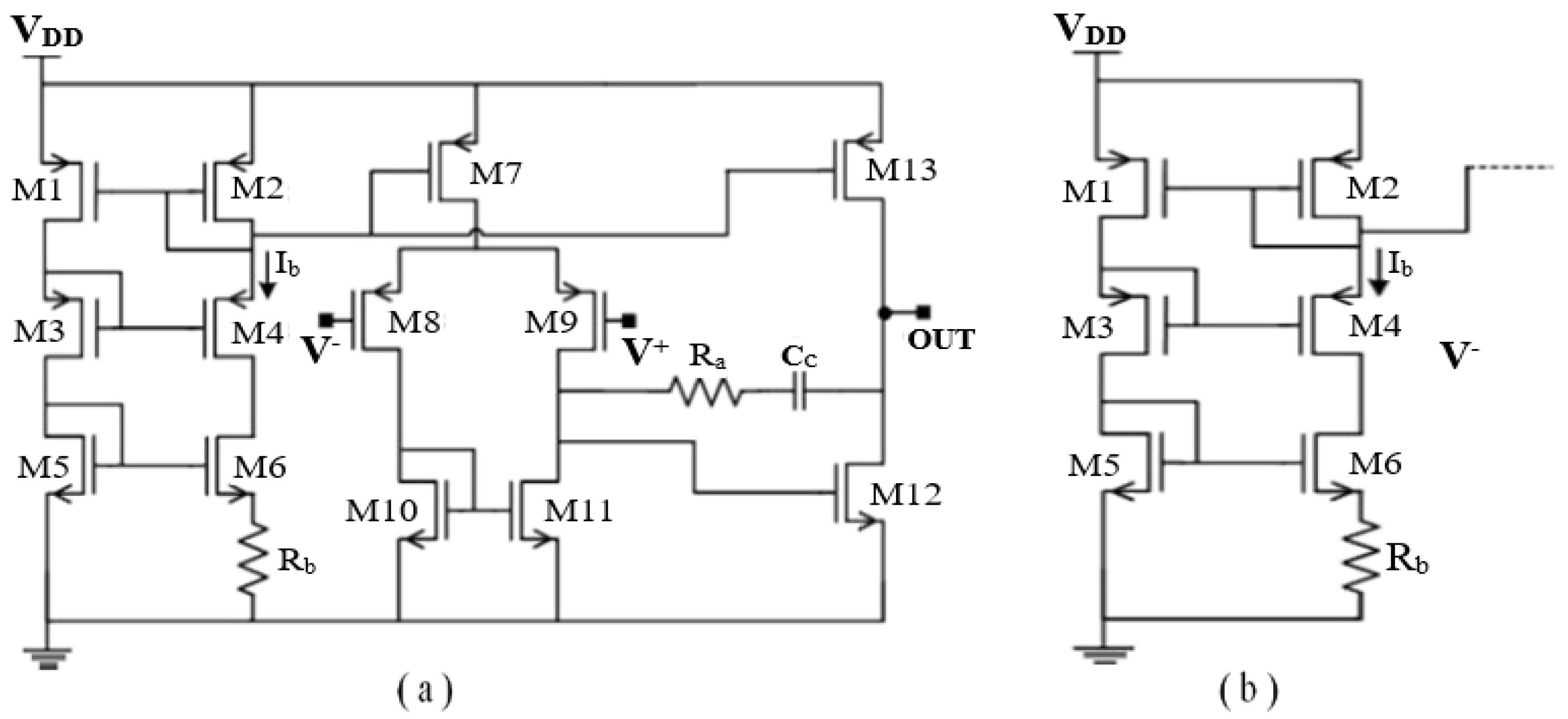
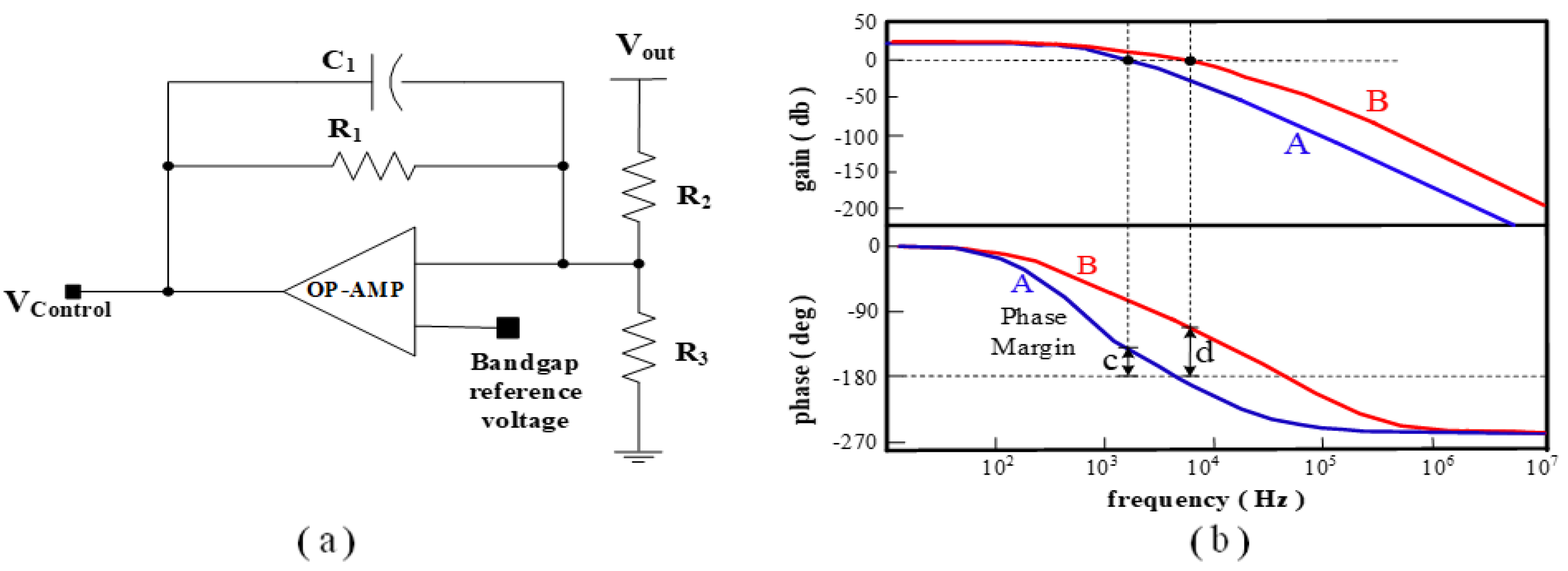
2.1. Operational Transconductance Amplifier (OTA) Circuit

The two-stage operational amplifier configuration is a popular structure for CMOS op-amps, and it has reasonably good quality in addition to the simplicity of the circuit. As seen in Figure 2, the two-stage operational amplifier configuration is composed of a differential amplifier input stage, current sources, and a feedback compensator, which requires a fast-transient response with low-power consumption.
The OTA in Figure 2a consists of an input differential stage, a source follower, and current mirrors. A compensator is included in the op-amp to increase the stability of the frequency response and to achieve a fast response time. A differential amplifier is used in the first stage since it is less sensitive to noise due to its high common mode rejection ratio (CMRR). Although there is only one capacitor Cc, in the negative feedback path of the second stage (frequency-compensated) in the OTA, a resistor Ra in series with CC is used to improve the phase margin of the op-amp by placing zero in the negative axis. It usually includes a compensation circuit to achieve stability of frequency response and fast response time. The compensator is used to realize poles or zeros for a sufficient phase margin for high stability. A drawback of this configuration is that it does not have a low output resistance suitable for driving low input impedance loads. In order to implement IREF current in Figure 2a, the bias circuit in Figure 2b needs to be capable of providing current independent of the supply voltage and the MOSFET threshold voltage. A useful and interesting property of the bias circuit is that the transconductances of the transistors biased by this circuit are only dependent on Rb value and device dimensions. As seen in Figure 2b, a resistor Rb is connected in series with the source of M6. This resistor Rb is important in determining the bias current Ib and the transconductance of the transistor M6.
Figure 3a is an operational amplifier with a compensator. The transfer function of the compensator with poles due to the RC filter [15,16] can be written in the following form by applying Miller’s theorem. The resistors and capacitors are used to create poles or zeros in the compensator, where Aop and Rout are the gain and output resistance of the op-amp, and R1 and C1 are the resistance and capacitance of the compensator.
V c o n t r o l V o u t = k ( 1 + s R 1 C 1 )
f C = 1 2 π R 1 C 1
A S = A O P ( 1 + S / ω P )
ω P = [ R P · C P ] 1
The stability and frequency response are determined directly by the pole. Whether the converter circuit is stable or not can be determined by examining the loop gain as a function of the frequency, where k, R1, and C1 are the gain, resistance, and capacitance in the compensator. The fC is the compensating frequency determined by the resistance R1 and capacitance C1. Figure 3b shows the gain of the compensator versus the frequency, where phase B with pole-zero optimization is shown together with that of case A without pole-zero optimization. In case A, the phase margin (c) is almost 0° while the phase margin (d) is 47°. The frequency characteristic of the compensated op-amplifier is combined into the control feedback loop characteristics of the DC–DC boost converter. The results indicate that the compensator frequency should be higher than the initial unoptimized frequency for increased phase margin and, thus, higher stability. Another factor affecting phase margin and stability is the gain of the op-amplifier given in Equation (3). The op-amplifier is designed to maintain a small quiescent current during normal operation and to withstand large input signal fluctuations. The transconductance of the op-amplifier was well controlled to maintain the stability of the converter.

2.2. Comparator Circuit

The comparator [17,18] in Figure 4a is for the pulse-width modulation (PWM) control. It is composed of a bias circuit, an input differential stage, and a latch. The bias circuit is almost the same as that of the op-amplifier. The input stage is a circuit for start-up and bandgap reference. A start-up circuit is added to ensure that the bandgap reference circuit turns on when the supply voltage is applied. The load circuit employs a current mirror configuration and thus presents an amplifier with a high-resistance load. With this approach, a gain larger than 20 is achievable. The inverter and latch are used for a clear logic response and can act as a driver stage, so transistors in the current mirror can be made smaller for reduced parasitic capacitance.
The operation of the comparator is a simple process. When the compensator op-amplifier output voltage is less than that of the 5.5 MHz triangular waveform voltage, the output voltage of the comparator is low. When the compensator output voltage is greater than the triangle waveform voltage, the output of the comparator is high. Figure 4b shows the output waveforms of the op-amplifier (A) and the comparator (B). This is obtained from the Cadence simulation tool of the block diagram containing the power and control stage circuits. The output of the op-amplifier (A) quickly settles down due to the high conductance gm of the differential pair. The comparator repeats the digital high and low logic until the op-amp signal (A) passes the transient response.

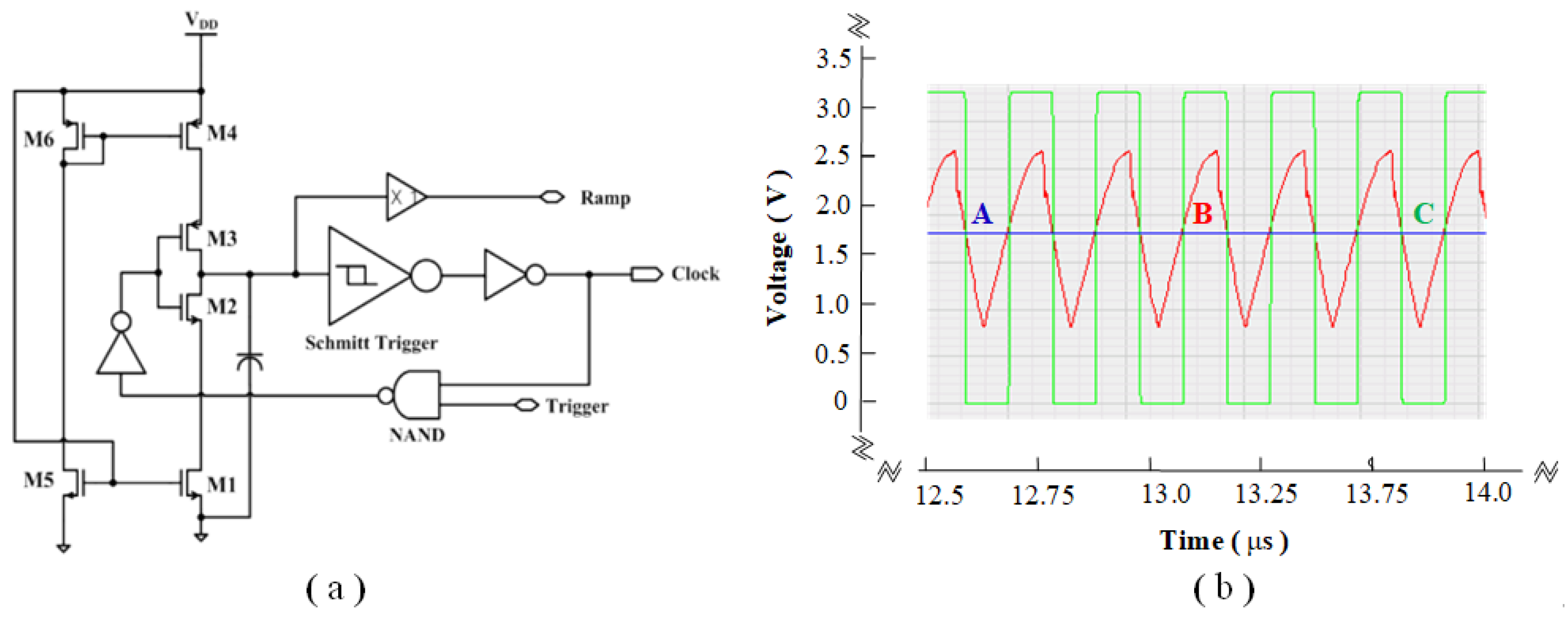
2.3. Oscillator Circuit

An oscillator signal is used for PWM control and for PWM switching [12]. The switch control signal is generated by comparing the compensator op-amp output voltage with a triangular waveform obtained from the oscillator signal. The oscillator circuit is shown in Figure 5a. The oscillator is a sawtooth waveform generator that employs current sources and a Schmitt trigger. The MOSFETs M2 and M3 are used as switches. A Schmitt trigger circuit with a NAND gate is employed to obtain a ramp signal and a clock signal. The signal clock and ramp signal are generated from a trigger signal.
Figure 5b shows the output waveforms of the compensator (A), oscillator (B), and comparator (C). When the compensator output voltage is less than the triangle waveform voltage, the output of the comparator is a low voltage. When the compensator output voltage is greater than the triangle waveform voltage, the output of the comparator is a high voltage.

2.4. Gate Driver Circuit

Figure 6a shows a gate driver circuit. The circuit is connected to power switches MN1 and MP1 mode of power MOSFETs. The driver circuit requires a careful design as it can draw large currents and generate overshoot currents during switching transitions. The gate driver circuit consists of a NAND gate, two NOR gates, and two SR latches. The signals of the ramp (A) and clock (B) are shown in Figure 6b. The duty ratio, frequency, and amplitude can be changed by varying parameters of the oscillator.

3. Results

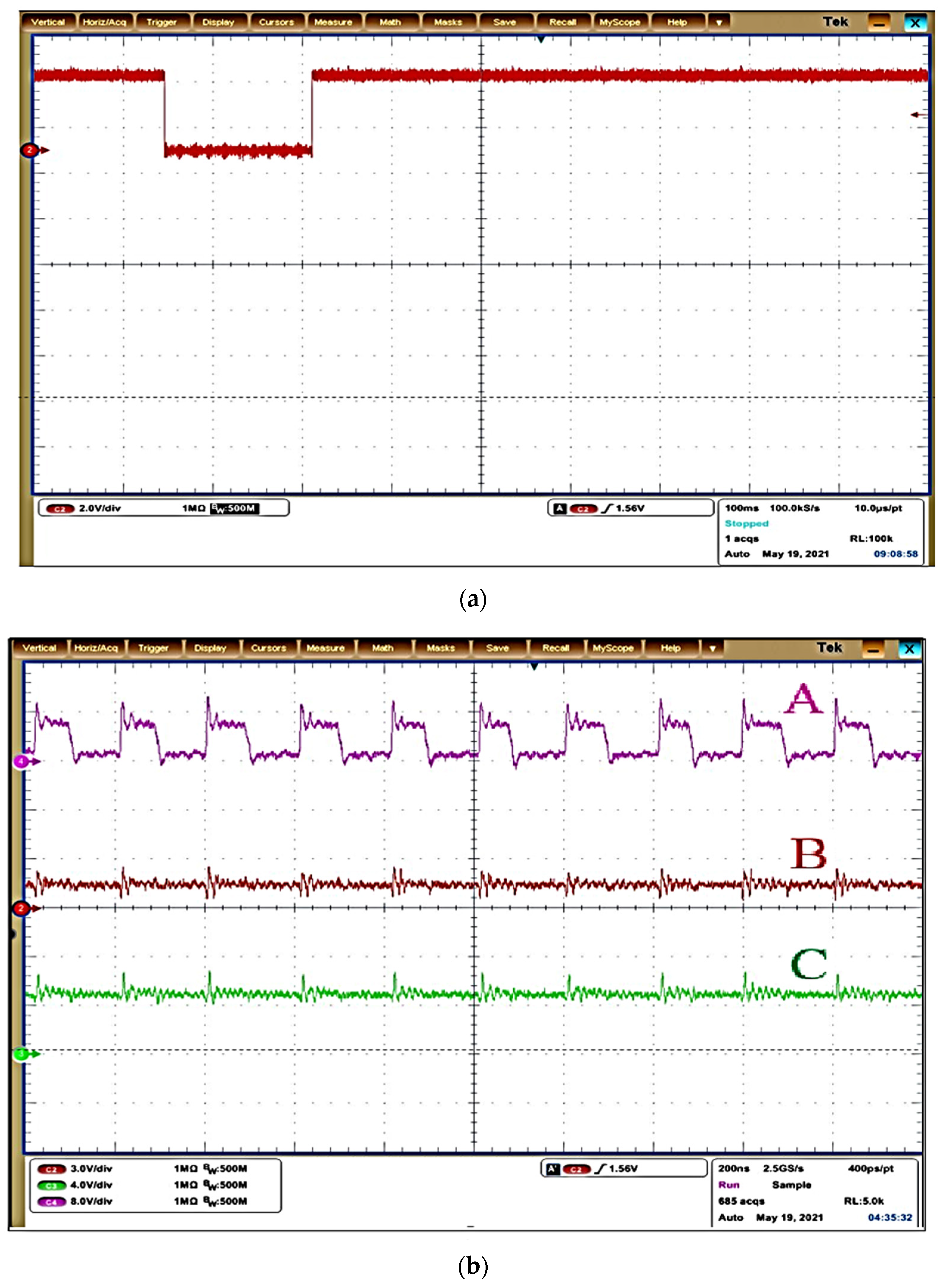
3.1. Results of Simulation and Experiments

The voltage-mode DC–DC converter with an on-chip integrated PWM circuit operates at 5.5 MHz with an input voltage of 3.3 V. The power MOSFET in the power stage is isolated from the control stage to avoid noise. An LC filter is designed with an inductance of 1–10 µH and capacitance of 0.1–1 µF. The simulation result of inductor current IL and inductor voltage VL is shown in Figure 7a. It has been obtained with an input voltage of 3.3 V, inductance of 10 μH, capacitance of 1 μF, and duty ratio of 0.7. The charge and discharge times of the inductor current IL are accurately sensed. The ripple current depends on the output voltage, inductance, and duty ratio. The discharge time is approximately 0.07 μs.
The inductor current is 190 mA within 5% ripple. Figure 7b shows the output and ripple voltages of DC–DC boost converter when they are 6.3 V and 75 mV, respectively. The output voltage has been obtained as expected with a negligible ripple ratio. In LC filter converters, glitches typically occur in the on-off switching transistors in the power stage. The Cadence simulation tool has been used to simulate the converter SoC of Figure 1. The duty cycle of the power switches MN1 and MP1 is approximately 70%.
Figure 8a shows the measured waveform of the input trigger signal and Figure 8b shows the measured waveform of the inductor voltage VL, feedback voltage, and output voltage. The measured output voltage is 5.6 V at a switching frequency of 5.5 MHz. The voltage VL across the inductor shows a high ripple during on-off switching states. The output power is approximately 300 mW. The glitches in the (A), (B), and (C) waveforms are caused by a mismatch in the power switch of the MN1 and MP1 power MOSFETs. It was obtained with an inductor of 10 μH, input voltage of 3.3 V, capacitor of 1 μF, and duty ratio of 0.5.
Figure 9a shows the output voltage and efficiency with a variation of the load current. As the load current increases, the power efficiency is almost constant at 75%, and the output voltage decreases. This indicates that the efficiency is almost independent of the load current in the measured current range. However, when the load resistor becomes smaller with high frequency, the dynamic power loss is relatively larger than the static power loss, and the efficiency can be reduced because of the switching noise. The ripple voltage with a variation of the load current is shown in Figure 9b. The result corresponds to the dependency that can be obtained from Equation (5), and the ripple voltage is proportional to the load current. The ripple voltage is under 80 mV at the load current of 200 mA. Figure 9c shows the output voltage versus duty of the PWM signal. The output voltage linearly depends on the duty cycle, as expected.
V r i p p l e = I o u t f C o u t

3.2. Designed Condition and Photo Die of the Proposed DC–DC Boost Converter

The performance of the proposed voltage-mode DC–DC converter is summarized in Table 1. The proposed DC–DC converter achieves a high figure of merit with a small chip area.
The proposed DC–DC boost converter is designed in 0.35 µm CMOS technology with 2-poly and 4-metal processes as shown in Figure 10.

4. Conclusions

A voltage-mode DC–DC boost converter with full integration is presented in this article. The proposed voltage-mode DC–DC boost converter is designed using 0.35-µm CMOS technology with 2-poly and 4-metal processes. Measurements of the fabricated converter have shown that the converter’s output voltage ranges from 5–7 V with an input voltage of 3.3 V and a PWM switching frequency of 5.5 MHz. The feedback control circuit is applied in order to obtain a small ripple voltage that is almost independent of the load resistance. The feedback circuit operates with an OTA, amplifier, comparator, gate driver circuit, and oscillator. The proposed converter can be used as a miniaturized low-power LED driver IC. The power consumption has been found to be approximately 300 mW with maximum efficiency of ≅77%, which is applicable for high-performance LED display driver circuits. The proposed voltage-mode DC–DC boost converter offers such advantages as a simpler circuit structure than the current-mode converter and superior performance in terms of output voltage and power consumption.

Author Contributions

Conceptualization, C.-S.L., S.-G.C. and B.-C.A.; methodology, M.G. and C.-S.L.; validation, M.G., B.D. and C.-S.L.; formal analysis, C.-S.L., S.-G.C. and B.-C.A.; formal data curation B.D., S.-G.C. and C.-S.L.; writing—original draft, C.-S.L.; writing—review and editing, M.G., S.-G.C., C.-S.L. and B.-C.A. All authors have read and agreed to the published version of the manuscript.

Funding

This research was supported by Basic Science Research Program through the National Research Foundation of Korea (NRF) funded by the Ministry of Education, Science and Technology (grant number: NRF-2020R1I1A1A01066637), by the MSIT (Ministry of Science and ICT), Korea, under the Grand Information Technology Research Center support program (grant number: IITP-2022-2020-0-01462) supervised by the IITP (Institute for Information & communications Technology Planning & Evaluation), and by Basic Science Research Program through the National Research Foundation of Korea (NRF) funded by the Ministry of Education (grant number: 2020R1A6A1A12047945).

Data Availability Statement

Not applicable.

Acknowledgments

The authors would like to thank IDEC for the CAD tool support.

Conflicts of Interest

The authors declare no conflict of interest.

References

  1. Lai, C.W.; Jang, S.L.; Huang, C.Y.; Juang, M.H. Fully-Integrated CMOS DC-DC Boost Converter. In Proceedings of the Asia Power and Energy Engineering Conference(APEEC), Chengdu, China, 23 May 2019; pp. 84–88. [Google Scholar]
  2. Chang, R.H.; Chen, W.C.; Siao, C.H.; Wu, H.W. Low-complexity SIMO buck-boost DC-DC converter for gigascale systems. In Proceedings of the 2016 IEEE International Symposium on Circuits and Systems (ISCAS), Montreal, QC, Canada, 22–25 May 2016; pp. 614–617. [Google Scholar]
  3. Jiang, Y.; Law, M.K.; Mak, P.I.; Martins, R.P. A 0.22-to-2.4V-input fine-grained fully integrated rational buck-boost SC DC-DC converter using algorithmic voltage-feed-in (AVFI) topology achieving 84.1% peak efficiency at 13.2mW/mm2. In Proceedings of the 2018 IEEE International Solid State Circuits Conference(ISSCC), San Francisco, CA, USA, 11–15 February 2018; pp. 422–424. [Google Scholar]
  4. Choi, M.H.; Jeong, D.K. Design of Soft-Switching Hybrid DC-DC Converter with 2-Phase Switched Capacitor and 0.8nH Inductor for Standard CMOS Process. Electronics 2020, 9, 372. [Google Scholar] [CrossRef] [Green Version]
  5. Gutierrez, F. Fully-Integrated Converter for Low-Cost and Low-Size Power Supply in Internet-of-Things Applications. Electronics 2017, 6, 38. [Google Scholar] [CrossRef] [Green Version]
  6. Song, S.M.; Kim, M.S.; Park, S.Y. A Low-Power, Fully Integrated SC DC–DC Step-Up Converter with Phase-Reduced Soft-Charging Technique for Fully Implantable Neural Interfaces. Electronics 2022, 11, 3659. [Google Scholar] [CrossRef]
  7. Hong, S.W.; Park, S.H.; Kong, T.H.; Cho, G.H. Inverting Buck-Boost DC-DC Converter for Mobile AMOLED Display Using Real-Time Self-Tuned Minimum Power-Loss Tracking (MPLT) Scheme with Lossless Soft-Switching for Discontinuous Conduction Mode. IEEE J. Solid-State Circuits 2015, 50, 2380–2393. [Google Scholar] [CrossRef]
  8. Josh, W.; Ramesh, H. A high-efficiency DC-DC converter using 2 nH integrated inductors. IEEE J. Solid-State Circuits 2008, 43, 844–854. [Google Scholar]
  9. Lee, C.S.; Kim, S.S.; Yu, J.H. Load and frequency dependent CMOS dual-mode DC-DC converter. Microelectron. J. 2019, 92, 104610. [Google Scholar] [CrossRef]
  10. Patella, B.J.; Prodić, A.; Zirger, A.; Maksimović, D. High- frequency digital PWM controller IC for DC-DC converters. IEEE Trans. J. Power Electron. 2003, 18, 438–446. [Google Scholar] [CrossRef] [Green Version]
  11. Roh, J. High-performance error amplifier for fast transient DC-DC converters. IEEE Trans. Circuits Syst. II 2005, 52, 591–595. [Google Scholar]
  12. Gendensuren, M.; Park, J.W.; Lee, C.S.; Kim, N.S. Low Power Integrated 0.35um CMOS Voltage-Mode DC-DC Boost Converter. In Proceedings of the 4th International Conference on Power Engineering, Energy and Electrical Drives, Istanbul, Turkey, 13–17 May 2013; pp. 502–505. [Google Scholar]
  13. Leung, C.Y.; Mok Philip, K.T.; Leung, K.N. A 1-V integrated current-mode boost in standard 3.3/5-V CMOS technologies. IEEE J. Solid-State Circuits 2005, 40, 2265–2274. [Google Scholar] [CrossRef]
  14. Lee, C.S.; Kim, N.S.; Gendensuren, M.; Choi, J.H.; Choi, J.H. Integrated on-chip 0.35 µm BiCMOS current-mode DC-DC buck converter. Int. J. Electron. 2012, 99, 1623–1634. [Google Scholar] [CrossRef]
  15. Tao, X.; Xu, J. Integrated current–sensing circuit with offset-current cancellation for boost converters. In Proceedings of the 2008 International Conference on Communications, Circuits and Systems IEEE, ICCCAS, Xiamen, China, 25–27 May 2008; pp. 1328–1331. [Google Scholar]
  16. Lee, C.S.; Ko, H.H.; Kim, N.S. Current-mode DC–DC boost converter with high-performance control circuit. Analog. Integr. Circuits Signal Process. 2014, 80, 105–112. [Google Scholar] [CrossRef]
  17. Reverter, F.; Gasulla, M. Optimal Inductor Current in Boost DC/DC Converters Operating in Burst Mode under Light-Load Conditions. IEEE Trans. Power Electron. 2016, 31, 15–20. [Google Scholar] [CrossRef]
  18. Forghani-zadeh, H.P.; Rincon-Mora, G.A. An accurate, continuous, and lossless self-learning CMOS current sensing scheme for inductor-based DC-DC converters. IEEE J. Solid-State Circuits 2007, 42, 665–679. [Google Scholar] [CrossRef]
Figure 1. Block diagram of the proposed voltage–mode boost DC–DC converter.
Electronics 12 00133 g001
Figure 2. Proposed OTA circuit: (a) two–stage CMOS op–amp configuration; (b) configuration used to bias two–stage op–amp.
Electronics 12 00133 g002
Figure 3. Proposed OTA circuit: (a) schematic of compensator with operational amplifier; (b) frequency response of the loop gain (A: without pole–zero optimization, B: with pole–zero optimzation).
Electronics 12 00133 g003
Figure 4. Proposed comparator circuit: (a) comparator circuit; (b) outputs of the op-amplifier (A) and comparator (B).
Electronics 12 00133 g004
Figure 5. Proposed oscillator circuit: (a) oscillator circuit; (b) output of compensator (A), oscillator (B), and comparator (C).
Electronics 12 00133 g005
Figure 6. Proposed gate driver circuit: (a) gate driver circuit; (b) signals of ramp (A) and clock (B).
Electronics 12 00133 g006
Figure 7. Simulation results: (a) output of inductor current IL (blue) and voltage VL (red) after inductor; (b) output voltage.
Electronics 12 00133 g007
Figure 8. Experiments results: (a) input trigger signal; (b) inductor voltage VL after inductor (A), feedback voltage (B), and output voltage (C). (Scale 0.1 μs/div and 2.0 V/div).
Electronics 12 00133 g008
Figure 9. Test results: (a) output voltage and power efficiency with variation of the load current; (b) ripple voltage with variation of the load current; (c) output voltage versus duty.
Electronics 12 00133 g009
Figure 10. Die photo of the DC–DC boost converter.
Electronics 12 00133 g010
Table 1. Performance summary.
TypeBoost Converter
Process0.35 μm CMOS process
Input voltage (VIN)3.3 V
Output voltage (VOUT)5–7 V
Load current (IL)15–200 mA
Switching frequency (fs)5.5 MHz
Ripple voltage 10–100 mV
Efficiency≅75% (I mA)
Die area size0.5 mm2
Disclaimer/Publisher’s Note: The statements, opinions and data contained in all publications are solely those of the individual author(s) and contributor(s) and not of MDPI and/or the editor(s). MDPI and/or the editor(s) disclaim responsibility for any injury to people or property resulting from any ideas, methods, instructions or products referred to in the content.

