
Current Collapse Conduction Losses Minimization in GaN Based PMSM Drive


Abstract
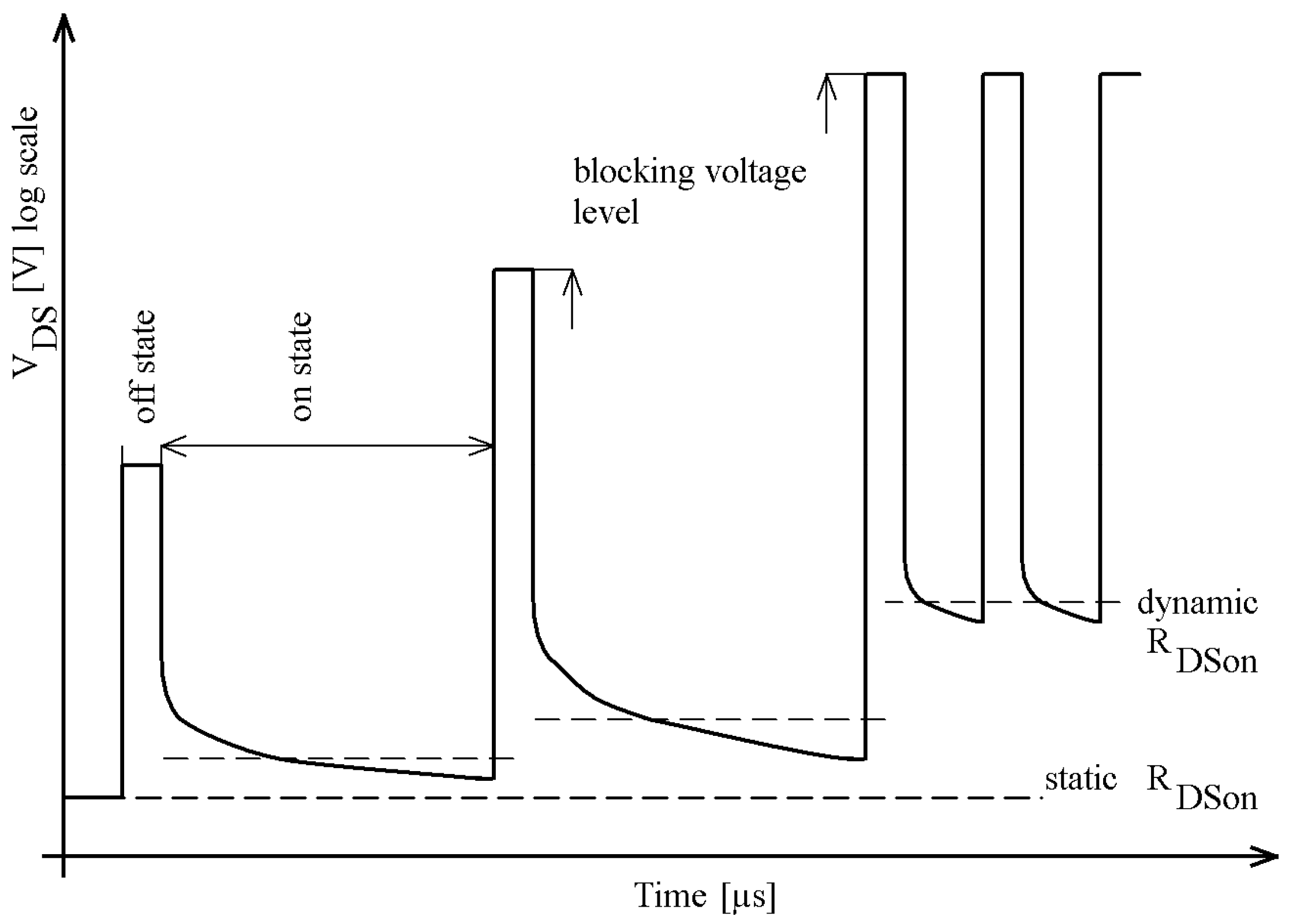
:1. Introduction
2. Theoretical Analysis
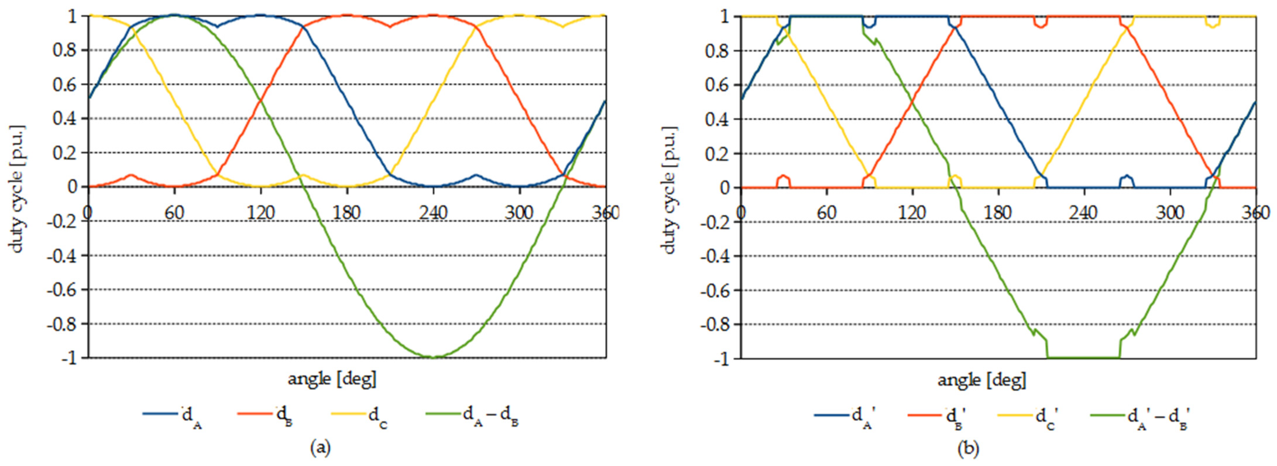
2.1. Space-Vector Modulation with Minimum Pulse Limitation
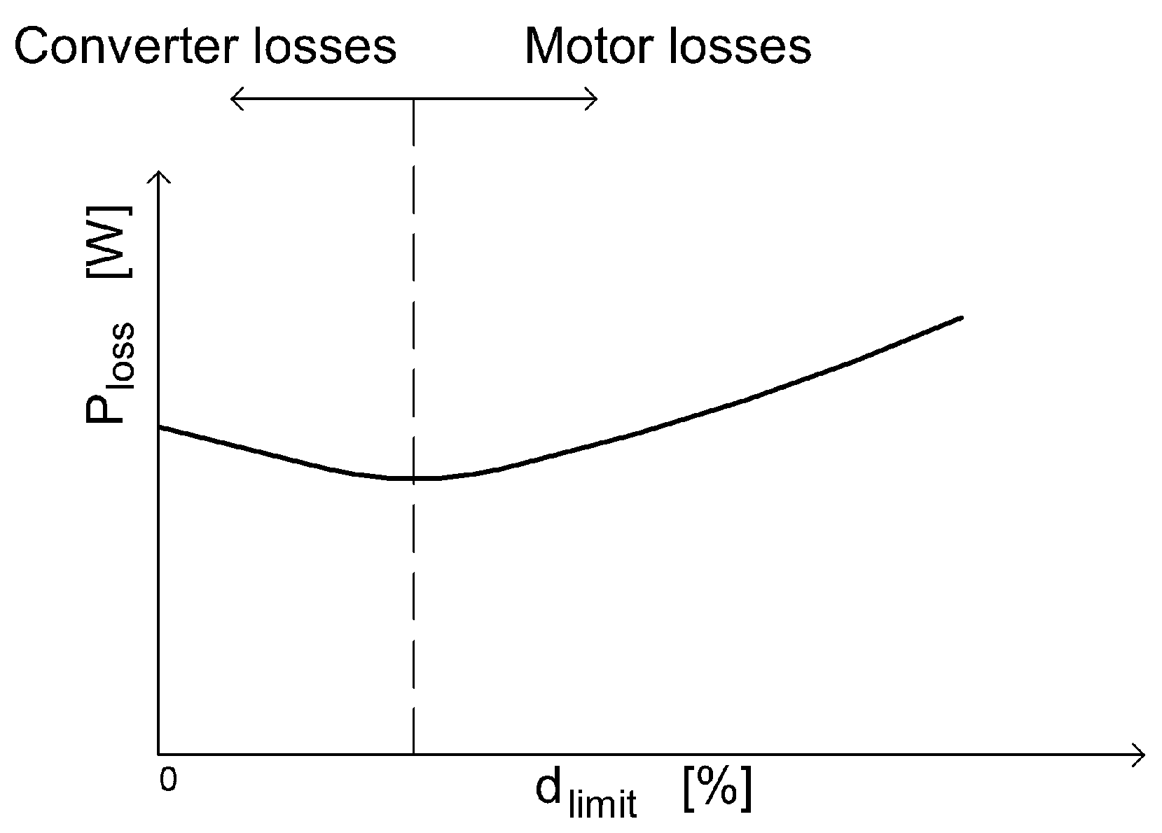
2.2. Drive Losses Analysis
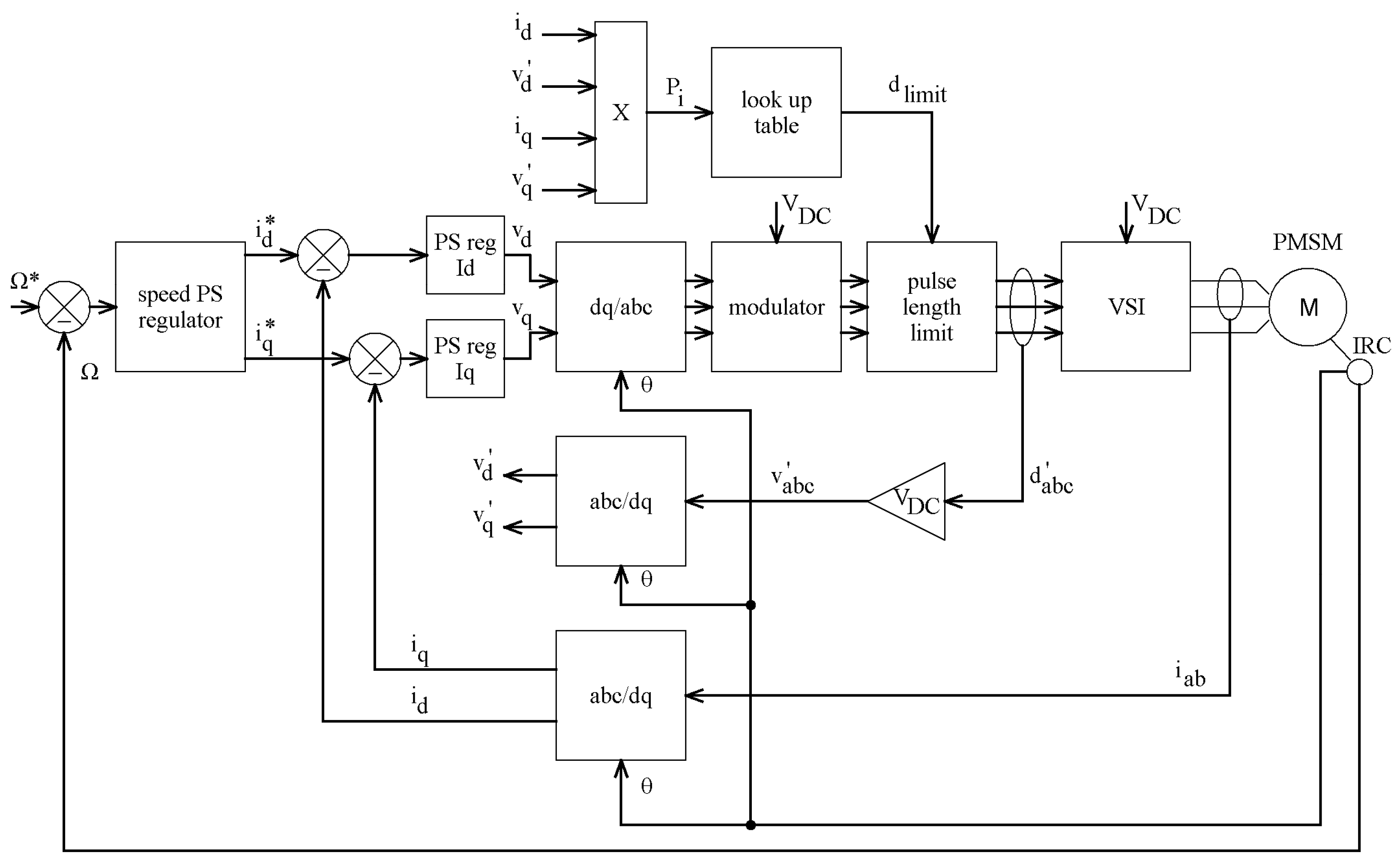
2.3. PMSM Control Strategy
3. Experimental Results
3.1. Experimental Setup
3.2. Pulse Length Limiting
3.3. Current-Collapse Losses Minimization
4. Discussion
Author Contributions
Funding
Conflicts of Interest
References
- Deboy, G.; Treu, M.; Haeberlen, O.; Neumayr, D. Si, SiC and GaN power devices: An unbiased view on key performance indicators. In Proceedings of the 2016 IEEE International Electron Devices Meeting (IEDM), San Francisco, CA, USA, 3–7 December 2016. [Google Scholar]
- Shirabe, K.; Swamy, M.M.; Kang, J.; Hisatsune, M.; Wu, Y.; Kebort, D.; Honea, J. Efficiency Comparison Between Si-IGBT-Based Drive and GaN-Based Drive. IEEE Trans. Ind. Appl. 2014, 50, 566–572. [Google Scholar] [CrossRef]
- Ding, X.; Zhou, Y.; Cheng, J. A review of gallium nitride power device and its applications in motor drive. CES Trans. Electr. Mach. Syst. 2019, 3, 54–64. [Google Scholar] [CrossRef]
- Cai, Y.; Forsyth, A.J.; Todd, R. Impact of GaN HEMT dynamic on-state resistance on converter performance. In Proceedings of the 2017 IEEE Applied Power Electronics Conference and Exposition (APEC), Tampa, FL, USA, 26–30 March 2017. [Google Scholar]
- Joh, J.; Alamo, J.A.; Jimenez, J. A Simple Current Collapse Measurement Technique for GaN High-Electron Mobility Transistors. IEEE Electron Device Lett. 2008, 29, 665–667. [Google Scholar] [CrossRef]
- Vetury, R.; Zhang, N.Q.; Keller, S.; Mishra, U.K. The impact of surface states on the DC and RF characteristics of AlGaN/GaN HFETs. IEEE Trans. Electr. Devices 2001, 48, 560–566. [Google Scholar] [CrossRef]
- Li, R.; Wu, X.; Xie, G.; Sheng, K. Dynamic on-state resistance evaluation of GaN devices under hard and soft switching conditions. In Proceedings of the 2018 IEEE Applied Power Electronics Conference and Exposition (APEC), San Antonio, TX, USA, 4–8 March 2018. [Google Scholar]
- Li, K.; Videt, A.; Idir, N.; Evans, P.; Johnson, M. Experimental Investigation of GaN Transistor Current Collapse on Power Converter Efficiency for Electrical Vehicles. In Proceedings of the 2019 IEEE Vehicle Power and Propulsion Conference (VPPC), Hanoi, Vietnam, 14–17 October 2019. [Google Scholar]
- Do Van Thang, T.; Trovao, J.P.F.; Li, K.; Boulon, L. Wide-Bandgap Power Semiconductors for Electric Vehicle Systems: Challenges and Trends. IEEE Veh. Technol. Mag. 2021, 16, 89–98. [Google Scholar] [CrossRef]
- Koudymov, A.; Shur, M.S.; Simin, G. Compact Model of Current Collapse in Heterostructure Field-Effect Transistors. IEEE Electron Device Lett. 2007, 28, 332–335. [Google Scholar] [CrossRef]
- Zagni, N.; Chini, A.; Puglisi, F.M.; Pavan, P.; Verzellesi, G. On the Modeling of the Donor/Acceptor Compensation Ratio in Carbon-Doped GaN to Univocally Reproduce Breakdown Voltage and Current Collapse in Lateral GaN Power HEMTs. Micromachines 2021, 12, 709. [Google Scholar] [CrossRef] [PubMed]
- Videt, A.; Li, K.; Idir, N.; Evans, P.; Johnson, M. Analysis of GaN Converter Circuit Stability Influenced by Current Collapse Effect. In Proceedings of the 2020 IEEE Applied Power Electronics Conference and Exposition (APEC), New Orleans, LA, USA, 15–19 March 2020. [Google Scholar]
- Tzou, A.-J.; Hsieh, D.-H.; Chen, S.-H.; Liao, Y.-K.; Li, Z.-Y.; Chang, C.-Y.; Kuo, H.-C. An Investigation of Carbon-Doping-Induced Current Collapse in GaN-on-Si High Electron Mobility Transistors. Electronics 2016, 5, 28. [Google Scholar] [CrossRef] [Green Version]
- Li, X.; Posthuma, N.; Bakeroot, B.; Liang, H.; You, S.; Wu, Z.; Zhao, M.; Groeseneken, G.; Decoutere, S. Investigating the Current Collapse Mechanisms of p-GaN Gate HEMTs by Different Passivation Dielectrics. IEEE Trans. Power Electron. 2021, 36, 4927–4930. [Google Scholar] [CrossRef]
- Tanaka, K.; Morita, T.; Umeda, H.; Tamura, S.; Ishida, H.; Ishida, M.; Ueda, T. Mechanism of Current-Collapse-Free Operation in E-Mode GaN Gate Injection Transistors Employed for Efficient Power Conversion. In Proceedings of the 2016 IEEE Compound Semiconductor Integrated Circuit Symposium (CSICS), Austin, TX, USA, 23–26 October 2016. [Google Scholar]
- Yang, J.X.; Lin, D.J.; Wu, Y.R.; Huang, J.J. Deep Source Metal Trenches in GaN-On-Si HEMTs for Relieving Current Collapse. IEEE J. Electron Devices Soc. 2021, 9, 557–563. [Google Scholar] [CrossRef]
- Lin, W.; Wang, M.; Sun, H.; Xie, B.; Wen, C.P.; Hao, Y.; Shen, B. Suppressing Buffer-Induced Current Collapse in GaN HEMTs with a Source-Connected p-GaN (SCPG): A Simulation Study. Electronics 2021, 10, 942. [Google Scholar] [CrossRef]
- Martínez, P.J.; Maset, E.; Martín-Holgado, P.; Morilla, Y.; Gilabert, D.; Sanchis-Kilders, E. Impact of Gamma Radiation on Dynamic RDSON Characteristics in AlGaN/GaN Power HEMTs. Materials 2019, 12, 2760. [Google Scholar] [CrossRef] [PubMed] [Green Version]
- Joh, J.; Tipirneni, N.; Pendharkar, S.; Krishnan, S. Current collapse in GaN heterojunction field effect transistors for high-voltage switching applications. In Proceedings of the 2014 IEEE International Reliability Physics Symposium, Waikoloa, HI, USA, 1–5 June 2014. [Google Scholar]
- Pereira, T.; Liserre, M.; Krischan, K.; Muetze, A. Minimizing Losses Induced by Parasitic Winding Capacitance in Electric Drives by Means of Soft-Switching GaN-Based ARCP. In Proceedings of the 2020 IEEE Energy Conversion Congress and Exposition (ECCE), Detroit, MI, USA, 11–15 October 2020. [Google Scholar]
- Skarolek, P.; Frolov, F.; Lettl, J. GaN Based Inverter Current-Collapse Behavior with Switching Frequency and Blocking Voltage. In Proceedings of the 2021 International Conference on Applied Electronics (AE), Pilsen, Czech Republic, 7–8 September 2021. [Google Scholar]
- Karlovsky, P.; Lipcak, O.; Bauer, J. Iron Loss Minimization Strategy for Predictive Torque Control of Induction Motor. Electronics 2020, 9, 566. [Google Scholar] [CrossRef] [Green Version]
- Ohta, K. Variable Switching Frequency Control for Efficiency Improvement of Motor Drive System by Using GaN Three Phase Inverter. In Proceedings of the 2020 IEEE International Conference on Industrial Technology (ICIT), Buenos Aires, Argentina, 26–28 February 2020. [Google Scholar]
- Yu, G.; Zhang, Y.; Li, Y. Research of DSP-Based SVPWM Vector Control System of Asynchronous Motor. In Proceedings of the 2012 International Conference on Computer Science and Electronics Engineering, Hangzhou, China, 23–25 March 2012. [Google Scholar]
- Yang, G.; Zhang, S.; Zhang, C. Analysis of Core Loss of Permanent Magnet Synchronous Machine for Vehicle Applications under Different Operating Conditions. Appl. Sci. 2020, 10, 7232. [Google Scholar] [CrossRef]
- Zhou, K.; Ai, M.; Sun, D.; Jin, N.; Wu, X. Field Weakening Operation Control Strategies of PMSM Based on Feedback Linearization. Energies 2019, 12, 4526. [Google Scholar] [CrossRef] [Green Version]


| Motor/Generator | |
|---|---|
| Type | USAREM-05CFJ11 |
| RPM | 3000 |
| Power [W] | 500 |
| Max voltage [V] | 200 |
| Max current [A] | 3.6 |
| Stator resistance [Ω] | 1.63 |
| -axis inductance [mH] | 10.3 |
| -axis inductance [mH] | 10.9 |
| Speed | Load | DC-Link Current [A] | Loss Decreased | |
|---|---|---|---|---|
| RPM | Ω | Limit = 0 | Look Up Table | % |
| 1500 | 200 | 0.4020 | 0.3990 | 0.75 |
| 100 | 0.5051 | 0.5030 | 0.42 | |
| 50 | 0.7162 | 0.7120 | 0.59 | |
| 33 | 0.9225 | 0.9170 | 0.60 | |
| 2000 | 200 | 0.5730 | 0.5570 | 2.87 |
| 100 | 0.7470 | 0.7280 | 2.61 | |
| 50 | 1.095 | 1.072 | 2.15 | |
| 33 | 1.446 | 1.418 | 1.97 | |
| 25 | 1.771 | 1.738 | 1.90 | |
Publisher’s Note: MDPI stays neutral with regard to jurisdictional claims in published maps and institutional affiliations. |
© 2022 by the authors. Licensee MDPI, Basel, Switzerland. This article is an open access article distributed under the terms and conditions of the Creative Commons Attribution (CC BY) license (https://creativecommons.org/licenses/by/4.0/).
Share and Cite
Skarolek, P.; Lipcak, O.; Lettl, J. Current Collapse Conduction Losses Minimization in GaN Based PMSM Drive. Electronics 2022, 11, 1503. https://doi.org/10.3390/electronics11091503
Skarolek P, Lipcak O, Lettl J. Current Collapse Conduction Losses Minimization in GaN Based PMSM Drive. Electronics. 2022; 11(9):1503. https://doi.org/10.3390/electronics11091503
Chicago/Turabian StyleSkarolek, Pavel, Ondrej Lipcak, and Jiri Lettl. 2022. "Current Collapse Conduction Losses Minimization in GaN Based PMSM Drive" Electronics 11, no. 9: 1503. https://doi.org/10.3390/electronics11091503